EP0801321A2 - Räumlicher Lichtmodulator und Projektor - Google Patents
Räumlicher Lichtmodulator und Projektor Download PDFInfo
- Publication number
- EP0801321A2 EP0801321A2 EP97302442A EP97302442A EP0801321A2 EP 0801321 A2 EP0801321 A2 EP 0801321A2 EP 97302442 A EP97302442 A EP 97302442A EP 97302442 A EP97302442 A EP 97302442A EP 0801321 A2 EP0801321 A2 EP 0801321A2
- Authority
- EP
- European Patent Office
- Prior art keywords
- electrode
- light
- slm
- layer
- voltage
- Prior art date
- Legal status (The legal status is an assumption and is not a legal conclusion. Google has not performed a legal analysis and makes no representation as to the accuracy of the status listed.)
- Granted
Links
Images



Classifications
-
- G—PHYSICS
- G02—OPTICS
- G02F—OPTICAL DEVICES OR ARRANGEMENTS FOR THE CONTROL OF LIGHT BY MODIFICATION OF THE OPTICAL PROPERTIES OF THE MEDIA OF THE ELEMENTS INVOLVED THEREIN; NON-LINEAR OPTICS; FREQUENCY-CHANGING OF LIGHT; OPTICAL LOGIC ELEMENTS; OPTICAL ANALOGUE/DIGITAL CONVERTERS
- G02F1/00—Devices or arrangements for the control of the intensity, colour, phase, polarisation or direction of light arriving from an independent light source, e.g. switching, gating or modulating; Non-linear optics
- G02F1/01—Devices or arrangements for the control of the intensity, colour, phase, polarisation or direction of light arriving from an independent light source, e.g. switching, gating or modulating; Non-linear optics for the control of the intensity, phase, polarisation or colour
- G02F1/13—Devices or arrangements for the control of the intensity, colour, phase, polarisation or direction of light arriving from an independent light source, e.g. switching, gating or modulating; Non-linear optics for the control of the intensity, phase, polarisation or colour based on liquid crystals, e.g. single liquid crystal display cells
- G02F1/133—Constructional arrangements; Operation of liquid crystal cells; Circuit arrangements
- G02F1/1333—Constructional arrangements; Manufacturing methods
- G02F1/1335—Structural association of cells with optical devices, e.g. polarisers or reflectors
- G02F1/133509—Filters, e.g. light shielding masks
- G02F1/133512—Light shielding layers, e.g. black matrix
-
- G—PHYSICS
- G02—OPTICS
- G02F—OPTICAL DEVICES OR ARRANGEMENTS FOR THE CONTROL OF LIGHT BY MODIFICATION OF THE OPTICAL PROPERTIES OF THE MEDIA OF THE ELEMENTS INVOLVED THEREIN; NON-LINEAR OPTICS; FREQUENCY-CHANGING OF LIGHT; OPTICAL LOGIC ELEMENTS; OPTICAL ANALOGUE/DIGITAL CONVERTERS
- G02F1/00—Devices or arrangements for the control of the intensity, colour, phase, polarisation or direction of light arriving from an independent light source, e.g. switching, gating or modulating; Non-linear optics
- G02F1/01—Devices or arrangements for the control of the intensity, colour, phase, polarisation or direction of light arriving from an independent light source, e.g. switching, gating or modulating; Non-linear optics for the control of the intensity, phase, polarisation or colour
- G02F1/13—Devices or arrangements for the control of the intensity, colour, phase, polarisation or direction of light arriving from an independent light source, e.g. switching, gating or modulating; Non-linear optics for the control of the intensity, phase, polarisation or colour based on liquid crystals, e.g. single liquid crystal display cells
- G02F1/133—Constructional arrangements; Operation of liquid crystal cells; Circuit arrangements
- G02F1/1333—Constructional arrangements; Manufacturing methods
- G02F1/1335—Structural association of cells with optical devices, e.g. polarisers or reflectors
-
- G—PHYSICS
- G02—OPTICS
- G02F—OPTICAL DEVICES OR ARRANGEMENTS FOR THE CONTROL OF LIGHT BY MODIFICATION OF THE OPTICAL PROPERTIES OF THE MEDIA OF THE ELEMENTS INVOLVED THEREIN; NON-LINEAR OPTICS; FREQUENCY-CHANGING OF LIGHT; OPTICAL LOGIC ELEMENTS; OPTICAL ANALOGUE/DIGITAL CONVERTERS
- G02F1/00—Devices or arrangements for the control of the intensity, colour, phase, polarisation or direction of light arriving from an independent light source, e.g. switching, gating or modulating; Non-linear optics
- G02F1/01—Devices or arrangements for the control of the intensity, colour, phase, polarisation or direction of light arriving from an independent light source, e.g. switching, gating or modulating; Non-linear optics for the control of the intensity, phase, polarisation or colour
- G02F1/13—Devices or arrangements for the control of the intensity, colour, phase, polarisation or direction of light arriving from an independent light source, e.g. switching, gating or modulating; Non-linear optics for the control of the intensity, phase, polarisation or colour based on liquid crystals, e.g. single liquid crystal display cells
- G02F1/133—Constructional arrangements; Operation of liquid crystal cells; Circuit arrangements
- G02F1/1333—Constructional arrangements; Manufacturing methods
- G02F1/1343—Electrodes
-
- G—PHYSICS
- G02—OPTICS
- G02F—OPTICAL DEVICES OR ARRANGEMENTS FOR THE CONTROL OF LIGHT BY MODIFICATION OF THE OPTICAL PROPERTIES OF THE MEDIA OF THE ELEMENTS INVOLVED THEREIN; NON-LINEAR OPTICS; FREQUENCY-CHANGING OF LIGHT; OPTICAL LOGIC ELEMENTS; OPTICAL ANALOGUE/DIGITAL CONVERTERS
- G02F1/00—Devices or arrangements for the control of the intensity, colour, phase, polarisation or direction of light arriving from an independent light source, e.g. switching, gating or modulating; Non-linear optics
- G02F1/01—Devices or arrangements for the control of the intensity, colour, phase, polarisation or direction of light arriving from an independent light source, e.g. switching, gating or modulating; Non-linear optics for the control of the intensity, phase, polarisation or colour
- G02F1/13—Devices or arrangements for the control of the intensity, colour, phase, polarisation or direction of light arriving from an independent light source, e.g. switching, gating or modulating; Non-linear optics for the control of the intensity, phase, polarisation or colour based on liquid crystals, e.g. single liquid crystal display cells
- G02F1/133—Constructional arrangements; Operation of liquid crystal cells; Circuit arrangements
- G02F1/135—Liquid crystal cells structurally associated with a photoconducting or a ferro-electric layer, the properties of which can be optically or electrically varied
-
- G—PHYSICS
- G02—OPTICS
- G02F—OPTICAL DEVICES OR ARRANGEMENTS FOR THE CONTROL OF LIGHT BY MODIFICATION OF THE OPTICAL PROPERTIES OF THE MEDIA OF THE ELEMENTS INVOLVED THEREIN; NON-LINEAR OPTICS; FREQUENCY-CHANGING OF LIGHT; OPTICAL LOGIC ELEMENTS; OPTICAL ANALOGUE/DIGITAL CONVERTERS
- G02F1/00—Devices or arrangements for the control of the intensity, colour, phase, polarisation or direction of light arriving from an independent light source, e.g. switching, gating or modulating; Non-linear optics
- G02F1/01—Devices or arrangements for the control of the intensity, colour, phase, polarisation or direction of light arriving from an independent light source, e.g. switching, gating or modulating; Non-linear optics for the control of the intensity, phase, polarisation or colour
- G02F1/13—Devices or arrangements for the control of the intensity, colour, phase, polarisation or direction of light arriving from an independent light source, e.g. switching, gating or modulating; Non-linear optics for the control of the intensity, phase, polarisation or colour based on liquid crystals, e.g. single liquid crystal display cells
- G02F1/133—Constructional arrangements; Operation of liquid crystal cells; Circuit arrangements
- G02F1/135—Liquid crystal cells structurally associated with a photoconducting or a ferro-electric layer, the properties of which can be optically or electrically varied
- G02F1/1351—Light-absorbing or blocking layers
-
- G—PHYSICS
- G02—OPTICS
- G02F—OPTICAL DEVICES OR ARRANGEMENTS FOR THE CONTROL OF LIGHT BY MODIFICATION OF THE OPTICAL PROPERTIES OF THE MEDIA OF THE ELEMENTS INVOLVED THEREIN; NON-LINEAR OPTICS; FREQUENCY-CHANGING OF LIGHT; OPTICAL LOGIC ELEMENTS; OPTICAL ANALOGUE/DIGITAL CONVERTERS
- G02F1/00—Devices or arrangements for the control of the intensity, colour, phase, polarisation or direction of light arriving from an independent light source, e.g. switching, gating or modulating; Non-linear optics
- G02F1/01—Devices or arrangements for the control of the intensity, colour, phase, polarisation or direction of light arriving from an independent light source, e.g. switching, gating or modulating; Non-linear optics for the control of the intensity, phase, polarisation or colour
- G02F1/13—Devices or arrangements for the control of the intensity, colour, phase, polarisation or direction of light arriving from an independent light source, e.g. switching, gating or modulating; Non-linear optics for the control of the intensity, phase, polarisation or colour based on liquid crystals, e.g. single liquid crystal display cells
- G02F1/133—Constructional arrangements; Operation of liquid crystal cells; Circuit arrangements
- G02F1/135—Liquid crystal cells structurally associated with a photoconducting or a ferro-electric layer, the properties of which can be optically or electrically varied
- G02F1/1352—Light-reflecting layers
-
- G—PHYSICS
- G02—OPTICS
- G02F—OPTICAL DEVICES OR ARRANGEMENTS FOR THE CONTROL OF LIGHT BY MODIFICATION OF THE OPTICAL PROPERTIES OF THE MEDIA OF THE ELEMENTS INVOLVED THEREIN; NON-LINEAR OPTICS; FREQUENCY-CHANGING OF LIGHT; OPTICAL LOGIC ELEMENTS; OPTICAL ANALOGUE/DIGITAL CONVERTERS
- G02F2203/00—Function characteristic
- G02F2203/02—Function characteristic reflective
Definitions
- FIG. 9 is a perspective view of part of a conventional spatial light modulator (SLM).
- a transparent electrode 92b is formed on a glass substrate 91b, and an amorphous silicon (a-Si) photoconductor layer 93 etched in a grid pattern is formed on the transparent electrode 92b.
- the grid-shaped grooves formed by etching are filled with a light-blocking material.
- a reflective electrode 95 comprising plural divided electrodes is formed in the rectangular parts defined by and between the grooves of this grid.
- Another transparent electrode 92a is formed on a further glass substrate 91a.
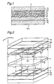
- the next step is to remove the layer with the lowest resistance, i.e., the n layer, from the a-Si photoconductor layer 3 by means of active ion etching using the gap pattern of the drive electrode 8 (FIG. 3C). Any two adjacent electrodes in the drive electrode 8 can thus be electrically isolated.
- a 1000 ⁇ thick aluminum layer is then formed by sputtering onto the same surface of the light blocking layer 4 in which the contact holes 9 were formed (FIG. 3F).
- This aluminum layer is then segmented by a photolithographic method to form the reflective electrode 5.
- this reflective electrode 5 comprises plural square electrodes formed at a 40 ⁇ m pitch with a 5 ⁇ m gap between adjacent electrodes.
- Each of the electrodes in the reflective electrode 5 is also passed through a contact hole 9 in the light blocking layer 4 and electrically connected to the corresponding electrode of the drive electrode 8.
- rubbing rollers are used for an alignment treat.
- Each electrode in the drive electrode 8 applies the voltage generated by the a-Si photoconductor layer 3 to the corresponding electrode of the reflective electrode 5 through the contact hole 9 in the light blocking layer 4.
- each electrode in the reflective electrode 5 applies to the LC layer 6 a voltage corresponding to the brightness of each pixel in the input image projected onto the a-Si photoconductor layer 3.
- the SLM 100 modulates and reflects the strong incident light from the glass substrate la side of the SLM 100 according to the brightness of each pixel in the input image projected from the glass substrate 1b side of the SLM 100 onto the a-Si photoconductor layer 3.
- the light blocking layer 4 is provided to prevent misoperation of the a-Si photoconductor layer 3 due to leakage of strong incident light from the glass substrate la side to the a-Si photoconductor layer 3.
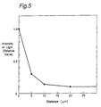
- FIG. 5 is a graph of the relationship between the intensity of leakage light and the gap pattern offset when the reflective electrode 5 is moved parallel to the drive electrode 8 in the direction of the arrow shown in FIG. 4.
- the intensity of light leaking to the a-Si photoconductor layer 3 when the gap overlap area is greatest-, i.e., when the gap patterns are coincident, is 1.
- the intensity of the leaked light is 13% when the reflective electrode 5 is moved 10 ⁇ m, i.e., approximately 7 ⁇ m in both x- and y-axis directions, and there is negligible further reduction achieved relative to any greater distance moved.
- the electrodes of the reflective electrode 5 and drive electrode 8 have been described by way of example only above as square in shape, the invention shall not be so limited and said electrodes can be otherwise polygonally shaped with the same effects achieved. For example, the same effects can be achieved when the electrodes are hexagonally shaped.
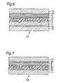
- a spatial light modulator according to the second embodiment of the present invention is described below with reference to FIG. 7, a cross section of part of a spatial light modulator (SLM) 102 according to said second embodiment. Note that parts of like function are referenced using the same reference numbers in FIG. 7 as in FIG. 1 and FIG. 2, and further description thereof is thus omitted below.
- SLM spatial light modulator
- a voltage storage circuit comprising the silicon substrate 11 and active element 31 and applying a voltage according to the input image to the electrodes of the drive electrode 8 is used as the voltage applying means in this embodiment. Note that this voltage applying means writes electrically using an electrical signal, and thus differs from the optical-writing method of the first embodiment.
- a voltage corresponding to the brightness of each pixel in the input image is applied from an external source to the active element 31 as an electrical signal, and is accumulated in each TFT.
- Each electrode of the drive electrode 81 applies the voltage stored by each TFT of the active element 31 to the corresponding electrode of the reflective electrode 5 via a contact hole 91 in the light blocking layer 41.
- each electrode in the reflective electrode 5 applies to the LC layer 6 a voltage corresponding to the brightness of the corresponding pixel in the input image.
- the SLM 102 modulates and reflects the strong incident light from the glass substrate la side of the SLM 102 according to the brightness of each pixel in the input image.
- the light blocking layer 41 is provided below the reflective electrode 5 covering the TFT on the glass substrate to prevent misoperation of the TFT due to leakage of strong incident light from the glass substrate la side.
- the same effect can be achieved by using a MOS transistor on a silicon substrate in place of a TFT as the active element, or using random access memory (RAM) on a silicon substrate as the voltage storage circuit.
- a MOS transistor on a silicon substrate in place of a TFT as the active element
- RAM random access memory
- FIG. 8 is a block diagram of a projector applying the SLM 100 of the present invention.
- the projector of the invention comprises an SLM 100, a CRT 50, a write lens 51, a light source 52, a polarized beam splitter 53, a projection lens 54, a screen 55, and a pre-polarizer 56.
- the image displayed on the CRT 50 is condensed by the write lens 51 and projected through the glass substrate 1b and transparent electrode 2b of the SLM 100 onto the a-Si photoconductor layer 3.
- the light source 52 emits a strong beam to the pre-polirizer 56.
- the pre-polirizer 56 separates the light from the light source 52 into p and s waves, and passes only the p wave component.
- the polarized beam splitter 53 reflects only the p wave component of the emitted beam and passes the s wave component.
- This p wave component incident light is then modulated to s wave light by the LC layer 6 according to the voltage applied by the reflective electrode 5, and is then reflected by the reflective electrode 5.
- the reflected light reflected by the SLM 100 contains an s wave component corresponding to the brightness of each pixel in the input image from the CRT 50.
- the s wave component of this light produced by the SLM 100 passes the polarized beam splitter 53, is condensed by the projection lens 54, and projected onto the screen 55.
- the electrical-write type SLM 102 described above as the second embodiment can be used in place of the optical-write type SLM 100 above. It is also possible to provide an image signal source outputting an electrical signal as the input image in place of the CRT 50 and write lens 51 used above with the output signal of this image signal source input to the SLM 102.
Landscapes
- Physics & Mathematics (AREA)
- Nonlinear Science (AREA)
- Mathematical Physics (AREA)
- Chemical & Material Sciences (AREA)
- Crystallography & Structural Chemistry (AREA)
- General Physics & Mathematics (AREA)
- Optics & Photonics (AREA)
- Liquid Crystal (AREA)
- Projection Apparatus (AREA)
Applications Claiming Priority (3)
| Application Number | Priority Date | Filing Date | Title |
|---|---|---|---|
| JP8922396 | 1996-04-11 | ||
| JP89223/96 | 1996-04-11 | ||
| JP8922396 | 1996-04-11 |
Publications (3)
| Publication Number | Publication Date |
|---|---|
| EP0801321A2 true EP0801321A2 (de) | 1997-10-15 |
| EP0801321A3 EP0801321A3 (de) | 1998-07-01 |
| EP0801321B1 EP0801321B1 (de) | 2002-08-21 |
Family
ID=13964740
Family Applications (1)
| Application Number | Title | Priority Date | Filing Date |
|---|---|---|---|
| EP97302442A Expired - Lifetime EP0801321B1 (de) | 1996-04-11 | 1997-04-09 | Räumlicher Lichtmodulator und Projektor |
Country Status (4)
| Country | Link |
|---|---|
| US (1) | US5798806A (de) |
| EP (1) | EP0801321B1 (de) |
| KR (1) | KR100228886B1 (de) |
| DE (1) | DE69714807T2 (de) |
Families Citing this family (9)
| Publication number | Priority date | Publication date | Assignee | Title |
|---|---|---|---|---|
| JPH1184409A (ja) * | 1997-09-01 | 1999-03-26 | Canon Inc | 静止画像表示装置 |
| JP4245292B2 (ja) * | 2001-12-06 | 2009-03-25 | シャープ株式会社 | トランジスタアレイ、アクティブマトリクス基板、表示装置、並びにトランジスタアレイおよびアクティブマトリクス基板の製造方法 |
| KR100978949B1 (ko) * | 2003-12-05 | 2010-08-31 | 엘지디스플레이 주식회사 | 반투과형 액정표시장치 |
| JP2006049308A (ja) * | 2004-08-04 | 2006-02-16 | Samsung Electronics Co Ltd | 表示装置、その製造方法、及びその製造装置 |
| CN101501748B (zh) * | 2006-04-19 | 2012-12-05 | 伊格尼斯创新有限公司 | 有源矩阵显示器的稳定驱动设计 |
| KR101607636B1 (ko) * | 2009-11-23 | 2016-04-12 | 삼성디스플레이 주식회사 | 액정 표시 장치 |
| USD896994S1 (en) * | 2017-10-03 | 2020-09-22 | Alexander Lorenz | Concrete slab |
| USD962484S1 (en) * | 2017-10-03 | 2022-08-30 | Alexander Lorenz | Concrete slab |
| WO2020150523A1 (en) * | 2019-01-18 | 2020-07-23 | Dolby Laboratories Licensing Corporation | Attenuating wavefront determination for noise reduction |
Family Cites Families (16)
| Publication number | Priority date | Publication date | Assignee | Title |
|---|---|---|---|---|
| US4239346A (en) * | 1979-05-23 | 1980-12-16 | Hughes Aircraft Company | Compact liquid crystal display system |
| US4913531A (en) * | 1988-09-07 | 1990-04-03 | Hughes Aircraft Company | Liquid crystal light valve with grooved microgrid and method of forming the same |
| JP3176661B2 (ja) * | 1991-10-03 | 2001-06-18 | セイコーインスツルメンツ株式会社 | 光書込型空間光変調器、およびその感度調整方法 |
| US5384649A (en) * | 1991-12-26 | 1995-01-24 | Matsushita Electric Industrial Co., Ltd. | Liquid crystal spatial light modulator with electrically isolated reflecting films connected to electrically isolated pixel portions of photo conductor |
| JPH05333366A (ja) * | 1992-05-28 | 1993-12-17 | Matsushita Electric Ind Co Ltd | 空間光変調素子 |
| US5416621A (en) * | 1992-06-11 | 1995-05-16 | Matsushita Electric Industrial Co., Ltd. | Driving method for ferroelectric liquid crystal spatial light modulator |
| JPH0643482A (ja) * | 1992-07-24 | 1994-02-18 | Matsushita Electric Ind Co Ltd | 空間光変調素子およびその製造方法 |
| JPH0651341A (ja) * | 1992-07-31 | 1994-02-25 | Nippon Hoso Kyokai <Nhk> | 空間光変調素子 |
| JP2848741B2 (ja) * | 1992-08-11 | 1999-01-20 | シャープ株式会社 | 液晶空間光変調素子 |
| US5461501A (en) * | 1992-10-08 | 1995-10-24 | Hitachi, Ltd. | Liquid crystal substrate having 3 metal layers with slits offset to block light from reaching the substrate |
| JPH06347819A (ja) * | 1993-06-08 | 1994-12-22 | Matsushita Electric Ind Co Ltd | 空間光変調素子 |
| JPH06347820A (ja) * | 1993-06-08 | 1994-12-22 | Matsushita Electric Ind Co Ltd | 空間光変調素子の製造方法 |
| EP0642050B1 (de) * | 1993-09-02 | 2002-01-30 | Matsushita Electric Industrial Co., Ltd. | Räumlicher Lichtmodulator, Herstellungsverfahren und Anzeigevorrichtung vom Projektionstyp |
| US5612798A (en) * | 1994-05-31 | 1997-03-18 | Tuli; Raja S. | Optically addressed liquid crystal display device having a matrix array of photocells |
| JP3062012B2 (ja) * | 1994-08-25 | 2000-07-10 | シャープ株式会社 | 液晶ライトバルブ |
| US5612800A (en) * | 1994-11-02 | 1997-03-18 | Hughes Aircraft Company | LCLV having photoconductive pedestals each having a cross-sectional area no greater than 5 percent of the area of its respective reflective pad |
-
1997
- 1997-04-09 DE DE69714807T patent/DE69714807T2/de not_active Expired - Fee Related
- 1997-04-09 EP EP97302442A patent/EP0801321B1/de not_active Expired - Lifetime
- 1997-04-10 US US08/843,611 patent/US5798806A/en not_active Expired - Fee Related
- 1997-04-10 KR KR1019970013306A patent/KR100228886B1/ko not_active Expired - Fee Related
Also Published As
| Publication number | Publication date |
|---|---|
| EP0801321B1 (de) | 2002-08-21 |
| EP0801321A3 (de) | 1998-07-01 |
| DE69714807T2 (de) | 2003-04-24 |
| US5798806A (en) | 1998-08-25 |
| KR970071076A (ko) | 1997-11-07 |
| KR100228886B1 (ko) | 1999-11-01 |
| DE69714807D1 (de) | 2002-09-26 |
Similar Documents
| Publication | Publication Date | Title |
|---|---|---|
| JP3824290B2 (ja) | アレイ型光変調素子、アレイ型露光素子、及び平面型ディスプレイ、並びにアレイ型光変調素子の駆動方法 | |
| KR100402506B1 (ko) | 전기 광학 장치 | |
| JP2694126B2 (ja) | 液晶表示装置及びその製造方法 | |
| US6317187B1 (en) | Liquid crystal light valve apparatus in which the spacers having protrusion and recess | |
| US7133108B2 (en) | Liquid crystal display device | |
| JPH02131221A (ja) | 光導電型液昌ライトバルブ | |
| US5798806A (en) | Spatial light modulator and projector | |
| JP4085369B2 (ja) | 液晶表示装置 | |
| JPH11109360A (ja) | 液晶表示装置 | |
| US7230666B2 (en) | Liquid crystal display with nonconductive portions in specific areas | |
| JP3334676B2 (ja) | 液晶表示装置 | |
| US7283191B2 (en) | Liquid crystal display device and electronic apparatus wherein liquid crystal molecules having particular pre-tilt angle | |
| JPH0769532B2 (ja) | 投影型表示装置 | |
| WO2023142092A1 (zh) | 液晶手写板及其制造方法 | |
| JPH0833548B2 (ja) | 液晶表示装置 | |
| JPH0212224A (ja) | 液晶表示装置 | |
| JP3048705B2 (ja) | 液晶表示装置 | |
| JPH09113928A (ja) | 投影型画像表示装置 | |
| EP0515150A2 (de) | Lichtadressierte Flüssigkristallanzeigevorrichtung | |
| CN102445789A (zh) | 液晶装置、液晶装置的制造方法以及电子设备 | |
| KR100931588B1 (ko) | 액정표시장치 및 이의 제조 방법 | |
| JPH1031226A (ja) | 空間光変調素子と投写装置 | |
| JP2022055778A (ja) | 電気光学装置および電子機器 | |
| US7420633B2 (en) | Liquid crystal display having particular irregularity controlling structure | |
| JP2000512037A (ja) | 目に見えない継ぎ目を備えた平坦なタイルパネルディスプレイ |
Legal Events
| Date | Code | Title | Description |
|---|---|---|---|
| PUAI | Public reference made under article 153(3) epc to a published international application that has entered the european phase |
Free format text: ORIGINAL CODE: 0009012 |
|
| 17P | Request for examination filed |
Effective date: 19970502 |
|
| AK | Designated contracting states |
Kind code of ref document: A2 Designated state(s): DE FR GB NL |
|
| PUAL | Search report despatched |
Free format text: ORIGINAL CODE: 0009013 |
|
| AK | Designated contracting states |
Kind code of ref document: A3 Designated state(s): DE FR GB NL |
|
| 17Q | First examination report despatched |
Effective date: 19990716 |
|
| GRAG | Despatch of communication of intention to grant |
Free format text: ORIGINAL CODE: EPIDOS AGRA |
|
| GRAG | Despatch of communication of intention to grant |
Free format text: ORIGINAL CODE: EPIDOS AGRA |
|
| GRAH | Despatch of communication of intention to grant a patent |
Free format text: ORIGINAL CODE: EPIDOS IGRA |
|
| GRAH | Despatch of communication of intention to grant a patent |
Free format text: ORIGINAL CODE: EPIDOS IGRA |
|
| GRAA | (expected) grant |
Free format text: ORIGINAL CODE: 0009210 |
|
| AK | Designated contracting states |
Kind code of ref document: B1 Designated state(s): DE FR GB NL |
|
| REG | Reference to a national code |
Ref country code: GB Ref legal event code: FG4D |
|
| REF | Corresponds to: |
Ref document number: 69714807 Country of ref document: DE Date of ref document: 20020926 |
|
| ET | Fr: translation filed | ||
| PG25 | Lapsed in a contracting state [announced via postgrant information from national office to epo] |
Ref country code: GB Free format text: LAPSE BECAUSE OF NON-PAYMENT OF DUE FEES Effective date: 20030409 |
|
| PLBE | No opposition filed within time limit |
Free format text: ORIGINAL CODE: 0009261 |
|
| STAA | Information on the status of an ep patent application or granted ep patent |
Free format text: STATUS: NO OPPOSITION FILED WITHIN TIME LIMIT |
|
| 26N | No opposition filed |
Effective date: 20030522 |
|
| PG25 | Lapsed in a contracting state [announced via postgrant information from national office to epo] |
Ref country code: DE Free format text: LAPSE BECAUSE OF NON-PAYMENT OF DUE FEES Effective date: 20031101 |
|
| GBPC | Gb: european patent ceased through non-payment of renewal fee |
Effective date: 20030409 |
|
| PG25 | Lapsed in a contracting state [announced via postgrant information from national office to epo] |
Ref country code: FR Free format text: LAPSE BECAUSE OF NON-PAYMENT OF DUE FEES Effective date: 20031231 |
|
| REG | Reference to a national code |
Ref country code: FR Ref legal event code: ST |
|
| PGFP | Annual fee paid to national office [announced via postgrant information from national office to epo] |
Ref country code: NL Payment date: 20060417 Year of fee payment: 10 |
|
| NLV4 | Nl: lapsed or anulled due to non-payment of the annual fee |
Effective date: 20071101 |
|
| PG25 | Lapsed in a contracting state [announced via postgrant information from national office to epo] |
Ref country code: NL Free format text: LAPSE BECAUSE OF NON-PAYMENT OF DUE FEES Effective date: 20071101 |