EP0801415A2 - Magnetrongerät für ganzflächige Niederdruckerosion - Google Patents
Magnetrongerät für ganzflächige Niederdruckerosion Download PDFInfo
- Publication number
- EP0801415A2 EP0801415A2 EP97104017A EP97104017A EP0801415A2 EP 0801415 A2 EP0801415 A2 EP 0801415A2 EP 97104017 A EP97104017 A EP 97104017A EP 97104017 A EP97104017 A EP 97104017A EP 0801415 A2 EP0801415 A2 EP 0801415A2
- Authority
- EP
- European Patent Office
- Prior art keywords
- target
- magnet assembly
- magnetic field
- sputtering
- chamber
- Prior art date
- Legal status (The legal status is an assumption and is not a legal conclusion. Google has not performed a legal analysis and makes no representation as to the accuracy of the status listed.)
- Granted
Links
- 230000003628 erosive effect Effects 0.000 title description 13
- 238000004544 sputter deposition Methods 0.000 claims abstract description 66
- 238000000034 method Methods 0.000 claims abstract description 35
- 239000000463 material Substances 0.000 claims abstract description 15
- 230000007246 mechanism Effects 0.000 claims abstract description 12
- 239000000758 substrate Substances 0.000 claims description 32
- 238000010408 sweeping Methods 0.000 claims description 7
- 230000001965 increasing effect Effects 0.000 claims description 6
- 238000000151 deposition Methods 0.000 description 28
- 230000008021 deposition Effects 0.000 description 27
- 230000008569 process Effects 0.000 description 9
- 238000004140 cleaning Methods 0.000 description 7
- 239000007789 gas Substances 0.000 description 7
- 230000004907 flux Effects 0.000 description 6
- 235000012431 wafers Nutrition 0.000 description 6
- 238000000429 assembly Methods 0.000 description 5
- 230000000712 assembly Effects 0.000 description 5
- 238000011109 contamination Methods 0.000 description 5
- NJPPVKZQTLUDBO-UHFFFAOYSA-N novaluron Chemical compound C1=C(Cl)C(OC(F)(F)C(OC(F)(F)F)F)=CC=C1NC(=O)NC(=O)C1=C(F)C=CC=C1F NJPPVKZQTLUDBO-UHFFFAOYSA-N 0.000 description 4
- 239000002245 particle Substances 0.000 description 4
- XKRFYHLGVUSROY-UHFFFAOYSA-N Argon Chemical group [Ar] XKRFYHLGVUSROY-UHFFFAOYSA-N 0.000 description 3
- 230000008901 benefit Effects 0.000 description 3
- 230000009977 dual effect Effects 0.000 description 3
- 239000000696 magnetic material Substances 0.000 description 3
- 229910000831 Steel Inorganic materials 0.000 description 2
- 238000005137 deposition process Methods 0.000 description 2
- 230000000368 destabilizing effect Effects 0.000 description 2
- 150000002500 ions Chemical class 0.000 description 2
- 238000001465 metallisation Methods 0.000 description 2
- 238000002294 plasma sputter deposition Methods 0.000 description 2
- 239000010959 steel Substances 0.000 description 2
- RTAQQCXQSZGOHL-UHFFFAOYSA-N Titanium Chemical compound [Ti] RTAQQCXQSZGOHL-UHFFFAOYSA-N 0.000 description 1
- NRTOMJZYCJJWKI-UHFFFAOYSA-N Titanium nitride Chemical compound [Ti]#N NRTOMJZYCJJWKI-UHFFFAOYSA-N 0.000 description 1
- 229910052782 aluminium Inorganic materials 0.000 description 1
- XAGFODPZIPBFFR-UHFFFAOYSA-N aluminium Chemical compound [Al] XAGFODPZIPBFFR-UHFFFAOYSA-N 0.000 description 1
- 238000000637 aluminium metallisation Methods 0.000 description 1
- 229910052786 argon Inorganic materials 0.000 description 1
- 230000002238 attenuated effect Effects 0.000 description 1
- 230000004888 barrier function Effects 0.000 description 1
- UTKFUXQDBUMJSX-UHFFFAOYSA-N boron neodymium Chemical compound [B].[Nd] UTKFUXQDBUMJSX-UHFFFAOYSA-N 0.000 description 1
- 239000000919 ceramic Substances 0.000 description 1
- KPLQYGBQNPPQGA-UHFFFAOYSA-N cobalt samarium Chemical compound [Co].[Sm] KPLQYGBQNPPQGA-UHFFFAOYSA-N 0.000 description 1
- 230000001427 coherent effect Effects 0.000 description 1
- 239000002826 coolant Substances 0.000 description 1
- 230000008878 coupling Effects 0.000 description 1
- 238000010168 coupling process Methods 0.000 description 1
- 238000005859 coupling reaction Methods 0.000 description 1
- 230000001419 dependent effect Effects 0.000 description 1
- 238000010586 diagram Methods 0.000 description 1
- 239000012777 electrically insulating material Substances 0.000 description 1
- 238000010893 electron trap Methods 0.000 description 1
- 230000002708 enhancing effect Effects 0.000 description 1
- 238000001755 magnetron sputter deposition Methods 0.000 description 1
- 229910052751 metal Inorganic materials 0.000 description 1
- 239000002184 metal Substances 0.000 description 1
- 230000035699 permeability Effects 0.000 description 1
- 229910000938 samarium–cobalt magnet Inorganic materials 0.000 description 1
- 239000004065 semiconductor Substances 0.000 description 1
- 239000013077 target material Substances 0.000 description 1
- 239000010936 titanium Substances 0.000 description 1
- 229910052719 titanium Inorganic materials 0.000 description 1
- WFKWXMTUELFFGS-UHFFFAOYSA-N tungsten Chemical compound [W] WFKWXMTUELFFGS-UHFFFAOYSA-N 0.000 description 1
- 229910052721 tungsten Inorganic materials 0.000 description 1
- 239000010937 tungsten Substances 0.000 description 1
- XLYOFNOQVPJJNP-UHFFFAOYSA-N water Substances O XLYOFNOQVPJJNP-UHFFFAOYSA-N 0.000 description 1
Images

Classifications
-
- H—ELECTRICITY
- H01—ELECTRIC ELEMENTS
- H01J—ELECTRIC DISCHARGE TUBES OR DISCHARGE LAMPS
- H01J37/00—Discharge tubes with provision for introducing objects or material to be exposed to the discharge, e.g. for the purpose of examination or processing thereof
- H01J37/32—Gas-filled discharge tubes
- H01J37/34—Gas-filled discharge tubes operating with cathodic sputtering
- H01J37/3488—Constructional details of particle beam apparatus not otherwise provided for, e.g. arrangement, mounting, housing, environment; special provisions for cleaning or maintenance of the apparatus
- H01J37/3494—Adaptation to extreme pressure conditions
-
- C—CHEMISTRY; METALLURGY
- C23—COATING METALLIC MATERIAL; COATING MATERIAL WITH METALLIC MATERIAL; CHEMICAL SURFACE TREATMENT; DIFFUSION TREATMENT OF METALLIC MATERIAL; COATING BY VACUUM EVAPORATION, BY SPUTTERING, BY ION IMPLANTATION OR BY CHEMICAL VAPOUR DEPOSITION, IN GENERAL; INHIBITING CORROSION OF METALLIC MATERIAL OR INCRUSTATION IN GENERAL
- C23C—COATING METALLIC MATERIAL; COATING MATERIAL WITH METALLIC MATERIAL; SURFACE TREATMENT OF METALLIC MATERIAL BY DIFFUSION INTO THE SURFACE, BY CHEMICAL CONVERSION OR SUBSTITUTION; COATING BY VACUUM EVAPORATION, BY SPUTTERING, BY ION IMPLANTATION OR BY CHEMICAL VAPOUR DEPOSITION, IN GENERAL
- C23C14/00—Coating by vacuum evaporation, by sputtering or by ion implantation of the coating forming material
- C23C14/22—Coating by vacuum evaporation, by sputtering or by ion implantation of the coating forming material characterised by the process of coating
- C23C14/34—Sputtering
- C23C14/35—Sputtering by application of a magnetic field, e.g. magnetron sputtering
-
- H—ELECTRICITY
- H01—ELECTRIC ELEMENTS
- H01J—ELECTRIC DISCHARGE TUBES OR DISCHARGE LAMPS
- H01J37/00—Discharge tubes with provision for introducing objects or material to be exposed to the discharge, e.g. for the purpose of examination or processing thereof
- H01J37/32—Gas-filled discharge tubes
- H01J37/34—Gas-filled discharge tubes operating with cathodic sputtering
- H01J37/3402—Gas-filled discharge tubes operating with cathodic sputtering using supplementary magnetic fields
- H01J37/3405—Magnetron sputtering
- H01J37/3408—Planar magnetron sputtering
-
- H—ELECTRICITY
- H01—ELECTRIC ELEMENTS
- H01J—ELECTRIC DISCHARGE TUBES OR DISCHARGE LAMPS
- H01J37/00—Discharge tubes with provision for introducing objects or material to be exposed to the discharge, e.g. for the purpose of examination or processing thereof
- H01J37/32—Gas-filled discharge tubes
- H01J37/34—Gas-filled discharge tubes operating with cathodic sputtering
- H01J37/3411—Constructional aspects of the reactor
- H01J37/345—Magnet arrangements in particular for cathodic sputtering apparatus
- H01J37/3455—Movable magnets
Definitions
- the invention relates to magnetrons (e.g. planar magnetrons) such as are used in plasma sputtering systems.
- magnetrons e.g. planar magnetrons
- the magnetron source acts to increase the electron density in the plasma discharge.
- the magnets that are placed behind the target generate magnetic field lines, a portiion of which are somewhat parallel to the face of the target. These magnetic field lines, along with E fields of the electric circuit create forces acting on the electrons which tend to trap them next to the surface of the target. This increases the probability of collisions with the gas (e.g. argon) atoms thereby producing more gas ions to bombard the target.
- the gas e.g. argon
- the magnet assembly is typically moved over the backside of the target so as to produce on average a substantially uniform magnetic field over the entire face of the target from its center to its outer edges. Achieving uniform erosion is particularly desirable for a number of reasons including prolonging target life and producing uniform bottom coverage during deposition of metal into high aspect ratio contact holes. Additionally, uniform sputtering ensures that all regions of the target are continuously eroded, thereby preventing material from back sputtering onto non-active (i.e., non-sputtered) areas and then flaking off.
- Low pressure operation and uniformity in target erosion, particularly at the target's edge are, however, competing objectives.
- low pressure operation is achieved by accepting less uniform target erosion.
- improved uniformity in target erosion typically results in having to operate at higher chamber pressures.
- the invention is a method for controlling the operation of a magnetron source for sputtering a surface of a target in a vacuum chamber.
- the method includes the steps of: (1) during a low pressure phase of sputtering in which the chamber is at a first pressure, causing a magnetic field generated by the magnet assembly to be confined primarily to an inner region of the surface of the target so as to reduce leakage of electrons away from the target during sputtering; and (2) during a subsequent high pressure phase of sputtering in which the chamber is at a second pressure, causing the magnetic field generated by the magnet assembly to extend into an outer region surrounding the inner region so as to sputter material from the outer region of the surface of the target.
- the low pressure phase uses a chamber pressure of less than 1 mTorr and the high pressure phase uses a chamber pressure of greater than 1 mTorr.
- the step of causing the magnetic field to be confined primarily within the inner region of the target's surface involves sweeping the magnet assembly within a first area behind the target, wherein the first area is smaller than the area of the target's surface, and the step of causing the magnetic field to extend into the outer region of the target's surface involves sweeping the magnet assembly into a region that extends beyond the first area.
- the step of causing the magnetic field to extend into the outer region of the target involves causing the magnetic field to spend a larger portion of time in the outer region than it spends in the inner region.
- the low pressure sputtering is performed on a substrate and the method further involves after the low pressure sputtering onto the substrate, inserting a shutter between the substrate and the target; and then performing the high pressure sputtering onto the shutter.
- the second magnet assembly includes a plurality of magnets positioned around a perimeter of the first magnet assembly, and it includes a lift mechanism to which the plurality of magnets are connected. During operation, the lift mechanism raises and lowers the plurality of magnets so as to decrease and increase, respectively, the magnetic field in the outer region.
- the lift mechanism includes one or more actuators to which the plurality of magnets are connected.
- the magnetron source also includes a motor which rotates the first magnet assembly during operation.
- the first magnet assembly includes a shaft by which the first magnet assembly is rotated and output of the motor is coupled to the shaft through a drive belt or direct drive.
- the magnetron source which utilizes a magnet assembly that is smaller than the area of the target, has two modes of operation.
- an initial deposition mode of operation e.g. to coat the bottoms of the contact holes
- low total chamber pressure e.g. ⁇ 1 mTorr
- the magnet assembly is moved so that the magnetic field sweeps over and is confined within an inner region of the target. Since the magnetic field is thereby kept away from the grounded shield and other hardware near the perimeter of the target, stable low pressure operation is possible.
- a subsequent deposition or cleaning mode which is performed at high total chamber pressure (e.g.
- the magnet assembly is moved so that the magnetic field sweeps out to the edge of the target (i.e., into the outer region surrounding the inner region). Since a higher chamber pressure is used, the magnetic field can be brought closer to the edge of the target without destabilizing the plasma. Thus, in the high pressure mode of operation, it becomes possible to sputter the outer region of the target.
- the high pressure mode of operation can be used to create a more uniform thickness of the deposited layer on the substrate or, alternatively, it can be performed as a target cleaning step on a shutter after the substrate has been removed from the chamber.
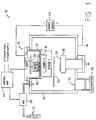
- a sputter deposition system 10 constructed in accordance with the invention includes a vacuum chamber 12 with a dual mode, planar magnetron source 14, a sputter target 16 which is attached to the magnetron source, and a pedestal 18 for holding a substrate 20 (e.g. semiconductor wafer) onto which material that is sputtered from target 16 is to be deposited.
- the area of magnet assembly 22 (e.g. the area of the projection of the magnets onto the surface of the target) is smaller than the area of target 16 so that the magnetic field that is generated by the magnet assembly can be constrained to be within an internal region of the target that is smaller than the target.
- Target 16 is made of whatever material that is to be deposited onto the substrate.
- it could be aluminum if an aluminum metalization layer is to be deposited, it could be titanium or titanium nitride if a contact or barrier layer is to be deposited onto the bottoms of contact holes, or it could be tungsten, just to name a few possibilities.
- the deposition system also includes other equipment that is commonly found in plasma deposition systems.
- a vacuum pump 30 and a source of process gas 32 (e.g. Argon).
- Vacuum pump 30, which is connected to chamber 12 through an output port 34, serves to evacuate the chamber to achieve the vacuum levels that are desired for sputtering.
- Source of gas 32 is connected to chamber 12 through a mass flow controller 36 which controls the rate of flow of process gas into the chamber, thereby controlling the total pressure in the chamber.
- a D.C. power supply 40 connected between the target and the pedestal delivers the power that is necessary to generate a plasma during operation.
- the supply biases target 16 negatively with respect to an electrically floating pedestal 18 and chamber 12 connected to ground.
- a programmable control unit 44 controls the overall operation of the system, including the operation of mass flow controller 36, drive unit 24 within magnetron source 14, power supply 40, and vacuum pump 30. That is, it is programmed to fully automate the deposition and cleaning processes which will now be described.
- control unit 44 operates magnet assembly 22 in one of two selectable two modes, namely, a low pressure mode and a high pressure mode.
- a low pressure mode namely, a low pressure mode and a high pressure mode.
- the low and high pressure modes are also referred to, respectively, as the deposition and cleaning modes.
- the drive unit sweeps the magnet assembly over a limited central region of the backside of the target so as to cause the magnetic field that is produced by the magnet assembly to be confined within an internal region of the target face.
- the magnetic field that is produced by the magnet assembly is not permitted to sweep out into an outer region of the target and thus is kept away from the outer edge of the target.
- the magnetic field lines are maintained on the face of the target during the low pressure mode of operation and none of the electrons that become trapped along the magnetic field lines will leak into the grounded shield surrounding the target.
- the drive unit moves the magnet assembly over the backside of the target so that the magnetic field sweeps out to the edge of the target.
- Fig. 1 the two different ranges of operation are shown diagrammatically by two regions, a smaller region labeled "RANGE "X” and a larger region labeled "RANGE Y".
- RANGE X a smaller region labeled "X”
- RANGE Y a larger region labeled "RANGE Y”.
- the magnetic field is swept over RANGE X and during the high pressure mode, the magnetic field is swept over RANGE Y, or alternatively over the region of the target outside of RANGE X.
- the electrons During low pressure operation the electrons have longer path lengths between collisions and thus they are more likely to reach the grounded shield that surrounds the target.
- the electrons which reach the grounded shield (or other grounded portions of the deposition chamber) will constitute a leakage current away from the plasma and are lost to the sputtering process. It is these leakage currents which can greatly reduce sputtering efficiency and, if large enough, can result in unstable plasma operation, even an inability to strike a plasma.
- the leakage currents do not become a problem and stable operation is possible.
- the outer perimeter region of the target is not eroded at the same rate as the inner region.
- a build up of sputtered target material is also likely to occur in the outer region further enhancing the nonuniformity in target erosion. It is particularly desirable to limit the amount of redeposition buildup that is permitted to occur at the edge of the target. Such a buildup of redeposited material can flake off during sputtering and contribute to particle contamination on the substrate.
- the subsequent high pressure mode deposition or cleaning step compensates for the target nonuniformity produced by the low pressure deposition and removes the redeposition buildup at the edge of the target.
- the magnet assembly can be brought closer to the edge of the target without causing electron leakage to the shield and without destabilizing the plasma.
- the outer region of the target can be preferentially sputtered by concentrating the motion of the magnet assembly to the outer region of the target.
- target size is typically 10-13 inches.
- the inner region is 12 inches in diameter and the outer region is a 1 inch annular ring surrounding the inner region.
- the difference between the outer perimeter of inner region and the outer perimeter of the target need not be very large.
- the key requirement is that the outer boundary of the inner region be far enough away from the outer edge of the target to prevent the trapped electrons from contacting conductive areas outside of the target and thereby creating a leakage path allowing the electrons to escape from the magnetic field and the face of the target.
- the magnetic field lines produced by the magnet assembly enabling electron trapping should not intersect the grounded shield or other conductive regions outside of the target.
- the exact spacing depends on magnetic field strength and the magnet configuration that is used.
- the low pressure operation is performed in the sub millitorr region (e.g. ⁇ 1 mTorr) and the high pressure operation is performed using pressures above 1 mTorr (e.g. 1-5 mTorr).
- All other conditions e.g. voltage, flow rates, duration, etc., are typical of those by persons skilled in the art and reflect the objectives of the particular deposition being conducted.
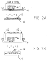
- Figs. 2A-B illustrate use of dual mode operation for depositing a metalization layer onto substrate 20.
- the elements corresponding to those shown in Fig. 1 are identified by like numbers.
- a low pressure deposition illustrated by Fig. 2A
- the range of motion of magnet assembly 22 is limited to the center area of the target and kept away from the edge of the target.
- more material 60 will tend to be deposited onto the central area of the substrate than on regions near the perimeter of the substrate.
- the pressure in the chamber is increased to levels that are appropriate for a high pressure deposition.
- a high pressure deposition is then performed in which the motion of the magnet assembly is extended out to the edge of the target as shown in Fig. 2B.
- the magnet assembly is allowed to spend a greater portion of its time near the outer region 62 of the target, then more material 62 will tend to be deposited near the perimeter of the substrate.
- the net result of the low pressure deposition followed by the high pressure deposition will be a more uniform metalization layer over the surface of the substrate.
- the substrate can be removed from the chamber after the low pressure deposition is complete and a shutter 50 (see Fig. 1) can be inserted between the target and the platform. Then a high pressure deposition can be performed onto the shutter for the purpose of "cleaning" the target and in general compensating for the nonuniform target erosion caused by the low pressure deposition.
- n th wafer e.g. the fifth or the tenth
- the high pressure mode of operation is then performed to clean and level the target.
- a small puck magnet assembly i.e., much smaller than the size of the target
- a more complex, larger magnet assembly such as is described U.S. Patent 5,242,566 by Norman W. Parker, entitled “Planar Magnetron Sputtering Source Enabling a Controlled Sputtering Profile Out to the Target Perimeter,” incorporated herein by reference.
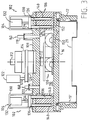
- an alternative approach which is illustrated in Fig. 3, uses two magnet assemblies - one magnet assembly produces the magnetic field for low pressure operation and the combination of the two magnet assemblies produces the magnetic field for high pressure operation.
- one of the magnet assemblies produces the magnetic field in the inner region of the face of the target and the other magnet assembly produces the magnetic field in the outer perimeter region of the face of the target.
- the magnet assembly which produces the field in the inner region is a rotating inner magnet assembly 100 and the magnet assembly which produces the magnetic field in the outer perimeter region is a non-rotating outer magnet assembly 102 that surrounds inner magnet assembly 100.
- Inner magnet assembly 100 is sized and configured so that as it rotates the magnetic field that it produces sweeps over the face of target 16 within the previously-mentioned inner region.
- Inner magnet assembly 100 can be of a known design such as, for example, are described in U.S. Patent 5,320,728 and in the previously-mentioned U.S. Patent 5,242,566, both of which are incorporated herein by reference.
- a cylindrical body 106 which has a top plate 108 covering its upper end, is mounted on top of target 16 and forms a cavity 110 which houses inner magnet assembly 100.
- a drive shaft 112 with its lower end coupled to inner magnet assembly 100 passes up through top plate 108 and has a pulley 114 mounted on its upper end.
- Top plate 108 also includes an inlet port 118 and an outlet port 120 through which coolant (e.g. water) is pumped into internal cavity 110 to cool inner magnet assembly 100 and target 16 during plasma sputtering.
- coolant e.g. water
- a grounded, generally cylindrically-shaped shield 19' surrounds the inside of the chamber and extends up close to target 16.
- the lower end of shield 19' includes an annular portion defining an opening through which sputtered material can pass to deposit onto the substrate (not shown).
- a motor 122 which is mounted above top plate 108, has its output shaft 124 coupled to pulley 114 through a drive belt 126 that is made of an electrically insulating material (e.g. rubber). Motor 122 rotates inner magnet assembly 100 during operation and drive belt 126 assures that inner magnet assembly 100 remains electrically isolated from motor 122.
- an electrically insulating material e.g. rubber
- a plurality of individual magnet subassemblies 104 which make up the larger outer non-rotating magnet assembly 102 are mounted at evenly spaced distances around the outer perimeter of top plate 108. In the described embodiment, which is for processing eight inch wafers, there are thirty such magnet subassemblies 104.
- Each of magnet assemblies 104 includes a U-shaped bracket 130 that holds a pneumatically operated solenoid 132 that raises and lowers a base plate 134 to which four vertically oriented rod magnets 136 are attached.
- the four rod magnets 136 of each magnet subassembly 104 are arranged at four corners of a rectangle as shown in Fig. 4.
- Holes 140 that are drilled through top plate 108 and into cylindrical body 106 are aligned with and receive rod magnets 136 when the individual magnet assemblies 104 are assembled onto top plate 108.
- there are four holes 140 for each magnet sub assembly 104 Two of the holes 140 are located along an inner circle 146 that is centered on the axis of drive shaft 112 and the remaining two holes are located long a larger outer circle 148 that is concentric with inner circle 146.
- solenoid 132 toggles between two positions, namely, a fully retracted position and a fully extended position.
- rod magnets 136 When the solenoid is in its fully retracted position, rod magnets 136 are pulled up towards solenoid 132 and further away from the face of target 16.
- rod magnets 136 When the solenoid is in its fully extended position, rod magnets 136 are pushed fully down into the holes so that their lowermost ends are close to the face of target 16.
- the high flux portion of the magnetic field that is produced by rod magnets 136 is in back of the target and does not significantly affect the sputtering process that is taking place at the face of the target.
- the high flux portion of the magnetic field that is produced by rod magnets In their fully extended positions, the high flux portion of the magnetic field that is produced by rod magnets is located right in front of the face of target 16 where it has maximum affect on the sputtering process that takes place there.
- the outer perimeter region has a radial width that is greater than about 1 mm.
- a width of about 25-50 mm is acceptable. It is desirable, however, to avoid making this outer perimeter region too wide, since that would result in less of the face of target 16 participating in the low pressure sputtering process.
- Rod magnets 136 are made of a strongly magnetic material. They can be made of any of a variety of commonly used materials such as ceramic, neodymium boron, or samarium cobalt, just to name a few. Rod magnets 136 can be made entirely of the magnetic material or alternatively they can be made of a steel bar with its lowermost end made of the magnetic material. It is also desirable, however, that the magnets that are used in inner magnet assembly 100 be made of the same type of material as that used in rod magnets 136. In other words, all magnets are selected to be equally strong so that there is less likelihood that one set of magnets will act to demagnetize the other set of magnets.
- base plates 134 are made of steel thereby forming a high magnetic permeability path for the magnetic flux from the rod magnets 136. This serves the important function of increasing the magnetic flux density between the free ends of the rod magnets.
- an alternative approach would be to raise and lower only the base plate and leave the rod magnets in a permanent lowered position with their ends close to the target.
- the base plate When the base plate is raised, it does not act as an effective shunt and the magnetic flux density near the face of the target would be attenuated.
- the base plate When the base plate is lowered, it acts as an effective shunt for the rod magnets and the magnetic flux density near the face of the target in the perimeter region would be enhanced.
- the solenoids of outer magnet assembly 102 are held in their fully retracted condition so that the magnetic field at the face of the target does not extend out to the edge of the target. If sputtering is allowed to take place under these conditions, the target will erode as shown by dashed line 150 in Fig. 3, i.e., the edge of the target will not erode significantly. To erode the edge of the target and thus to clean up the target, the solenoids are switched to their fully extended condition and sputtering is performed using higher chamber pressures, as previously described. In that case, the erosion pattern that will result from the outer magnet assembly is illustrated by dashed line 152. As should be apparent, by properly using these two modes of operation, it should be possible to achieve a relatively uniform face erosion of the target and to keep the target clean.
- the outer magnets should be lowered to clean the edge of the target depends on the process that is being performed in the chamber.
- One indicator of how frequently it should be used will be the particle contamination that is generated in the chamber. If particle contamination goes up, that is an indication that the magnets of the outer magnet assembly should be lowered more frequently for high pressure sputtering to clean the outer perimeter of the target. Typically, one might start by lowering the outer magnets once every 500 process runs. If it appears that particle contamination is increasing, then the magnets can be lowered more frequently.
- the plasma chambers described above and shown in Figs. 1 and 3 are merely illustrative.
- the dual mode magnetron sources that have been described can be used in a wide range of alternative deposition system configurations and designs.
- the deposition system might include additional power supplies, one of which could be used to bias the platform (and this the substrate) during processing.
- the power supplies could be RF supplies rather than D.C. supplies.
- the system can include many other features which are not shown in Fig. 1.
- the system might also include a robot for loading and removing wafers from the chamber, a lift mechanism for raising and lowering the pedestal, and a motor operated slit valve providing access to the inside of the chamber. Since such other features are of secondary importance with respect to the magnetron source, it is not necessary to describe them here in any greater detail.
Landscapes
- Chemical & Material Sciences (AREA)
- Engineering & Computer Science (AREA)
- Physics & Mathematics (AREA)
- Analytical Chemistry (AREA)
- Plasma & Fusion (AREA)
- Materials Engineering (AREA)
- Organic Chemistry (AREA)
- Metallurgy (AREA)
- Mechanical Engineering (AREA)
- Chemical Kinetics & Catalysis (AREA)
- Physical Vapour Deposition (AREA)
- Electrodes Of Semiconductors (AREA)
- Physical Deposition Of Substances That Are Components Of Semiconductor Devices (AREA)
Priority Applications (1)
| Application Number | Priority Date | Filing Date | Title |
|---|---|---|---|
| EP98109591A EP0877411A1 (de) | 1996-03-13 | 1997-03-11 | Magnetronquelle mit einer Magnetanordnung |
Applications Claiming Priority (2)
| Application Number | Priority Date | Filing Date | Title |
|---|---|---|---|
| US08/615,771 US5907220A (en) | 1996-03-13 | 1996-03-13 | Magnetron for low pressure full face erosion |
| US615771 | 1996-03-13 |
Related Child Applications (1)
| Application Number | Title | Priority Date | Filing Date |
|---|---|---|---|
| EP98109591A Division EP0877411A1 (de) | 1996-03-13 | 1997-03-11 | Magnetronquelle mit einer Magnetanordnung |
Publications (3)
| Publication Number | Publication Date |
|---|---|
| EP0801415A2 true EP0801415A2 (de) | 1997-10-15 |
| EP0801415A3 EP0801415A3 (de) | 1997-12-17 |
| EP0801415B1 EP0801415B1 (de) | 1999-12-08 |
Family
ID=24466743
Family Applications (2)
| Application Number | Title | Priority Date | Filing Date |
|---|---|---|---|
| EP97104017A Expired - Lifetime EP0801415B1 (de) | 1996-03-13 | 1997-03-11 | Magnetrongerät für ganzflächige Niederdruckerosion |
| EP98109591A Withdrawn EP0877411A1 (de) | 1996-03-13 | 1997-03-11 | Magnetronquelle mit einer Magnetanordnung |
Family Applications After (1)
| Application Number | Title | Priority Date | Filing Date |
|---|---|---|---|
| EP98109591A Withdrawn EP0877411A1 (de) | 1996-03-13 | 1997-03-11 | Magnetronquelle mit einer Magnetanordnung |
Country Status (6)
| Country | Link |
|---|---|
| US (2) | US5907220A (de) |
| EP (2) | EP0801415B1 (de) |
| JP (1) | JPH1036964A (de) |
| KR (1) | KR970067607A (de) |
| DE (1) | DE69700893T2 (de) |
| TW (1) | TW493011B (de) |
Families Citing this family (52)
| Publication number | Priority date | Publication date | Assignee | Title |
|---|---|---|---|---|
| US5907220A (en) * | 1996-03-13 | 1999-05-25 | Applied Materials, Inc. | Magnetron for low pressure full face erosion |
| GB9700158D0 (en) * | 1997-01-07 | 1997-02-26 | Gencoa Limited | Versatile coating deposition system |
| EP0918351A1 (de) * | 1997-11-19 | 1999-05-26 | Sinvaco N.V. | Flaches magnetron mit bewegbarer Magnetsanlage |
| US20030116427A1 (en) * | 2001-08-30 | 2003-06-26 | Applied Materials, Inc. | Self-ionized and inductively-coupled plasma for sputtering and resputtering |
| WO2003042424A1 (en) * | 2000-10-10 | 2003-05-22 | Applied Materials, Inc. | Self-ionized and inductively-coupled plasma for sputtering and resputtering |
| US10047430B2 (en) | 1999-10-08 | 2018-08-14 | Applied Materials, Inc. | Self-ionized and inductively-coupled plasma for sputtering and resputtering |
| US6610184B2 (en) * | 2001-11-14 | 2003-08-26 | Applied Materials, Inc. | Magnet array in conjunction with rotating magnetron for plasma sputtering |
| US8696875B2 (en) * | 1999-10-08 | 2014-04-15 | Applied Materials, Inc. | Self-ionized and inductively-coupled plasma for sputtering and resputtering |
| US8617351B2 (en) * | 2002-07-09 | 2013-12-31 | Applied Materials, Inc. | Plasma reactor with minimal D.C. coils for cusp, solenoid and mirror fields for plasma uniformity and device damage reduction |
| US8048806B2 (en) * | 2000-03-17 | 2011-11-01 | Applied Materials, Inc. | Methods to avoid unstable plasma states during a process transition |
| GB2377228C (en) * | 2000-07-27 | 2010-01-08 | Trikon Holdings Ltd | Magnetron sputtering |
| US6627050B2 (en) | 2000-07-28 | 2003-09-30 | Applied Materials, Inc. | Method and apparatus for depositing a tantalum-containing layer on a substrate |
| DE10122070B4 (de) * | 2001-05-07 | 2005-07-07 | Texas Instruments Deutschland Gmbh | Kathodenzerstäubungskammer zum Aufbringen von Material auf der Oberfläche einer in der Kammer befindlichen Halbleiterscheibe |
| US7374636B2 (en) * | 2001-07-06 | 2008-05-20 | Applied Materials, Inc. | Method and apparatus for providing uniform plasma in a magnetic field enhanced plasma reactor |
| JP4009087B2 (ja) * | 2001-07-06 | 2007-11-14 | アプライド マテリアルズ インコーポレイテッド | 半導体製造装置における磁気発生装置、半導体製造装置および磁場強度制御方法 |
| KR101179727B1 (ko) * | 2001-11-14 | 2012-09-04 | 어플라이드 머티어리얼스, 인코포레이티드 | 스퍼터링 및 재스퍼터링을 위한 자기-이온화 및 유도 결합 플라즈마 |
| US7041201B2 (en) * | 2001-11-14 | 2006-05-09 | Applied Materials, Inc. | Sidewall magnet improving uniformity of inductively coupled plasma and shields used therewith |
| US20030192646A1 (en) * | 2002-04-12 | 2003-10-16 | Applied Materials, Inc. | Plasma processing chamber having magnetic assembly and method |
| JP2004018896A (ja) * | 2002-06-13 | 2004-01-22 | Matsushita Electric Ind Co Ltd | スパッタ膜の成膜方法 |
| TWI283899B (en) * | 2002-07-09 | 2007-07-11 | Applied Materials Inc | Capacitively coupled plasma reactor with magnetic plasma control |
| US7504006B2 (en) * | 2002-08-01 | 2009-03-17 | Applied Materials, Inc. | Self-ionized and capacitively-coupled plasma for sputtering and resputtering |
| US6846396B2 (en) * | 2002-08-08 | 2005-01-25 | Applied Materials, Inc. | Active magnetic shielding |
| US7458335B1 (en) | 2002-10-10 | 2008-12-02 | Applied Materials, Inc. | Uniform magnetically enhanced reactive ion etching using nested electromagnetic coils |
| US7422654B2 (en) * | 2003-02-14 | 2008-09-09 | Applied Materials, Inc. | Method and apparatus for shaping a magnetic field in a magnetic field-enhanced plasma reactor |
| US7300558B2 (en) * | 2003-10-21 | 2007-11-27 | Seagate Technology Llc | Rapid cycle time gas burster |
| US7182843B2 (en) * | 2003-11-05 | 2007-02-27 | Dexter Magnetic Technologies, Inc. | Rotating sputtering magnetron |
| US7294224B2 (en) * | 2003-12-01 | 2007-11-13 | Applied Materials, Inc. | Magnet assembly for plasma containment |
| US20050266173A1 (en) * | 2004-05-26 | 2005-12-01 | Tokyo Electron Limited | Method and apparatus of distributed plasma processing system for conformal ion stimulated nanoscale deposition process |
| US7686928B2 (en) * | 2004-09-23 | 2010-03-30 | Applied Materials, Inc. | Pressure switched dual magnetron |
| WO2006085354A1 (ja) * | 2005-02-08 | 2006-08-17 | Tohoku Seiki Industries, Ltd. | スパッタリング装置 |
| US20070012557A1 (en) * | 2005-07-13 | 2007-01-18 | Applied Materials, Inc | Low voltage sputtering for large area substrates |
| US8361283B2 (en) * | 2005-07-28 | 2013-01-29 | Seagate Technology Llc | Method and apparatus for cleaning a target of a sputtering apparatus |
| US20080067058A1 (en) * | 2006-09-15 | 2008-03-20 | Stimson Bradley O | Monolithic target for flat panel application |
| EP2246459A1 (de) * | 2008-02-13 | 2010-11-03 | Shibaura Mechatronics Corporation | Magnetron-sputtergerät und magnetron-sputterverfahren |
| JP2009287076A (ja) * | 2008-05-28 | 2009-12-10 | Showa Denko Kk | スパッタリング方法及び装置 |
| US20100012481A1 (en) * | 2008-07-21 | 2010-01-21 | Guo G X | Deposition system having improved material utilization |
| DE102008050499B4 (de) | 2008-10-07 | 2014-02-06 | Systec System- Und Anlagentechnik Gmbh & Co. Kg | PVD-Beschichtungsverfahren, Vorrichtung zur Durchführung des Verfahrens und nach dem Verfahren beschichtete Substrate |
| JP5003667B2 (ja) * | 2008-12-15 | 2012-08-15 | 大日本印刷株式会社 | 薄膜の製造方法および薄膜製造装置 |
| CN102471878B (zh) | 2009-07-17 | 2013-11-20 | 株式会社爱发科 | 成膜装置 |
| WO2011098413A1 (en) * | 2010-02-10 | 2011-08-18 | Oc Oerlikon Balzers Ag | Magnetron source and method of manufacturing |
| US8699183B2 (en) | 2011-04-22 | 2014-04-15 | Seagate Technology Llc | Write pole and shield with different taper angles |
| JP2012251233A (ja) * | 2011-06-07 | 2012-12-20 | Sharp Corp | 成膜装置及び発光装置 |
| US10106883B2 (en) | 2011-11-04 | 2018-10-23 | Intevac, Inc. | Sputtering system and method using direction-dependent scan speed or power |
| CN104114741B (zh) * | 2011-11-04 | 2016-06-22 | 因特瓦克公司 | 线性扫描溅射系统和方法 |
| US8830625B2 (en) | 2012-11-29 | 2014-09-09 | Seagate Technology Llc | Data writer with tapered side shield sidewalls |
| KR20140085049A (ko) * | 2012-12-27 | 2014-07-07 | 삼성디스플레이 주식회사 | 자화 방지 스퍼터링 장치 및 그 구동 방법 |
| US10505412B2 (en) | 2013-01-24 | 2019-12-10 | Clearwater Holdings, Ltd. | Flux machine |
| US20140263179A1 (en) * | 2013-03-15 | 2014-09-18 | Lam Research Corporation | Tuning system and method for plasma-based substrate processing systems |
| KR20230004879A (ko) | 2014-07-23 | 2023-01-06 | 클리어워터 홀딩스, 엘티디. | 플럭스 장치 |
| EP3669391A4 (de) | 2017-09-08 | 2021-05-26 | Clearwater Holdings, Ltd. | Systeme und verfahren für verbesserte elektrische speicherung |
| EP3695493B1 (de) | 2017-10-29 | 2024-03-20 | Clearwater Holdings, Ltd. | Modulare elektromagnetische maschine |
| JP7831934B2 (ja) * | 2022-07-15 | 2026-03-17 | 東京エレクトロン株式会社 | 成膜装置及び成膜装置の制御方法 |
Family Cites Families (22)
| Publication number | Priority date | Publication date | Assignee | Title |
|---|---|---|---|---|
| FR2298880A1 (fr) * | 1975-01-22 | 1976-08-20 | Commissariat Energie Atomique | Procede et dispositif d'implantation ionique |
| US4309266A (en) * | 1980-07-18 | 1982-01-05 | Murata Manufacturing Co., Ltd. | Magnetron sputtering apparatus |
| US4500408A (en) * | 1983-07-19 | 1985-02-19 | Varian Associates, Inc. | Apparatus for and method of controlling sputter coating |
| US4581260A (en) * | 1984-09-25 | 1986-04-08 | Ampex Corporation | Electroless plating method and apparatus |
| US4714536A (en) * | 1985-08-26 | 1987-12-22 | Varian Associates, Inc. | Planar magnetron sputtering device with combined circumferential and radial movement of magnetic fields |
| DE4017111C2 (de) * | 1990-05-28 | 1998-01-29 | Hauzer Holding | Lichtbogen-Magnetron-Vorrichtung |
| US4902398A (en) * | 1988-04-27 | 1990-02-20 | American Thim Film Laboratories, Inc. | Computer program for vacuum coating systems |
| JPH02298024A (ja) * | 1989-05-12 | 1990-12-10 | Tadahiro Omi | リアクティブイオンエッチング装置 |
| US5635036A (en) * | 1990-01-26 | 1997-06-03 | Varian Associates, Inc. | Collimated deposition apparatus and method |
| ES2089039T3 (es) * | 1990-02-09 | 1996-10-01 | Applied Materials Inc | Procedimiento para la eliminacion de material excedente de una camara para la deposicion por chisporroteo y dispositivo para la realizacion del mismo. |
| US5320728A (en) * | 1990-03-30 | 1994-06-14 | Applied Materials, Inc. | Planar magnetron sputtering source producing improved coating thickness uniformity, step coverage and step coverage uniformity |
| EP0451642B1 (de) * | 1990-03-30 | 1996-08-21 | Applied Materials, Inc. | Zerstäubungssystem |
| US5242566A (en) * | 1990-04-23 | 1993-09-07 | Applied Materials, Inc. | Planar magnetron sputtering source enabling a controlled sputtering profile out to the target perimeter |
| DE4125110C2 (de) * | 1991-07-30 | 1999-09-09 | Leybold Ag | Magnetron-Zerstäubungskathode für Vakuumbeschichtungsanlagen |
| US5194131A (en) * | 1991-08-16 | 1993-03-16 | Varian Associates, Inc. | Apparatus and method for multiple ring sputtering from a single target |
| US5322606A (en) * | 1991-12-26 | 1994-06-21 | Xerox Corporation | Use of rotary solenoid as a shutter actuator on a rotating arm |
| DE4329155A1 (de) * | 1993-08-30 | 1995-03-02 | Bloesch W Ag | Magnetfeldkathode |
| US5496455A (en) * | 1993-09-16 | 1996-03-05 | Applied Material | Sputtering using a plasma-shaping magnet ring |
| JPH07166346A (ja) * | 1993-12-13 | 1995-06-27 | Ulvac Japan Ltd | マグネトロンスパッタリング装置 |
| JP2755138B2 (ja) | 1993-12-15 | 1998-05-20 | 日本電気株式会社 | スパッタ装置 |
| JP3100837B2 (ja) * | 1993-12-24 | 2000-10-23 | 松下電器産業株式会社 | スパッタリング装置 |
| US5907220A (en) * | 1996-03-13 | 1999-05-25 | Applied Materials, Inc. | Magnetron for low pressure full face erosion |
-
1996
- 1996-03-13 US US08/615,771 patent/US5907220A/en not_active Expired - Lifetime
-
1997
- 1997-03-11 EP EP97104017A patent/EP0801415B1/de not_active Expired - Lifetime
- 1997-03-11 TW TW086103016A patent/TW493011B/zh not_active IP Right Cessation
- 1997-03-11 DE DE69700893T patent/DE69700893T2/de not_active Expired - Fee Related
- 1997-03-11 EP EP98109591A patent/EP0877411A1/de not_active Withdrawn
- 1997-03-12 KR KR1019970008179A patent/KR970067607A/ko not_active Ceased
- 1997-03-13 JP JP9100742A patent/JPH1036964A/ja not_active Withdrawn
-
1999
- 1999-03-02 US US09/261,002 patent/US6228235B1/en not_active Expired - Lifetime
Also Published As
| Publication number | Publication date |
|---|---|
| EP0877411A1 (de) | 1998-11-11 |
| EP0801415B1 (de) | 1999-12-08 |
| DE69700893D1 (de) | 2000-01-13 |
| JPH1036964A (ja) | 1998-02-10 |
| KR970067607A (ko) | 1997-10-13 |
| US6228235B1 (en) | 2001-05-08 |
| TW493011B (en) | 2002-07-01 |
| US5907220A (en) | 1999-05-25 |
| DE69700893T2 (de) | 2000-07-20 |
| EP0801415A3 (de) | 1997-12-17 |
Similar Documents
| Publication | Publication Date | Title |
|---|---|---|
| US5907220A (en) | Magnetron for low pressure full face erosion | |
| KR100455494B1 (ko) | 불균일성을 보상하면서 표면을 물리적 기상 공정하는 장치 | |
| US6358376B1 (en) | Biased shield in a magnetron sputter reactor | |
| CN1324641C (zh) | 用于等离子体溅射的与旋转磁控管结合的磁体阵列 | |
| CN1154750C (zh) | 采用磁桶和同心等离子体源及材料源的离子化物理气相淀积装置 | |
| US5702573A (en) | Method and apparatus for improved low pressure collimated magnetron sputter deposition of metal films | |
| US20070012558A1 (en) | Magnetron sputtering system for large-area substrates | |
| EP0884761A1 (de) | Magnetron-Zerstäubungsvorrichtung mit rotierender Magnetanordnung | |
| WO2018140193A2 (en) | Extension of pvd chamber with multiple reaction gases, high bias power, and high power impulse source for deposition, implantation, and treatment | |
| US6013159A (en) | Particle trap in a magnetron sputtering chamber | |
| JPH073450A (ja) | 低圧動作用マグネトロンスパッタリングソース | |
| WO2000052734A1 (en) | Method and apparatus for ionized physical vapor deposition | |
| US6042706A (en) | Ionized PVD source to produce uniform low-particle deposition | |
| CN120591743A (zh) | 控制脉冲直流pvd形成的材料层中应力变化的方法及设备 | |
| JP2004506090A (ja) | 高圧物理気相堆積を実行する方法と装置 | |
| US7378001B2 (en) | Magnetron sputtering | |
| CA1204700A (en) | Magnetron reactive bias sputtering method and apparatus | |
| US20030116432A1 (en) | Adjustable throw reactor | |
| JPH10140346A (ja) | プラズマスパッタ装置 | |
| EP0848081A2 (de) | Verfahren und Vorrichtung zur physikalischen Dampfabscheidung | |
| US20190378699A1 (en) | Methods and apparatus for magnetron assemblies in semiconductor process chambers |
Legal Events
| Date | Code | Title | Description |
|---|---|---|---|
| PUAI | Public reference made under article 153(3) epc to a published international application that has entered the european phase |
Free format text: ORIGINAL CODE: 0009012 |
|
| AK | Designated contracting states |
Kind code of ref document: A2 Designated state(s): DE FR GB IT |
|
| PUAL | Search report despatched |
Free format text: ORIGINAL CODE: 0009013 |
|
| AK | Designated contracting states |
Kind code of ref document: A3 Designated state(s): DE FR GB IT |
|
| 17P | Request for examination filed |
Effective date: 19980616 |
|
| GRAG | Despatch of communication of intention to grant |
Free format text: ORIGINAL CODE: EPIDOS AGRA |
|
| 17Q | First examination report despatched |
Effective date: 19990209 |
|
| GRAG | Despatch of communication of intention to grant |
Free format text: ORIGINAL CODE: EPIDOS AGRA |
|
| GRAH | Despatch of communication of intention to grant a patent |
Free format text: ORIGINAL CODE: EPIDOS IGRA |
|
| GRAH | Despatch of communication of intention to grant a patent |
Free format text: ORIGINAL CODE: EPIDOS IGRA |
|
| GRAA | (expected) grant |
Free format text: ORIGINAL CODE: 0009210 |
|
| AK | Designated contracting states |
Kind code of ref document: B1 Designated state(s): DE FR GB IT |
|
| PG25 | Lapsed in a contracting state [announced via postgrant information from national office to epo] |
Ref country code: IT Free format text: LAPSE BECAUSE OF FAILURE TO SUBMIT A TRANSLATION OF THE DESCRIPTION OR TO PAY THE FEE WITHIN THE PRE;WARNING: LAPSES OF ITALIAN PATENTS WITH EFFECTIVE DATE BEFORE 2007 MAY HAVE OCCURRED AT ANY TIME BEFORE 2007. THE CORRECT EFFECTIVE DATE MAY BE DIFFERENT FROM THE ONE RECORDED.SCRIBED TIME-LIMIT Effective date: 19991208 Ref country code: FR Free format text: LAPSE BECAUSE OF FAILURE TO SUBMIT A TRANSLATION OF THE DESCRIPTION OR TO PAY THE FEE WITHIN THE PRESCRIBED TIME-LIMIT Effective date: 19991208 |
|
| REF | Corresponds to: |
Ref document number: 69700893 Country of ref document: DE Date of ref document: 20000113 |
|
| EN | Fr: translation not filed | ||
| PLBE | No opposition filed within time limit |
Free format text: ORIGINAL CODE: 0009261 |
|
| STAA | Information on the status of an ep patent application or granted ep patent |
Free format text: STATUS: NO OPPOSITION FILED WITHIN TIME LIMIT |
|
| 26N | No opposition filed | ||
| REG | Reference to a national code |
Ref country code: GB Ref legal event code: IF02 |
|
| PGFP | Annual fee paid to national office [announced via postgrant information from national office to epo] |
Ref country code: GB Payment date: 20020311 Year of fee payment: 6 |
|
| PGFP | Annual fee paid to national office [announced via postgrant information from national office to epo] |
Ref country code: DE Payment date: 20020328 Year of fee payment: 6 |
|
| PG25 | Lapsed in a contracting state [announced via postgrant information from national office to epo] |
Ref country code: GB Free format text: LAPSE BECAUSE OF NON-PAYMENT OF DUE FEES Effective date: 20030311 |
|
| PG25 | Lapsed in a contracting state [announced via postgrant information from national office to epo] |
Ref country code: DE Free format text: LAPSE BECAUSE OF NON-PAYMENT OF DUE FEES Effective date: 20031001 |
|
| GBPC | Gb: european patent ceased through non-payment of renewal fee |
Effective date: 20030311 |