EP0802417A2 - Halbleiterbeschleunigungsmesser - Google Patents
Halbleiterbeschleunigungsmesser Download PDFInfo
- Publication number
- EP0802417A2 EP0802417A2 EP97302664A EP97302664A EP0802417A2 EP 0802417 A2 EP0802417 A2 EP 0802417A2 EP 97302664 A EP97302664 A EP 97302664A EP 97302664 A EP97302664 A EP 97302664A EP 0802417 A2 EP0802417 A2 EP 0802417A2
- Authority
- EP
- European Patent Office
- Prior art keywords
- body member
- acceleration
- semiconductor
- support
- sensor
- Prior art date
- Legal status (The legal status is an assumption and is not a legal conclusion. Google has not performed a legal analysis and makes no representation as to the accuracy of the status listed.)
- Withdrawn
Links
- 239000004065 semiconductor Substances 0.000 title claims abstract description 113
- 230000001133 acceleration Effects 0.000 title claims abstract description 104
- 239000000758 substrate Substances 0.000 claims abstract description 41
- 230000004044 response Effects 0.000 claims abstract description 10
- 238000012935 Averaging Methods 0.000 claims abstract description 5
- 238000000034 method Methods 0.000 claims description 25
- 238000004519 manufacturing process Methods 0.000 claims description 18
- 230000005484 gravity Effects 0.000 claims description 11
- 238000005520 cutting process Methods 0.000 claims description 8
- 229910052751 metal Inorganic materials 0.000 claims description 7
- 239000002184 metal Substances 0.000 claims description 7
- 238000005304 joining Methods 0.000 claims description 5
- 230000005496 eutectics Effects 0.000 claims description 4
- 238000001514 detection method Methods 0.000 abstract description 15
- 230000035945 sensitivity Effects 0.000 description 21
- 238000012545 processing Methods 0.000 description 14
- 239000000853 adhesive Substances 0.000 description 9
- 230000001070 adhesive effect Effects 0.000 description 9
- PCHJSUWPFVWCPO-UHFFFAOYSA-N gold Chemical compound [Au] PCHJSUWPFVWCPO-UHFFFAOYSA-N 0.000 description 8
- 239000010931 gold Substances 0.000 description 8
- 229910052737 gold Inorganic materials 0.000 description 8
- 238000010586 diagram Methods 0.000 description 6
- XUIMIQQOPSSXEZ-UHFFFAOYSA-N Silicon Chemical compound [Si] XUIMIQQOPSSXEZ-UHFFFAOYSA-N 0.000 description 5
- 239000002245 particle Substances 0.000 description 5
- 230000009467 reduction Effects 0.000 description 5
- 229910052710 silicon Inorganic materials 0.000 description 5
- 239000010703 silicon Substances 0.000 description 5
- 238000005530 etching Methods 0.000 description 4
- 239000000463 material Substances 0.000 description 4
- 230000008569 process Effects 0.000 description 4
- 229910000679 solder Inorganic materials 0.000 description 4
- 239000000919 ceramic Substances 0.000 description 3
- 230000003014 reinforcing effect Effects 0.000 description 3
- 230000008901 benefit Effects 0.000 description 2
- 238000007906 compression Methods 0.000 description 2
- 238000006073 displacement reaction Methods 0.000 description 2
- 230000000694 effects Effects 0.000 description 2
- 238000009413 insulation Methods 0.000 description 2
- 230000008018 melting Effects 0.000 description 2
- 238000002844 melting Methods 0.000 description 2
- 238000005459 micromachining Methods 0.000 description 2
- 238000009966 trimming Methods 0.000 description 2
- ZOKXTWBITQBERF-UHFFFAOYSA-N Molybdenum Chemical compound [Mo] ZOKXTWBITQBERF-UHFFFAOYSA-N 0.000 description 1
- 230000003321 amplification Effects 0.000 description 1
- 238000007796 conventional method Methods 0.000 description 1
- 239000013078 crystal Substances 0.000 description 1
- 238000009713 electroplating Methods 0.000 description 1
- 239000011521 glass Substances 0.000 description 1
- QUCZBHXJAUTYHE-UHFFFAOYSA-N gold Chemical compound [Au].[Au] QUCZBHXJAUTYHE-UHFFFAOYSA-N 0.000 description 1
- 238000010438 heat treatment Methods 0.000 description 1
- 238000010348 incorporation Methods 0.000 description 1
- 239000007788 liquid Substances 0.000 description 1
- 229910052750 molybdenum Inorganic materials 0.000 description 1
- 239000011733 molybdenum Substances 0.000 description 1
- 238000003199 nucleic acid amplification method Methods 0.000 description 1
- 239000003921 oil Substances 0.000 description 1
- 230000007261 regionalization Effects 0.000 description 1
- 230000005476 size effect Effects 0.000 description 1
- 238000005476 soldering Methods 0.000 description 1
Images




Classifications
-
- G—PHYSICS
- G01—MEASURING; TESTING
- G01P—MEASURING LINEAR OR ANGULAR SPEED, ACCELERATION, DECELERATION, OR SHOCK; INDICATING PRESENCE, ABSENCE, OR DIRECTION, OF MOVEMENT
- G01P15/00—Measuring acceleration; Measuring deceleration; Measuring shock, i.e. sudden change of acceleration
- G01P15/02—Measuring acceleration; Measuring deceleration; Measuring shock, i.e. sudden change of acceleration by making use of inertia forces using solid seismic masses
- G01P15/08—Measuring acceleration; Measuring deceleration; Measuring shock, i.e. sudden change of acceleration by making use of inertia forces using solid seismic masses with conversion into electric or magnetic values
- G01P15/12—Measuring acceleration; Measuring deceleration; Measuring shock, i.e. sudden change of acceleration by making use of inertia forces using solid seismic masses with conversion into electric or magnetic values by alteration of electrical resistance
- G01P15/123—Measuring acceleration; Measuring deceleration; Measuring shock, i.e. sudden change of acceleration by making use of inertia forces using solid seismic masses with conversion into electric or magnetic values by alteration of electrical resistance by piezo-resistive elements, e.g. semiconductor strain gauges
Definitions
- the present invention relates to a semiconductor device including a semiconductor acceleration sensor which converts displacement into an electrical signal utilizing the piezoresistance effect of a semiconductor crystal such as silicon.
- Fig. 4 shows a semiconductor acceleration sensor produced by micromachining that is disclosed in Japanese Unexamined Patent Publication No. Hei. 1-302167.
- a cantilever 21 is formed with a groove 23 in the vicinity of a support 24 by etching, so that a thin portion 22 is formed there.
- Piezoresistors 2 formed on the top surface of the sensor constitute a bridge circuit.
- a weight 4 is provided at a tip portion of the cantilever.
- Japanese Examined Utility Model Publication No. Hei. 3-20780 discloses an example in which a metal weight is formed by electroplating.
- Fig.15 shows a semiconductor acceleration sensor disclosed in Japanese Unexamined Patent Publication No. Hei. 5-312827.
- a cantilever sensor element 1 is formed with a groove 23 in the vicinity of a support 24 by etching, so that a thin portion 22 is formed.
- Piezoresistors 2c, 2d, 2e, and 2f formed on the top surface of the sensor constitute a bridge circuit.
- the piezoresistors 2b and 2d which serve as reference resistors are disposed on the support 24.
- the piezoresistors 2a and 2c which serve as variable resistors for detecting the deformation amount of the thin portion 22 are so arranged as to be perpendicular to the reference resistors.
- the sensor element 1 of the cantilever When the sensor element 1 of the cantilever receives acceleration, it is displaced, so that the resistance values of the piezoresistors 2a and 2c increase. Differences between the resistances of the piezoresistors 2a and 2c and those of the reference resistors 2c and 2f cause a voltage corresponding to the acceleration. This voltage is supplied to a semiconductor integrated circuit substrate 110 that is provided externally via wires 116, which performs signal processing such as amplification of a very small voltage and temperature compensation.
- Fig. 16 shows an example disclosed in Japanese Unexamined Patent Publication No. Hei. 6-331647 in which a cantilever sensor element 1 is formed by micromachining.
- signal processing circuits 112 such as a detection circuit and an EEPROM are formed on a rim 113 that surrounds the cantilever of the sensor element 1, to compensate the output characteristics of the sensor.
- a set of piezoresistors for detecting acceleration which are provided on the surface constitute a bridge circuit as shown in Fig. 4.
- the sensitivities in directions (other-axes directions) other than the detection axis need to be reduced.
- no measures are taken to reduce the sensitivities in the other-axes directions.
- the sensitivities in the other-axes directions result from an inclination of the sensor element which is introduced when the sensor element is fixed to a base, a deviation between the centers of gravity of the weight and the sensor element, and other factors.
- weights 4 are provided on both top and bottom surfaces of a tip portion of a cantilever 21 of a sensor element so that the center of gravity of the two weights as a whole coincides with the center of the cantilever in the thickness direction. This indicates how important the positional relationship between the centers of gravity of the sensor element 1 and the weights 4 is.
- the weight 4 In the methods of adding the weight 4, the weight 4 needs to be disposed at the center of gravity of the sensor element having the piezoresistors. However a positional deviation of the weight 4 deteriorates the characteristics because torsional stress on the sensor element is increased and acceleration comes to be detected in directions other than the detection axis. This is other-axes sensitivity characteristic of the acceleration sensor. The acceleration detection in directions other than the detection axis is a cause of erroneous operation. As described above, as far as the characteristics of the acceleration sensor are concerned, it is necessary that the sensor element should not be influenced by torsion and the like.
- the weight is attached to an end portion of the sensor element with an adhesive or the like. This causes major problems that the number of manufacturing steps increases and that there may occur a positional deviation between the centers of gravity of the sensor element and the weight. It is important how to decrease a positional deviation of the weight from the sensor element.
- the semiconductor acceleration sensor to increase the functionality of the sensor, it is necessary to connect the semiconductor integrated circuit substrate 110 (Fig. 15) for signal processing to the output stage of the sensor.
- an output voltage from the acceleration sensor which is caused by displacement due to acceleration is severalmillivolts. Therefore, connection to an amplifier circuit 111 is highly necessary.
- the strain sensing portion consists of the piezoresistors, a temperature variation occurs. This necessitates a temperature compensation circuit.
- the sensor element 1 and the semiconductor integrated circuit substrate 110 for signal processing are disposed adjacent to each other and connected together by wire bonding. In this case, because a very small signal is picked up, there is a possibility that noise is superimposed on the signal through the wires 116.
- An object of the invention is to reduce this type of noise.
- Fig. 17 discloses an example in which a voltage variation occurring in piezoresistors of a cantilever sensor element due to acceleration is supplied to a semiconductor integrated circuit substrate 110 as a weight provided at the other end and incorporating an amplifier circuit, and signal processing is performed in the semiconductor integrated circuit substrate 110.
- the cantilever 2 and the semiconductor integrated circuit substrate 110 are connected to each other via bumps 3. This example is shown in Fig. 17. In this method, since the semiconductor integrated circuit substrate 110 deals with very small, high-frequency signals, noise is likely to occur.
- Japanese Unexamined Patent Publication No. Hei. 6-331647 discloses the example in which the signal processing circuit 112 is formed on the periphery of the sensor element 1.
- the cantilever as the sensor element 1 is formed by etching while the semiconductor integrated circuit on the periphery is protected from an etching liquid. This means an increase in the number of manufacturing steps, and is therefore an obstruction to cost reduction. There is an additional problem of a reduction in yield.
- the invention has been made to solve the above problems.
- a sensor element is constituted by providing acceleration detecting means on the two faces so as to be opposed to each other.
- the acceleration detecting means on each face is constituted of a bridge circuit, and outputs from the two faces are averaged, whereby torsional stress is reduced and the other-axis sensitivity characteristics of the acceleration sensor is made superior.
- the invention is intended to lower the cost by making the material of the conventionally used support unnecessary by using the semiconductor integrated circuit substrate as the support .
- a feature of the invention is therefore to reduce noise and attain high performance by directly joining together the sensor element and the semiconductor integrated circuit substrate for signal processing without using the wires or the like, as well as to lower the cost by using the semiconductor integrated circuit substrate as the support.
- the patterns can be formed on both surfaces (front and back surfaces) of a semiconductor substrate, weights are formed on both side faces perpendicular to the acceleration detecting faces, whereby the center-of-gravity positions of the sensor element and the weights can be made coincident with each other. This configuration prevents detection of acceleration from other axes.
- a sensor element is fixed such that a rectangular parallelepiped structural body including piezoresistors is directly fixed to a semiconductor integrated circuit substrate from a semiconductor wafer.
- the semiconductor integrated circuit substrate as the support 24 for supporting the sensor, it becomes possible to supply semiconductor devices which are resistant to noise, highly accurate, small in the number of parts, and inexpensive.
- a face of a rectangular parallelepiped sensor element having piezoresistors are connected to a semiconductor integrated circuit through bumps. This allows easy detection of horizontal acceleration.
- the invention provides a semiconductor acceleration sensor device having a body member including a sensor portion movable in response to a force of acceleration, sensing means for providing a signal representative of such movement, a support member separate from said body member, and means interconnecting said support to one end of said body member, wherein said sensing means are provided on two opposing faces of said sensor portion.
- the invention provides a semiconductor acceleration sensor device having a body member including a sensor portion movable in response to a force of acceleration, sensing means for providing a signal representative of such movement, a support member separate from said body member, and means interconnecting said support to one end of said body member, wherein said sensing means are provided on two separate regions on either side of the centre of gravity of said sensor portion.
- the invention provides a semiconductor acceleration sensor device having a body member including a sensor portion movable in response to a force of acceleration, sensing means for providing a signal representative of such movement, a support member separate from said body member, and means interconnecting said support to one end of said body member, wherein a weight is provided on said sensor portion on a face thereof perpendicular to, or non-parallel with, the intended direction of acceleration.
- the invention provides a method of manufacturing a semiconductor acceleration sensor, comprising the steps of:
- the invention provides a semiconductor acceleration sensor device having a body member including a sensor portion movable in response to a force of acceleration, sensing means for providing a signal representative of such movement, a support member separate from said body member, and means interconnecting said support to one end of said body member, wherein said support member is a planar substrate of an integrated circuit.
- the semiconductor acceleration sensor is a rectangular parallelepiped structural body that is cut out from a semiconductor wafer 10 (Fig. 2) and formed with piezoresistors 2, output terminals 8, etc.
- This structural body is hereinafter called a sensor element 1.
- the piezoresistors 2, the output terminals 8, etc. are patterned on the side faces of the sensor element 1; that is, the piezoresistors 2 and the output terminals 8 exist on both side faces.
- the piezoresistors 2 are p-type piezoresistors.
- Bumps 3 for outputting electrical signals are formed on the output terminals 8. In this embodiment, gold bumps 3 are formed.
- the bumps 3 on the output terminals 8 have a size of 0.1 x 0.08 mm and a height of 0. 1 mm.
- the semiconductor acceleration sensor is mainly composed of the sensor element 1, a base 5 for taking out electrical signals from the sensor element 1 and for supporting the sensor element 1, weights 4 for providing sensitivity, and a package 20.
- a manufacturing method will be described with reference to Figs. 2 and 3.
- the piezoresistors 2 and the output terminals 8 are patterned on the semiconductor wafer 10. Scribe lines for cutting out are formed. Further, the gold bumps 3 are formed on the output terminal 8 portions. The above steps are performed on both faces of the semiconductor wafer.
- a amplifier circuit, a temperature compensation circuit, and other circuits may be formed during the pattern formation in Fig. 2A.
- Weights 4 for imparting sensitivity to the sensor element 1 are added.
- the weights 4 are made of silicon because it is preferable that the weights 4 be made of a material having the same thermal expansion coefficient as silicon which is the material of the sensor element 1.
- a metal such as molybdenum may be used. It is preferable to use, as an adhesive for bonding, an adhesive whose thermal expansion coefficient is close to that of silicon.
- the structure in this state is placed on the base 5.
- wiring lines 6 are formed on the base 5.
- ceramics is used.
- the wiring lines are made of gold.
- the sensor element 1 is fixed to the base 5 with an adhesive (not shown).
- the wiring lines of the base 5 and the bumps 3 of the sensor element 1 are connected to each other through an anisotropic conductive film.
- the anisotropic conductive film is an adhesive in which small conductive particles are dispersed. With the anisotropic conductive film, particles are interposed between electrodes by thermo-compression bonding to establish electrical conduction there while insulation between adjacent electrodes is secured.
- the structure in which the sensor element 1 is attached to the base 5 is mounted on a board.
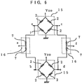
- the board is provided with an electrical circuit for picking up information from both side faces 100 of the sensor element 1 and eliminating dislocation due to torsional stress.
- This embodiment is so configured that a package 20 has functions of the substrate.
- the package 20 is made of ceramics. Resistors 2 for canceling other-axes sensitivities are formed on the circuit board.
- important items in the manufacturing process for obtaining a semiconductor acceleration sensor having superior characteristics are how to locate the weights 4 at the center of gravity of the sensor element 1 and how to obtain a high degree of orthogonality between the cutting (i.e., dicing) faces and the side faces having the piezoresistors 2 in the sensor element 1.
- dicing cutting
- the error variation component is reduced by a factor of 1/10.
- the resistance value of the resistors 6 be set five times or more that of the piezoresistors 2.
- electrical signals generated in the sensor element 1 are supplied to the board that is associated with the package via the electrodes of the base 5.
- the board is provided with the resistors 2 which are chip resistors in the embodiment.
- the electrical signals are finally supplied to output terminals 8 of the package via the chip resistors.
- FIG. 7 shows output results of be this embodiment.
- a data curve with marks "O" represents data obtained when the acceleration sensor was rotated. When the acceleration sensor receives gravitational acceleration, maximum output voltages are obtained at 0°, 180°, and 360°.
- the X axis that is the detection axis assumes a sine curve.
- a Z-axis sensitivity curve with marks "A” represents data obtained when the acceleration sensor is rotated with the piezoresistor sides directed to the gravity direction. Ideally, the Z-axis sensitivity should not cause any output.
- the output sensitivity of the detection axis was 2 V at 180° and 360°, while the data obtained when the acceleration sensor made one rotation with the faces having the piezoresistors 2 directed to the gravitational acceleration direction had an output sensitivity of 20 mV, which is 1 % of the output sensitivity of the output sensitivity axis and is superior as the other-axis sensitivity characteristic.
- Fig. 8 shows values obtained when the circuit processing of this embodiment was not performed.
- the other-axis sensitivity value is 10%, which means that the electrical circuit processing of this invention is effective.
- the other-axis sensitivity characteristics in a case of apparatuses which perform image processing based on angle detection, such as virtual reality apparatuses, detection of acceleration in an unnecessary direction may cause a problem such as an erroneous operation in which an image moves obliquely poor other-axis sensitivity characteristics may cause an erroneous operation also in a case of lifesaving means such as an air-bag.
- the semiconductor acceleration sensor is a rectangular parallelepiped structural body that is cut out from a semiconductor wafer 10 (Fig. 2) and formed with piezoresistors 2, output terminals 8, etc.
- the piezoresistors 2, the output terminals 8, etc. are patterned on the side faces of the sensor element 1.
- metal that will become the piezoresistors 2, bumps 3, and weights 4 in the process are formed on both surfaces of the semiconductor 10.
- the sensor element 1 is taken by cutting it out with a dicing machine.
- the sensor element 1 is configured such that its side faces are formed with the piezoresistors, output terminals 8, and weights 4.
- the weights are formed by a method that is similar to a method of forming the bumps 3 used for the output terminals 8. Although gold is formed by gilding, soldering may be used.
- the length is 10 mm (sensor portion: 7 mm; support: 3 mm), the width w is 0.6 mm, and the thickness is 0.25 mm.
- the shape of the weights formed on both side faces the length is 4 mm, the width is 0.2 mm, and the height is 0.02 mm.
- the weights weigh 2.4 mg. It is noted that the silicon cantilever portion weighs 1.8 mg and the gold bumps serve as weights of 0.6 mg.
- the piezoresistors are p-type piezoresistors 2.
- the bumps 3 for outputting electrical signals are formed on the output terminals 8.
- a cutting method by dicing according to the invention will be described below with reference to Figs. 11. Where bumps exist on both surfaces of a semiconductor wafer, chippings occur in cutting elements by dicing. Chippings are remarkable particularly on the fixed side.
- a dicing jig 201 was produced to lower the degree of chippings, Fig 11A.
- the jig is a flat plate having recessed portions. Fixing is effected in a state that the gold bumps of the output terminals 8 and the weight portion are inserted in the recesses, Fig. 11B.
- the semiconductor wafer 10 is fixed to the dicing jig 201 with wax. Since the semiconductor wafer is fixed by this method, sensor elements can be cut out without causing chippings.
- This method is very efficient because no labor is needed to mount weights in a later step. Further, where the piezoresistors as the detecting section are formed on the side faces with respect to the faces that are directed to the acceleration direction, it is advantageous in being capable of providing a configuration that is hardly affected from other axes.
- Fig. 12 shows an output voltage characteristic measured For 30 G, an output voltage of 0.15 mV/G was obtained.
- This method realizes an acceleration sensor which can be manufactured easily, though the method is a simple one in which the weights are formed on both side faces with respect to the faces for receiving acceleration.
- a rectangular parallelepiped body is formed with piezoresistors 2, output terminals , etc. which body is cut out from a semiconductor wafer 10 (Fig. 2). This body is hereinafter called a sensor element.
- a weight 4 is bonded to the sensor element 1.
- Bumps 3 for making electrical contact with a support 24 are formed on the output terminals.
- the bumps 3 are gold or solder bumps 3.
- Piezoresistors 2 and output terminals 8 are patterned on the surfaces of a semiconductor wafer 10 in Fig. 19A, and then the semiconductor wafer 10 is so cut that the piezoresistors 2 and the output terminals 8 exist in the same plane. Thus, a rectangular parallelepiped sensor element 1 in Fig. 19B is obtained. Finally, weights 4 are bonded to the rectangular parallelepiped sensor element 1 in Fig 19C.
- the semiconductor wafer 10 may be cut by dicing. The dicing is performed such that lines along which to scribe the sensor element 1 are formed to define its outline, and the semiconductor wafer 10 is cut by dicing with the scribe lines used as a reference.
- the semiconductor sensors 1 are arranged in the semiconductor wafer 25.
- acceleration sensors for low acceleration are used for earthquake detection, virtual reality, etc.
- the sensor element 1 formed with the weights 4 is fixed to a support 24 that is constituted of a semiconductor integrated circuit substrate 110. Since the output voltage of the sensor element 1 formed with the weights 4 is small, the semiconductor integrated circuit substrate 110 is given a signal processing function such as an amplifier circuit 112. Terminals are formed on the semiconductor integrated circuit substrate 10 to fix the sensor element 1 to the semiconductor integrated circuit substrate 110 as well as to take electrical contact between the bumps 3 of the output terminals 8 of the sensor element 1 and the semiconductor integrated circuit element 110.
- the sensor element 1 is composed of the portion that swings in response to acceleration and the fixed portion. To avoid influences of torsion and the like, a base may be attached to the fixed portion to reinforce it. In this embodiment, a reinforcing base 138 is used.
- the joining method electrical connections are established by a method using an anisotropic conductive film 120.
- the anisotropic conductive film 120 is an adhesive in which small conductive particles are dispersed. Through thermo-compression bonding, particles are interposed between electrodes to establish electrical conduction while insulation between adjacent electrodes is secured. Further, mechanical joining is effected when the adhesive sets. According to this method, conduction between the bumps 3 of the output terminals 8 of the sensor element 1 and the terminals of the semiconductor integrated circuit substrate 10 as the support 24 is obtained.
- Figs. 18 include front views on the left-hand side and side views on the right-hand side.
- an anisotropic film 120 is bonded to the output terminals 8 of the semiconductor integrated circuit substrate 110.
- the anisotropic conductive film 110 may be used to fix the reinforcing base to a land that is provided in the semiconductor integrated circuit.
- Fig. 18B the sensor element 1 is mounted from above so that the bumps 3 of the sensor element 1 are opposed to the output terminals 8 of the semiconductor integrated circuit substrate 110, and weight, which is about 100 kgf/cm for the bump 3, is applied from above the sensor element 1.
- weight which is about 100 kgf/cm for the bump 3.
- the anisotropic conductive film 120 is completely fixed and electrical connections between the sensor element 1 and the semiconductor integrated circuit are obtained.
- Fig. 18C shows a state that the electrical connections are obtained.
- connection is effected by gold-gold eutectic connection.
- solder bumps 3 the bumps 3 of the output terminals 8 of the sensor element 1 are opposed to the semiconductor integrated circuit substrate 110.
- the base is temporarily fixed, in advance, to the land of the semiconductor integrated circuit substrate 10.
- eutectic connection is effected by pressurizing and heating at 500°C.
- the semiconductor integrated circuit substrate 110 thus produced is packaged in a case 115 as shown in Fig. 14.
- the case 115 is made of ceramics, plastic, or the like.
- This embodiment uses a case 15 that enables surface mounting.
- a lid is provided on the surface.
- This embodiment uses a glass lid, to allow passage of laser light for trimming (the semiconductor integrated circuit substrate 10 has trimming circuits) .
- oil is injected to improve impact resistance and frequency characteristics.
- This embodiment uses the rectangular parallelepiped sensor element 1. As a result, horizontal acceleration can easily be detected by fixing the sensor element 1 to the semiconductor integrated circuit substrate 110. Where the sensor is used in a vehicle, for instance, in an air-bag system for impact detection, the above structure provides the greatest advantage that there is no need for cumbersome work such as a consideration of the mounting method, because the sensor is directed to the detecting direction.
- the characteristics of the sensor element 1 noise has been reduced as compared to the conventional method in which the sensor element is connected to the external semiconductor integrated circuit 110 for signal processing. Further, the incorporation of the semiconductor integrated circuit substrate 10 for signal processing in the case 115 has provided a size merit.
- the semiconductor integrated circuit substrate 10 for signal processing also serves as the support 24 rather than is provided externally as in the conventional case, and is connected to the sensor element 1 through the bumps 3.
- the semiconductor acceleration sensor of the invention was mounted in a vehicle, that is, used as an air-bag-operating sensor for lifesaving at the time of collision, the desired characteristics were obtained and the sensor was well within the range suitable for actual use.
Landscapes
- Physics & Mathematics (AREA)
- General Physics & Mathematics (AREA)
- Pressure Sensors (AREA)
- Micromachines (AREA)
Applications Claiming Priority (7)
| Application Number | Priority Date | Filing Date | Title |
|---|---|---|---|
| JP9889096 | 1996-04-19 | ||
| JP98890/96 | 1996-04-19 | ||
| JP121953/96 | 1996-05-16 | ||
| JP12195396 | 1996-05-16 | ||
| JP09023060A JP3117925B2 (ja) | 1996-04-19 | 1997-02-05 | 半導体加速度センサ |
| JP23060/97 | 1997-02-05 | ||
| US08/844,323 US6006606A (en) | 1996-04-19 | 1997-04-18 | Semiconductor acceleration sensor |
Publications (2)
| Publication Number | Publication Date |
|---|---|
| EP0802417A2 true EP0802417A2 (de) | 1997-10-22 |
| EP0802417A3 EP0802417A3 (de) | 1998-10-14 |
Family
ID=27457891
Family Applications (1)
| Application Number | Title | Priority Date | Filing Date |
|---|---|---|---|
| EP97302664A Withdrawn EP0802417A3 (de) | 1996-04-19 | 1997-04-18 | Halbleiterbeschleunigungsmesser |
Country Status (4)
| Country | Link |
|---|---|
| US (1) | US6006606A (de) |
| EP (1) | EP0802417A3 (de) |
| JP (1) | JP3117925B2 (de) |
| CN (1) | CN1172250A (de) |
Cited By (1)
| Publication number | Priority date | Publication date | Assignee | Title |
|---|---|---|---|---|
| US6006606A (en) * | 1996-04-19 | 1999-12-28 | Seiko Instruments R&D Center Inc. | Semiconductor acceleration sensor |
Families Citing this family (7)
| Publication number | Priority date | Publication date | Assignee | Title |
|---|---|---|---|---|
| JP2000097707A (ja) * | 1998-09-18 | 2000-04-07 | Fujitsu Ltd | 加速度センサ |
| US7302856B2 (en) * | 2003-05-07 | 2007-12-04 | California Institute Of Technology | Strain sensors based on nanowire piezoresistor wires and arrays |
| US7552645B2 (en) * | 2003-05-07 | 2009-06-30 | California Institute Of Technology | Detection of resonator motion using piezoresistive signal downmixing |
| US7434476B2 (en) * | 2003-05-07 | 2008-10-14 | Califronia Institute Of Technology | Metallic thin film piezoresistive transduction in micromechanical and nanomechanical devices and its application in self-sensing SPM probes |
| TWI220141B (en) * | 2003-08-05 | 2004-08-11 | Ind Tech Res Inst | Performance adjusting apparatus for inertia sensor |
| JP4697004B2 (ja) | 2006-03-29 | 2011-06-08 | 株式会社日立製作所 | 力学量測定装置 |
| JP5135824B2 (ja) * | 2007-02-21 | 2013-02-06 | パナソニック株式会社 | 慣性力センサ素子の製造方法 |
Family Cites Families (10)
| Publication number | Priority date | Publication date | Assignee | Title |
|---|---|---|---|---|
| US5000817A (en) * | 1984-10-24 | 1991-03-19 | Aine Harry E | Batch method of making miniature structures assembled in wafer form |
| JPH0821722B2 (ja) * | 1985-10-08 | 1996-03-04 | 日本電装株式会社 | 半導体振動・加速度検出装置 |
| US4891982A (en) * | 1986-06-27 | 1990-01-09 | Sundstrand Data Control, Inc. | Temperature compensation of a steady-state accelerometer |
| EP0456285A3 (en) * | 1986-09-22 | 1992-01-02 | Nippondenso Co., Ltd. | Semiconductor accelerometer |
| US5343064A (en) * | 1988-03-18 | 1994-08-30 | Spangler Leland J | Fully integrated single-crystal silicon-on-insulator process, sensors and circuits |
| US4969359A (en) * | 1989-04-06 | 1990-11-13 | Ford Motor Company | Silicon accelerometer responsive to three orthogonal force components and method for fabricating |
| JPH0830716B2 (ja) * | 1990-11-30 | 1996-03-27 | 三菱電機株式会社 | 半導体加速度検出装置 |
| WO1992015018A1 (en) * | 1991-02-14 | 1992-09-03 | Endevco Corporation | Piezoresistive accelerometer and method of fabrication |
| JP3114006B2 (ja) * | 1994-08-29 | 2000-12-04 | セイコーインスツルメンツ株式会社 | 半導体装置、及び、その製造方法 |
| JP3117925B2 (ja) * | 1996-04-19 | 2000-12-18 | 株式会社エスアイアイ・アールディセンター | 半導体加速度センサ |
-
1997
- 1997-02-05 JP JP09023060A patent/JP3117925B2/ja not_active Expired - Fee Related
- 1997-04-18 CN CN97113221.6A patent/CN1172250A/zh active Pending
- 1997-04-18 US US08/844,323 patent/US6006606A/en not_active Expired - Fee Related
- 1997-04-18 EP EP97302664A patent/EP0802417A3/de not_active Withdrawn
Cited By (1)
| Publication number | Priority date | Publication date | Assignee | Title |
|---|---|---|---|---|
| US6006606A (en) * | 1996-04-19 | 1999-12-28 | Seiko Instruments R&D Center Inc. | Semiconductor acceleration sensor |
Also Published As
| Publication number | Publication date |
|---|---|
| EP0802417A3 (de) | 1998-10-14 |
| JP3117925B2 (ja) | 2000-12-18 |
| CN1172250A (zh) | 1998-02-04 |
| JPH1032341A (ja) | 1998-02-03 |
| US6006606A (en) | 1999-12-28 |
Similar Documents
| Publication | Publication Date | Title |
|---|---|---|
| US5864063A (en) | Electrostatic capacity-type acceleration sensor | |
| US7578162B2 (en) | Apparatus for detecting a physical quantity acting as an external force and method for testing and manufacturing this apparatus | |
| CN100565211C (zh) | 半导体型三轴加速度传感器 | |
| US6158283A (en) | Semiconductor acceleration sensor | |
| EP3534126B1 (de) | Messvorrichtung, insbesondere eine lastmessvorrichtung | |
| JPH04301575A (ja) | 加速度計デバイス | |
| US6005275A (en) | Semiconductor acceleration sensor with cantilever | |
| US6006606A (en) | Semiconductor acceleration sensor | |
| JP2005180930A (ja) | 半導体センサ装置及びその製造方法 | |
| JPH07325104A (ja) | 加速度センサ | |
| KR20030039367A (ko) | 가속도 센서 | |
| EP1342988A2 (de) | Kapazitiver Sensor | |
| US6060780A (en) | Surface mount type unit and transducer assembly using same | |
| JPH11211750A (ja) | 半導体センサおよび半導体センサ用パッケージ | |
| JPH0660906B2 (ja) | 半導体加速度センサ | |
| JP2020113626A (ja) | 半導体装置およびその製造方法 | |
| US4987780A (en) | Integrated accelerometer assembly | |
| JP4839826B2 (ja) | センサモジュール | |
| JP3034620B2 (ja) | 三次元加速度センサ | |
| US5821595A (en) | Carrier structure for transducers | |
| JP4715503B2 (ja) | センサモジュールの製造方法 | |
| EP0793103A2 (de) | Halbleiter-Beschleunigungssensor | |
| US20260009818A1 (en) | Physical Quantity Sensor And Physical Quantity Detection Device | |
| US20260062285A1 (en) | Transducer | |
| JP4706634B2 (ja) | 半導体センサおよびその製造方法 |
Legal Events
| Date | Code | Title | Description |
|---|---|---|---|
| PUAI | Public reference made under article 153(3) epc to a published international application that has entered the european phase |
Free format text: ORIGINAL CODE: 0009012 |
|
| AK | Designated contracting states |
Kind code of ref document: A2 Designated state(s): DE FR IT |
|
| PUAL | Search report despatched |
Free format text: ORIGINAL CODE: 0009013 |
|
| AK | Designated contracting states |
Kind code of ref document: A3 Designated state(s): DE FR IT |
|
| 17P | Request for examination filed |
Effective date: 19990414 |
|
| STAA | Information on the status of an ep patent application or granted ep patent |
Free format text: STATUS: THE APPLICATION HAS BEEN WITHDRAWN |
|
| 18W | Application withdrawn |
Withdrawal date: 19990527 |