EP0802572B1 - Indicateur de mode d'operation avec source lumineuse montée en surface - Google Patents
Indicateur de mode d'operation avec source lumineuse montée en surface Download PDFInfo
- Publication number
- EP0802572B1 EP0802572B1 EP97106059A EP97106059A EP0802572B1 EP 0802572 B1 EP0802572 B1 EP 0802572B1 EP 97106059 A EP97106059 A EP 97106059A EP 97106059 A EP97106059 A EP 97106059A EP 0802572 B1 EP0802572 B1 EP 0802572B1
- Authority
- EP
- European Patent Office
- Prior art keywords
- housing
- resistor
- series resistor
- light
- lighting element
- Prior art date
- Legal status (The legal status is an assumption and is not a legal conclusion. Google has not performed a legal analysis and makes no representation as to the accuracy of the status listed.)
- Expired - Lifetime
Links
Images
Classifications
-
- H—ELECTRICITY
- H10—SEMICONDUCTOR DEVICES; ELECTRIC SOLID-STATE DEVICES NOT OTHERWISE PROVIDED FOR
- H10H—INORGANIC LIGHT-EMITTING SEMICONDUCTOR DEVICES HAVING POTENTIAL BARRIERS
- H10H20/00—Individual inorganic light-emitting semiconductor devices having potential barriers, e.g. light-emitting diodes [LED]
- H10H20/80—Constructional details
- H10H20/85—Packages
- H10H20/8506—Containers
-
- H—ELECTRICITY
- H10—SEMICONDUCTOR DEVICES; ELECTRIC SOLID-STATE DEVICES NOT OTHERWISE PROVIDED FOR
- H10W—GENERIC PACKAGES, INTERCONNECTIONS, CONNECTORS OR OTHER CONSTRUCTIONAL DETAILS OF DEVICES COVERED BY CLASS H10
- H10W90/00—Package configurations
-
- H—ELECTRICITY
- H10—SEMICONDUCTOR DEVICES; ELECTRIC SOLID-STATE DEVICES NOT OTHERWISE PROVIDED FOR
- H10W—GENERIC PACKAGES, INTERCONNECTIONS, CONNECTORS OR OTHER CONSTRUCTIONAL DETAILS OF DEVICES COVERED BY CLASS H10
- H10W90/00—Package configurations
- H10W90/701—Package configurations characterised by the relative positions of pads or connectors relative to package parts
- H10W90/751—Package configurations characterised by the relative positions of pads or connectors relative to package parts of bond wires
- H10W90/756—Package configurations characterised by the relative positions of pads or connectors relative to package parts of bond wires between a chip and a stacked lead frame, conducting package substrate or heat sink
Definitions
- the invention relates to an operating state display with a housing in which a surface-mounted device (SMD) light-emitting diode as a lighting element and arranged next to a series resistor are integrated.
- SMD surface-mounted device
- LEDs are nowadays usually manufactured in different brightness groups and combined in groups of double brightness.
- US 5,003,357 describes a semiconductor light-emitting element having a surface-mounted device housing with a lighting element and a light-emitting diode chip with a series resistor.
- Patent Abstracts of Japan JP 05347434 describes a light-emitting element with a housing, on the underside of which a resistor is arranged.
- EP 560 605 A1 describes a light source with an LED chip which is arranged on a carrier.
- a resistive element is arranged, both the resistive element and the LED are arranged in series in SMD construction on the support side by side.
- a light emitting diode is provided as a lighting element and a laser tunable series resistor, which is integrated in the housing next to the light emitting diode and serves to adjust the brightness of the light emitting diode.
- Connection contacts are arranged on both narrow sides of the rectangular housing, and the heat generated in the series resistor is dissipated by means of convection through the ambient air through a ventilation opening in the housing below the series resistor.
- the lighting element according to the invention which is formed by the light-emitting diode with integrated resistor, eliminates the cost of the storage since then and the significant assembly costs, since now only one component is to be mounted, where previously at least two parts were to be mounted. This also eliminates the creation of different bills of material.
- a reduction in the sanctity tolerance to less than the previously customary value 2.0 is connected, preferably to ⁇ 1.5, whereby at several together mounted lighting elements the
- the illumination element according to the invention is designed as a ("surface mounted device” (SMD), which takes up very little space during assembly, wherein the pre-resistor housed in the housing of the light-emitting diode series resistor is designed to be compact.
- SMD surface mounted device
- the housing forms a multiple of a basic design
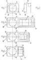
- Fig. 1 is a conventional lighting element 10 according to the invention with a housing 12 having an LED chip 14 disposed therein and associated therewith terminal contacts 15, 17, which include the housing 12 on both sides with respect to the near-surface mounting as an SMD component.
- the housing 12 of the lighting element 10 is formed as a so-called tantalum B or PLCC 2 housing. This has the advantage that the dimensions of theInternetelemnts are quasi-normalized, regardless of the respective applied supply voltage.
- Serving as a light source LED chip 14 is covered in an introduced into the housing 10 deck-side cutout 18 with a transparent potting compound.
- FIG. 2 shows a side view of the illumination element 10 shown in plan view in FIG. 1, whereby the size ratios of the top surface on the one hand and the component thickness can be seen on the basis of this illustration.
- a first lighting element 20 which has a housing 22 similar to the tantalum B design.
- the housing 22 is compared to the size shown in Fig. 1 by about two and a half times larger, the additional space next to the arranged therein LED 24 for receiving an integrated series resistor 26 is used.
- terminal contacts 25, 27 are in turn arranged.
- the light-emitting diode 24 radiates outwardly through a circular recess 28 formed in the housing 22, the resistor arranged next to it is designed as a laser-tunable resistor, so that the resistance required for the light-emitting diode 24 was worth can be adjusted individually with regard to the voltage applied in the application.
- FIG. 4 a similar arrangement, as shown in Fig. 3, with a second illumination element 30 with a housing 32, with an LED chip 34 and a series resistor 36 is shown, wherein, however, the resistor 36 has smaller dimensions than the resistor 26 in Fig. 3.
- 32 terminal contacts 35, 37 are arranged at the ends of the likewise rectangular housing.
- a round recess 38 is likewise formed on the upper side of the housing 32.
- a variant of a lighting element 40 is shown, which is slightly smaller than that shown in Fig. 4 lighting element 30, in which case, however, the arranged next to the light emitting diode 44 series resistor 46 is mounted swiveled by 90 °.
- the illumination element 40 according to the invention is possible with otherwise identical performance data.
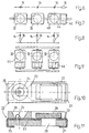
- Fig. 6 Shown in Fig. 6 is a first circuit example of a conventional series connection of three light-emitting diodes 14 and a series resistor 16, as is commonly used.
- FIG. 8 shows a second circuit example for a conventional parallel connection of three light-emitting diodes 14 and their associated series resistors 16.
- FIG. 9 shows a parallel circuit corresponding to that shown in FIG. 8, which is realized with the lighting elements 40. Since in this case the associated series resistor 46 is integrated in each case in the housing 42 of the lighting element 40 together with the LED chip 44, resulting now only three Parts to be assembled, that is, the required assembly costs are reduced by half.
- an inventive lighting element 20 is shown in plan view, so that both the LED chip 24 and the associated resistor 26 and the contact track 23 to each other and the terminal contacts 25, 27 can be seen.
- Fig. 11 shows the arrangement shown in Fig. 10 in longitudinal section from the side.
- the series resistor 26 the contact track 23 and terminal contacts 25, 27 and the recess 28, a ventilation opening 29 can be seen on the underside below the dropping resistor 26.
- heat generated in the series resistor 26 can be removed by means of convection by the ambient air. As a result, a better power utilization is possible.
Landscapes
- Illuminated Signs And Luminous Advertising (AREA)
- Led Device Packages (AREA)
- Led Devices (AREA)
- Arrangement Of Elements, Cooling, Sealing, Or The Like Of Lighting Devices (AREA)
Claims (1)
- Indicateur d'état de fonctionnement comprenant un élément lumineux (20) comportant un boitier (22) rectangulaire du type dispositif monté en surface (SMD), dans lequel sont intégrées une puce à diode électroluminescente (24) et une résistance série (26) agencée à coté de celle-ci, caractérisé en ce qu'il est prévu comme résistance série (26) une résistance ajustable par laser, des contacts de raccordement (25, 27) étant disposés sur les deux petits cotés du boîtier rectangulaire (22) et la chaleur produite dans la résistance série est évacuée par convection par l'air ambiant à travers une ouverture d'aération (29) ménagée dans le boitier (22) en dessous de la résistance série (26).
Applications Claiming Priority (2)
| Application Number | Priority Date | Filing Date | Title |
|---|---|---|---|
| DE19615839 | 1996-04-20 | ||
| DE19615839A DE19615839A1 (de) | 1996-04-20 | 1996-04-20 | SMD-Leuchtdiode |
Publications (3)
| Publication Number | Publication Date |
|---|---|
| EP0802572A2 EP0802572A2 (fr) | 1997-10-22 |
| EP0802572A3 EP0802572A3 (fr) | 2000-03-29 |
| EP0802572B1 true EP0802572B1 (fr) | 2006-04-05 |
Family
ID=7791978
Family Applications (1)
| Application Number | Title | Priority Date | Filing Date |
|---|---|---|---|
| EP97106059A Expired - Lifetime EP0802572B1 (fr) | 1996-04-20 | 1997-04-14 | Indicateur de mode d'operation avec source lumineuse montée en surface |
Country Status (2)
| Country | Link |
|---|---|
| EP (1) | EP0802572B1 (fr) |
| DE (2) | DE19615839A1 (fr) |
Families Citing this family (5)
| Publication number | Priority date | Publication date | Assignee | Title |
|---|---|---|---|---|
| DE102004003929B8 (de) * | 2004-01-26 | 2016-03-10 | Dominant Opto Technologies Sdn Bhd | Mit SM-Technologie bestückbares optoelektronisches Bauelement |
| DE102004003928B4 (de) * | 2004-01-26 | 2012-02-23 | Tay Kheng Chiong | Ein miniaturisiertes mit SM-Technologie bestückbares optoelektronisches Bauelement und Verfahren zur Herstellung dieses Bauelements |
| DE102006015335B4 (de) | 2006-04-03 | 2013-05-02 | Ivoclar Vivadent Ag | Halbleiter-Strahlungsquelle sowie Lichthärtgerät |
| DE102008058494A1 (de) * | 2008-11-21 | 2010-05-27 | Neumüller Elektronik GmbH | Anschlussfertiger LED-Modulkörper |
| DE102012211828B4 (de) | 2012-07-06 | 2023-03-02 | Lisa Dräxlmaier GmbH | LED-Beleuchtung für Fahrzeuge |
Citations (4)
| Publication number | Priority date | Publication date | Assignee | Title |
|---|---|---|---|---|
| JPS63138788A (ja) * | 1986-12-01 | 1988-06-10 | Ricoh Co Ltd | Ledアレイ |
| JPH0231457A (ja) * | 1988-07-21 | 1990-02-01 | Matsushita Electric Ind Co Ltd | 発光素子駆動用半導体装置 |
| EP0560605A1 (fr) * | 1992-03-11 | 1993-09-15 | Sharp Kabushiki Kaisha | Source de lumière |
| JPH05347434A (ja) * | 1992-06-12 | 1993-12-27 | Sharp Corp | 抵抗内蔵型発光装置 |
Family Cites Families (4)
| Publication number | Priority date | Publication date | Assignee | Title |
|---|---|---|---|---|
| GB2098714B (en) * | 1980-06-04 | 1984-08-22 | Tranilamp Ltd | Led cluster assembly |
| KR880014692A (ko) * | 1987-05-30 | 1988-12-24 | 강진구 | 반사경이 부착된 반도체 발광장치 |
| DE3736144A1 (de) * | 1987-10-26 | 1989-05-03 | Telefunken Electronic Gmbh | Verfahren zur herstellung eines widerstandes zur verwendung als vorwiderstand fuer halbleiterlumineszenzdioden |
| GB9223306D0 (en) * | 1992-11-06 | 1992-12-23 | Bt & D Technologies Ltd | Optoelectronic devices |
-
1996
- 1996-04-20 DE DE19615839A patent/DE19615839A1/de not_active Withdrawn
-
1997
- 1997-04-14 EP EP97106059A patent/EP0802572B1/fr not_active Expired - Lifetime
- 1997-04-14 DE DE59712609T patent/DE59712609D1/de not_active Expired - Fee Related
Patent Citations (4)
| Publication number | Priority date | Publication date | Assignee | Title |
|---|---|---|---|---|
| JPS63138788A (ja) * | 1986-12-01 | 1988-06-10 | Ricoh Co Ltd | Ledアレイ |
| JPH0231457A (ja) * | 1988-07-21 | 1990-02-01 | Matsushita Electric Ind Co Ltd | 発光素子駆動用半導体装置 |
| EP0560605A1 (fr) * | 1992-03-11 | 1993-09-15 | Sharp Kabushiki Kaisha | Source de lumière |
| JPH05347434A (ja) * | 1992-06-12 | 1993-12-27 | Sharp Corp | 抵抗内蔵型発光装置 |
Non-Patent Citations (3)
| Title |
|---|
| PATENT ABSTRACTS OF JAPAN vol. 0123, no. 97 (E - 672) 21 October 1988 (1988-10-21) * |
| PATENT ABSTRACTS OF JAPAN vol. 0141, no. 78 (E - 0915) 10 April 1990 (1990-04-10) * |
| PATENT ABSTRACTS OF JAPAN vol. 0181, no. 88 (E - 1532) 31 March 1994 (1994-03-31) * |
Also Published As
| Publication number | Publication date |
|---|---|
| DE19615839A1 (de) | 1997-10-23 |
| EP0802572A2 (fr) | 1997-10-22 |
| EP0802572A3 (fr) | 2000-03-29 |
| DE59712609D1 (de) | 2006-05-18 |
Similar Documents
| Publication | Publication Date | Title |
|---|---|---|
| DE69000387T2 (de) | Oberflaechenmontiertes led-gehaeuse. | |
| DE4420698C2 (de) | Adapter zur elektrischen Verbindung von optoelektronischen Bauelementen mit einer Leiterplatte | |
| DE102008057748A1 (de) | Elektrisches Klemmenmodul | |
| DE112006000920T5 (de) | LED-Einheit und LED-Beleuchtungslampe, die die LED-Einheit verwendet | |
| EP1546796A1 (fr) | Dispositif d'eclairage pour retroeclairer un systeme de restitution d'image | |
| DE102008040460A1 (de) | In LED-Verbindungseinheit integrierte Verbindungsstückhalterung | |
| DE202008006327U1 (de) | Lampe mit Wärmeaufbau sowie zugehörige Lampenabdeckung | |
| DE102012101818B4 (de) | Optoelektronisches Modul mit einem Kodierelement in einer Aussparung, Beleuchtungseinrichtung mit diesem Modul und Verfahren zu seiner Herstellung | |
| DE102008033176A1 (de) | Verfahren zum Herstellen einer Lichtquellenanordnung und Lichtquellenanordnung | |
| DE102010052020B4 (de) | Beleuchtungs- und/oder Anzeigenvorrichtung | |
| EP2425176A1 (fr) | Système d'éclairage présentant au moins une bande lumineuse | |
| EP2716960A2 (fr) | Module d'éclairage | |
| EP0802572B1 (fr) | Indicateur de mode d'operation avec source lumineuse montée en surface | |
| EP2938170A1 (fr) | Support pour diode lumineuse SMD | |
| EP1046859A1 (fr) | Dispositif d'éclairage | |
| DE69706586T2 (de) | Beleuchtungsschaltung mit LEDs, insbesondere für Fahrzeuge, Stoplichter und Steuerungspanel | |
| EP2614691B1 (fr) | Carte de circuit imprimé pour le montage de corps lumineux | |
| EP0799406A1 (fr) | Indicateur | |
| EP0142053A2 (fr) | Dispositif de contrôle | |
| EP1020910A2 (fr) | Fixation pour radiateur | |
| DE19928576A1 (de) | Oberflächenmontierbares LED-Bauelement mit verbesserter Wärmeabfuhr | |
| EP0508395B1 (fr) | Dispositif pour mise à la terre | |
| DE102008032346A1 (de) | Leuchtmittel mit mindestens einer Halbleiterlichtquelle und Verfahren zur Herstellung eines Leuchtmittels | |
| DE3447130A1 (de) | elektrischer heizkostenverteiler | |
| DE102007006883A1 (de) | LED-Soffittenlampe und Fassung dafür |
Legal Events
| Date | Code | Title | Description |
|---|---|---|---|
| PUAI | Public reference made under article 153(3) epc to a published international application that has entered the european phase |
Free format text: ORIGINAL CODE: 0009012 |
|
| AK | Designated contracting states |
Kind code of ref document: A2 Designated state(s): DE ES FR GB IT PT |
|
| 17P | Request for examination filed |
Effective date: 19990619 |
|
| PUAL | Search report despatched |
Free format text: ORIGINAL CODE: 0009013 |
|
| AK | Designated contracting states |
Kind code of ref document: A3 Designated state(s): DE ES FR GB IT PT |
|
| RAP1 | Party data changed (applicant data changed or rights of an application transferred) |
Owner name: ABB PATENT GMBH |
|
| 17Q | First examination report despatched |
Effective date: 20031111 |
|
| GRAP | Despatch of communication of intention to grant a patent |
Free format text: ORIGINAL CODE: EPIDOSNIGR1 |
|
| RTI1 | Title (correction) |
Free format text: OPERATION MODE INDICATOR WITH A SURFACE-MOUNTED-DEVICE TYPE LIGHT SOURCE |
|
| GRAS | Grant fee paid |
Free format text: ORIGINAL CODE: EPIDOSNIGR3 |
|
| GRAA | (expected) grant |
Free format text: ORIGINAL CODE: 0009210 |
|
| AK | Designated contracting states |
Kind code of ref document: B1 Designated state(s): DE ES FR GB IT PT |
|
| PG25 | Lapsed in a contracting state [announced via postgrant information from national office to epo] |
Ref country code: GB Free format text: LAPSE BECAUSE OF FAILURE TO SUBMIT A TRANSLATION OF THE DESCRIPTION OR TO PAY THE FEE WITHIN THE PRESCRIBED TIME-LIMIT Effective date: 20060405 |
|
| REG | Reference to a national code |
Ref country code: GB Ref legal event code: FG4D Free format text: NOT ENGLISH |
|
| REF | Corresponds to: |
Ref document number: 59712609 Country of ref document: DE Date of ref document: 20060518 Kind code of ref document: P |
|
| PG25 | Lapsed in a contracting state [announced via postgrant information from national office to epo] |
Ref country code: ES Free format text: LAPSE BECAUSE OF FAILURE TO SUBMIT A TRANSLATION OF THE DESCRIPTION OR TO PAY THE FEE WITHIN THE PRESCRIBED TIME-LIMIT Effective date: 20060716 |
|
| PG25 | Lapsed in a contracting state [announced via postgrant information from national office to epo] |
Ref country code: PT Free format text: LAPSE BECAUSE OF FAILURE TO SUBMIT A TRANSLATION OF THE DESCRIPTION OR TO PAY THE FEE WITHIN THE PRESCRIBED TIME-LIMIT Effective date: 20060905 |
|
| GBV | Gb: ep patent (uk) treated as always having been void in accordance with gb section 77(7)/1977 [no translation filed] |
Effective date: 20060405 |
|
| ET | Fr: translation filed | ||
| PLBE | No opposition filed within time limit |
Free format text: ORIGINAL CODE: 0009261 |
|
| STAA | Information on the status of an ep patent application or granted ep patent |
Free format text: STATUS: NO OPPOSITION FILED WITHIN TIME LIMIT |
|
| 26N | No opposition filed |
Effective date: 20070108 |
|
| PGFP | Annual fee paid to national office [announced via postgrant information from national office to epo] |
Ref country code: DE Payment date: 20080510 Year of fee payment: 12 |
|
| PGFP | Annual fee paid to national office [announced via postgrant information from national office to epo] |
Ref country code: IT Payment date: 20080524 Year of fee payment: 12 |
|
| PGFP | Annual fee paid to national office [announced via postgrant information from national office to epo] |
Ref country code: FR Payment date: 20080428 Year of fee payment: 12 |
|
| REG | Reference to a national code |
Ref country code: FR Ref legal event code: ST Effective date: 20091231 |
|
| PG25 | Lapsed in a contracting state [announced via postgrant information from national office to epo] |
Ref country code: DE Free format text: LAPSE BECAUSE OF NON-PAYMENT OF DUE FEES Effective date: 20091103 |
|
| PG25 | Lapsed in a contracting state [announced via postgrant information from national office to epo] |
Ref country code: FR Free format text: LAPSE BECAUSE OF NON-PAYMENT OF DUE FEES Effective date: 20091222 |
|
| PG25 | Lapsed in a contracting state [announced via postgrant information from national office to epo] |
Ref country code: IT Free format text: LAPSE BECAUSE OF NON-PAYMENT OF DUE FEES Effective date: 20090414 |