EP0802578A1 - Antenne reseau plane et element rayonnant a microbandes associe - Google Patents
Antenne reseau plane et element rayonnant a microbandes associe Download PDFInfo
- Publication number
- EP0802578A1 EP0802578A1 EP95924549A EP95924549A EP0802578A1 EP 0802578 A1 EP0802578 A1 EP 0802578A1 EP 95924549 A EP95924549 A EP 95924549A EP 95924549 A EP95924549 A EP 95924549A EP 0802578 A1 EP0802578 A1 EP 0802578A1
- Authority
- EP
- European Patent Office
- Prior art keywords
- probes
- conducting
- output
- array
- differs
- Prior art date
- Legal status (The legal status is an assumption and is not a legal conclusion. Google has not performed a legal analysis and makes no representation as to the accuracy of the status listed.)
- Withdrawn
Links
Images



Classifications
-
- H—ELECTRICITY
- H01—ELECTRIC ELEMENTS
- H01Q—ANTENNAS, i.e. RADIO AERIALS
- H01Q21/00—Antenna arrays or systems
- H01Q21/0006—Particular feeding systems
- H01Q21/0075—Stripline fed arrays
- H01Q21/0081—Stripline fed arrays using suspended striplines
-
- H—ELECTRICITY
- H01—ELECTRIC ELEMENTS
- H01Q—ANTENNAS, i.e. RADIO AERIALS
- H01Q1/00—Details of, or arrangements associated with, antennas
- H01Q1/36—Structural form of radiating elements, e.g. cone, spiral, umbrella; Particular materials used therewith
- H01Q1/38—Structural form of radiating elements, e.g. cone, spiral, umbrella; Particular materials used therewith formed by a conductive layer on an insulating support
-
- H—ELECTRICITY
- H01—ELECTRIC ELEMENTS
- H01Q—ANTENNAS, i.e. RADIO AERIALS
- H01Q21/00—Antenna arrays or systems
- H01Q21/0006—Particular feeding systems
- H01Q21/0075—Stripline fed arrays
-
- H—ELECTRICITY
- H01—ELECTRIC ELEMENTS
- H01Q—ANTENNAS, i.e. RADIO AERIALS
- H01Q21/00—Antenna arrays or systems
- H01Q21/0087—Apparatus or processes specially adapted for manufacturing antenna arrays
-
- H—ELECTRICITY
- H01—ELECTRIC ELEMENTS
- H01Q—ANTENNAS, i.e. RADIO AERIALS
- H01Q21/00—Antenna arrays or systems
- H01Q21/06—Arrays of individually energised antenna units similarly polarised and spaced apart
- H01Q21/061—Two dimensional planar arrays
-
- H—ELECTRICITY
- H01—ELECTRIC ELEMENTS
- H01Q—ANTENNAS, i.e. RADIO AERIALS
- H01Q21/00—Antenna arrays or systems
- H01Q21/06—Arrays of individually energised antenna units similarly polarised and spaced apart
- H01Q21/061—Two dimensional planar arrays
- H01Q21/064—Two dimensional planar arrays using horn or slot aerials
-
- H—ELECTRICITY
- H01—ELECTRIC ELEMENTS
- H01Q—ANTENNAS, i.e. RADIO AERIALS
- H01Q21/00—Antenna arrays or systems
- H01Q21/06—Arrays of individually energised antenna units similarly polarised and spaced apart
- H01Q21/061—Two dimensional planar arrays
- H01Q21/065—Patch antenna array
-
- H—ELECTRICITY
- H01—ELECTRIC ELEMENTS
- H01Q—ANTENNAS, i.e. RADIO AERIALS
- H01Q21/00—Antenna arrays or systems
- H01Q21/24—Combinations of antenna units polarised in different directions for transmitting or receiving circularly and elliptically polarised waves or waves linearly polarised in any direction
-
- H—ELECTRICITY
- H01—ELECTRIC ELEMENTS
- H01Q—ANTENNAS, i.e. RADIO AERIALS
- H01Q9/00—Electrically-short antennas having dimensions not more than twice the operating wavelength and consisting of conductive active radiating elements
- H01Q9/04—Resonant antennas
- H01Q9/0407—Substantially flat resonant element parallel to ground plane, e.g. patch antenna
- H01Q9/0414—Substantially flat resonant element parallel to ground plane, e.g. patch antenna in a stacked or folded configuration
-
- H—ELECTRICITY
- H01—ELECTRIC ELEMENTS
- H01Q—ANTENNAS, i.e. RADIO AERIALS
- H01Q9/00—Electrically-short antennas having dimensions not more than twice the operating wavelength and consisting of conductive active radiating elements
- H01Q9/04—Resonant antennas
- H01Q9/0407—Substantially flat resonant element parallel to ground plane, e.g. patch antenna
- H01Q9/0428—Substantially flat resonant element parallel to ground plane, e.g. patch antenna radiating a circular polarised wave
-
- H—ELECTRICITY
- H01—ELECTRIC ELEMENTS
- H01Q—ANTENNAS, i.e. RADIO AERIALS
- H01Q9/00—Electrically-short antennas having dimensions not more than twice the operating wavelength and consisting of conductive active radiating elements
- H01Q9/04—Resonant antennas
- H01Q9/0407—Substantially flat resonant element parallel to ground plane, e.g. patch antenna
- H01Q9/0428—Substantially flat resonant element parallel to ground plane, e.g. patch antenna radiating a circular polarised wave
- H01Q9/0435—Substantially flat resonant element parallel to ground plane, e.g. patch antenna radiating a circular polarised wave using two feed points
-
- H—ELECTRICITY
- H01—ELECTRIC ELEMENTS
- H01Q—ANTENNAS, i.e. RADIO AERIALS
- H01Q9/00—Electrically-short antennas having dimensions not more than twice the operating wavelength and consisting of conductive active radiating elements
- H01Q9/04—Resonant antennas
- H01Q9/0407—Substantially flat resonant element parallel to ground plane, e.g. patch antenna
- H01Q9/045—Substantially flat resonant element parallel to ground plane, e.g. patch antenna with particular feeding means
- H01Q9/0457—Substantially flat resonant element parallel to ground plane, e.g. patch antenna with particular feeding means electromagnetically coupled to the feed line
Definitions
- the invention relates to radio technology, microwave technique, antenna-feeder units, - more specifically to ctrip antenna arrays used for the direct reception of satellite television broadcasts.
- flat antenna used for the direct reception of satellite television broadcasts compartible with modern radio electronic equipment, with the efficiency of more than 0,7 and with aperture within 15 up to 30 waves, working frequency band up to 10% and with double linear and circular polarisations - is in the process of allaboration.
- these antennas must have simple construction, small thickness, high producing technology and same sizes and parameters, low value.
- microstrip antennas for receiving two polarisations, with a dielectric sheet, on one side of which screen (grounding) metallisation is arranged, and on the other side arranged radiating elements and feeding systems for radiators of both polarisations.
- planar antenna array used for reception of satellite television broadcasts with two linear polarisations with dielectric cover and two line sheets arranged with obserwance of definite distance, with a plurality of radiating apertures; two thin dielectric sheets - with power circuit for receiving signals of one (vertical) linear polarisation on one of them and with power circuit for receiving signals of the other (horisontal) linear polarisation on the other sheet; screen layer; power circuits; including exciter elements connected electromagnetically with radiating apertures on a conductive layer, power splitting elements and output probes connected with one waveguide output.
- quadature hybrid junctions For receiving circular polarisation signals into antenna construction [11] may be inserted quadature hybrid junctions that mast be arranged whether on dielectric sheets directly which will demand to insert new cotstructive elements in power sircuits, because dielectric sheets arranged on certain distanse from each other; or on antenna output which will also demand new costructive elements and will provide difficulties with placing of unifom antenna output in the centre of antenna array and may low down he number of radiators.
- quadature hybrid junctions have losses up to 0,2...0,5 dB and, due to their frequency independence, they may limit frequency band of antenna array with circular polarisation.
- the problem addressed by the invention is that of producing planar antenna array used for receiving signals with different polarisation, that will be simple, reliable, highly technological and cheap and at the same time which is highly efficient across a broad frequency band.
- the decision is reached by lowing down the number of radiating elements, which are additional reflectors of back radiation antennas (BRA), and by possibility of arranging two power sircuits with parallel feeding systems of exciter elements on one surfaces of one dielectric sheet with prsence of one uniform output.
- BRA back radiation antennas
- BRA usage of BRA with the distances 2-3 between the centers of exciter elements makes conducting more simple and allows to low down the number of T-branches; it also allows to obtain universal power circuitt for different polarisation signals that allows toelle a whole number of variants of flat antenna with different parameters which differs only by the fotm of executing of exciter elments for circular or linear polarisation.
- Exciter elements of power circuits are executed as circular polarisation elements with outputs corresponding to left and right circular polarisation, pairs of interaxes output probes intended for reception/transmition of right and left circular polarisation accordingly; probes of waveguide cross-section arranged on the lined bisecting between output probes intended for reception/transmition of linear polarisation, and all the other probes - for reception/transmition of elliptical polarisation with elliptic coefficient from 0 up to 1.
- circular polarisation elements as a pair of cross-probes, a loop arrnged diagonal to them and galvanically connected with them, and a line which must be located not far than 2/10 of wave lenth from the point of cross-probes' axis intersection and perpendicular to diagonal loop.
- Eciter elements may also be executed as to cross-probes, here the pair of interaxes of output probes will be intended for reception/transmition of vertical and horisontal polarisation signals.
- each reflection element of the array (which can be considered as additional reflector of each back radiation antenna) on the inner surface of protective dielectric sheet will be executed as a group of symmetrical rectangular conductive layer.
- protective dielectric cover will be situated on the distance of 0,4-0,6 of wave lenth from the surface of the conductive layer with the plurality of radiating apertures. It is more preferable ti execute screen layer with hollows disposed under radiating apertures of the conductive layer. It is worth-while to execute on outer surface of of the conductive layer inner surface of protective dielectric cover accordingly borders and conductor lines that will divide these surfaces into cells, sentres of these cells will correpond to centres of corresponding radiating apertures - and each reflection element on the inner surface of protective dielectric cover is placed in corresponding cells on this surface. It is worth-while to execute in the corner of each cell on conductive layer projections of geometrical figures, e. g. - 9 - squares, triangles, sectors, circules and so on.
- Analysys of technique level execured including patent and science-technical sourses search and rvealling sourses containing information about the present invention analogues, - permits to determine that the Declarant did not discover any technical decisions characterised by signes idntical to all main signs of invention declared.
- the Declarant has no information on popularity of attributes of dependent Items 2,3,5,6,8,9 of the formula.
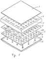
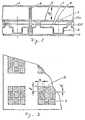
- FIG. 1. 2 The flat antennan array with various polarisations (Fig. 1. 2) contains established with observance of given distance a protective dielectric cover 1, on an inner surface of which an array of reflecting elements 2 is carried out and each of which is carried out (Fig. 3) as group symmetric located conducting (metal) platforms 3 rectangular forms and is located above the appropriate radiating aperture 4 conducting plates 5 (Fig. 1.
- a dielectric sheet 9 stimulating elements 11, located under radiating apertures 4 in a conducting plate 5 and electromagneticly connected with them, and two circuits of a feed reception/transmition signals of various polarisations without crossing conductors are placed.
- the specified circuits of a feed contain elements of feed (as pieces of strip lines 12 and elements 13 division of capacity - T-figurative branches of capacity) and four output of a probe 14, 15, 16, 17 (two interaxes output of a probe 14,15 - for one power supply system and two other interaxes output of a probe 16,17- for other power supply system), located in a plane of cross section of an output waveguide 18 in such a manner that the axes of each pair of output probes (14, 15 and 15, 17) are cross, and the centre of a waveguide 18 is an axis of symmetry for interaxes output probes (14,15 and 16.
- Half of stimulating elements 11 appropriate output for signals of various polarisations is connected to one output probes (for example, 14, 16) appropriate circuits of a feed, and other half of stimulating elements by appropriate output is connected to other output probes (15, 17) pairs of interaxes probes of the appropriate circuits of a feed.
- Stimulating elements 11 and the elements of a feed the power supply system are located symmetric concerning a waveguide 18, placed in a central part of the flat antenna of an array and being a general output, taking place through the bottom cover 19 antenna of an array.
- the free sites of a surface of a dielectric sheet 9 are intended under installation on the appropriate ledges 10a, 10 of a conducting plate 5.
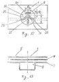
- the stimulating elements 11 are carried out as elements of circular polarisation (in particular, shown on Fig. 5) with output 25, 26 according to the right and left circular polarisation, thus in the antenna on a dielectric sheet 9 (fig. 4), as is stated above, half of stimulating elements by 11 appropriate output 25, 26 for signals of the right and left circular polarisation is connected through elements of a feed of 12, 13 appropriate circuits of a feed, for example, to the appropriate output probes 16, 14 these systems, and other half of stimulating elements 11 output 25, 26 is connected through elements of a feed of 12, 13 appropriate circuits of a feed to other output probes (17, 15) pairs of interaxes probes (14, 15 and 16, 17) appropriate circuits of a feed.
- the pair of interaxes output probes 16, 17 is intended for reception/transmition according to signals of the right circular polarisation
- the pair of interaxes output probes 14, 15 is intended for reception/transmition according to signals of the left circular polarisation
- the zones of cross section of a waveguide 18, located on bisecting-lines between output probes 14,15,16,17 are intended reception/transmition linear polarisations, and other zones of the specified section - reception/transmition elliptic polarisation with elliptical factor from 0 up to 1.
- each reflecting element 2 arrays on an inner surface of a protective dielectric cover 1 is located in the appropriate cell 33 on this surface.
- the whole conducting plate 5 with partitions 31 and ledges 34 can be made from two connected of the top and bottom conducting plates with the appropriate radiating apertures 4, and on the top plate - partitions 31 and ledges 34, and on the bottom plate - ledges 10a for fastening a dielectric sheet 9 are carried out.
- the antenna array works as follows. We shall consider a radiator of a is antennan array in a mode of transmition. At excitation of a pair of interaxes output probes 14, 15 signals through pieces of microstrip lines 12 and the dividers 13 capacity as T-figurative branchings act on the appropriate inputs(entrances) 26 stimulating elements 11. At fulfilment of stimulating elements 11 as elements of circular polarisation (Fig. 5) at a feeding through an input 26 stimulating probes 21, this active probe through a diagonal loop 22 raises a passive probe 20. The additional connection between an active probe 21 and passive probe 20 comes true through a conducting strip 24.
- Length of a diagonal loop 22, conducting strip 24 and distance of a strip from a point of crossing of orthogonal stimulating loops 20, 21 are chosen in such a manner that at a feeding of a stimulating probe 21 (active probe) in a stimulating probe 20 amplitudes of a vector of an electrical field, raised by a probe 21, is approximately equal to amplitude of a vector of an electrical field raised by a probe 20 (passive probe), and the phases of vectors differ on 90. In result a wave of the left circular polarisation is raised.
- each additional reflector is carried out as a symmetric array of reflecting elements that the conditions of passage of each signal of linear polarisation would be identical.
- additional reflectors and in backlashes between their edges is raised electromagnetic fields.
- the field on a radiating surface of each element of a is antennan array - antenna of back radiation, have the square aperture with the party from two up to two with two of two of halves, is close to equal-amplitude and in-phase.
- all stimulating elements of a is antennan array are in-phase in a wide strip of frequencies, field on a surface of a is antennan array in phase and close to equal-amplitude, and operating ratio of a plane of an aperture comes nearer to unit.
- the accepted waves in the return order consecutive raise an electromagnetic field and currents on conducting (metal) platforms 3 and in backlashes between these platforms 3, in stimulating apertures 4, in stimulating orthogonal probes 20 and 21, and then through pieces of microstrip lines 12 and dividers 13 capacity the signals act on a pair of interaxes output probes 14, 15, and on a output probe 14 signals from one half of stimulating elements 11, antenna located on that part act, where this probe 14 is located, and on a output probe 15 - from other half of stimulating elements 11, antenna located on other part, where a probe 15 is located.
- the offered design of the antenna allows to accept signals of various polarisations - linear and elliptic polarisation with factor of an elliptical from 0 up to 1.
- a design of stimulating elements as two mutual - orthogonal probe 20, 21 can be applied, between which on a diagonal a loop galvanically connected to them of 22 lengths (0,35...0,45) and strip of 24 lengths (0,25...0,35) placed on distance no more than 0,2 from a point 23 crossings of mutual - orthogonal probes perpendicularly to a loop 22, for reception of necessary peak and phase distribution is located.
- the converter with one input is used and the entrance probe of the converter is located in a plane, taking place through a longitudinal axes of two output probes of the antenna, a signal of one of two circular polarisations is accepted.
- a signal of one of two circular polarisations is accepted.
- At turn of the converter with one input on 90 around longitudinal axis of a output waveguide 18 antenna is accepted a signal of other circular polarisation. If the converter is located in such a manner that the plane, taking place through an entrance probe of the converter does not pass through output probes 14, 15 and 16, 17 antenna, there is the simultaneous reception on an entrance probe of signals of the right and left circular polarisations with amplitudes, dependent on a situation of an entrance probe of the converter.
- the stimulating element For reception of signals with double linear polarisation the stimulating element is carried out (fig. 7) as two mutual - orthogonal probes 27, 28.
- the stimulating element At excitation of a pair of interaxes output probes 14, 15 signals through pieces of microstrip lines 12 and the dividers 13 capacity act through the appropriate inputs 30 stimulating elements 11 on one (28) from a pair of mutual - orthogonal probes.
- the vector of an electrical field, raised by a probe 28 coincides with a longitudinal axis of this probe.
- the resulting vector of an electrical field, raised (or accepted) flat antenna by an array coincides on a direction with a longitudinal axis of a stimulating probe 28 and the flat antennan array has linear (for example, vertical) polarisation.
- the stimulating probe 27 Passive in the given moment of time the stimulating probe 27 is located to a crossly active stimulating probe 28 and at a feeding of a probe 28 is not raised.
- the signals act on stimulating probes 27 and the flat antennan array has horizontal polarisation.
- Height h of partitions of 31 these cells which are located on perimeter of the basic reflector of each antenna of back radiation, does not exceed thirty five 100-th lengths of a wave, i. e. the walls do not concern to an inner surface of a protective cover 1 and galvanic contact to an additional reflector is not required.
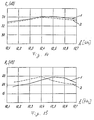
- the flat slot-hole antennan array with various polarisations, carried out according to the invention and used for direct satellite TV, at the sizes of the radiating aperture 456x456 mm and thickness of 26 mm has for circular polarisation in a range of frequencies 12,2...12,7 GHz factor of amplification for the left polarisation no less than 33,1 dB, thus the maximum meaning 34,1 dB, factor of amplification for the right circular polarisation no less than 33,4 dB, and maximum meaning 34,3 dB.
- the sizes has for vertical polarisation factor of amplification no less than 33,2 dB in a strip of frequencies 12,2...12,7 GHz, thus the maximum meaning 34,1 dB, for horizontal polarisation - not less than 33,6 dB in a strip of frequencies, thus the maximum meaning 34,5 dB.
- An outcome on cross-polarisation for vertical and horizontal polarisation no less than 22dB.
Landscapes
- Physics & Mathematics (AREA)
- Electromagnetism (AREA)
- Engineering & Computer Science (AREA)
- Manufacturing & Machinery (AREA)
- Variable-Direction Aerials And Aerial Arrays (AREA)
- Waveguide Aerials (AREA)
Applications Claiming Priority (5)
| Application Number | Priority Date | Filing Date | Title |
|---|---|---|---|
| RU94022013/09A RU2075259C1 (ru) | 1994-06-09 | 1994-06-09 | Плоская антенная решетка с различными поляризациями |
| RU94022012/09A RU2075256C1 (ru) | 1994-06-09 | 1994-06-09 | Микрополосковый излучатель с двойной круговой полимеризацией |
| RU94022012 | 1994-06-09 | ||
| RU94022013 | 1994-06-09 | ||
| PCT/RU1995/000129 WO1995034104A1 (fr) | 1994-06-09 | 1995-06-09 | Antenne reseau plane et element rayonnant a microbandes associe |
Publications (2)
| Publication Number | Publication Date |
|---|---|
| EP0802578A1 true EP0802578A1 (fr) | 1997-10-22 |
| EP0802578A4 EP0802578A4 (fr) | 2000-12-20 |
Family
ID=26653793
Family Applications (1)
| Application Number | Title | Priority Date | Filing Date |
|---|---|---|---|
| EP95924549A Withdrawn EP0802578A4 (fr) | 1994-06-09 | 1995-06-09 | Antenne reseau plane et element rayonnant a microbandes associe |
Country Status (5)
| Country | Link |
|---|---|
| US (1) | US5936579A (fr) |
| EP (1) | EP0802578A4 (fr) |
| KR (1) | KR100270212B1 (fr) |
| AU (1) | AU2899995A (fr) |
| WO (1) | WO1995034104A1 (fr) |
Cited By (2)
| Publication number | Priority date | Publication date | Assignee | Title |
|---|---|---|---|---|
| US7486156B2 (en) | 2005-10-19 | 2009-02-03 | Electronics And Telecommunications Research Institute | Millimeter-wave band broadband microstrip-waveguide transition apparatus having a main patch and a parasitic patch on different dielectric substrates |
| WO2010069350A1 (fr) * | 2008-12-18 | 2010-06-24 | Integrated Electronic Systems !Sys Consulting Gmbh | Antenne plate |
Families Citing this family (21)
| Publication number | Priority date | Publication date | Assignee | Title |
|---|---|---|---|---|
| US6122482A (en) * | 1995-02-22 | 2000-09-19 | Global Communications, Inc. | Satellite broadcast receiving and distribution system |
| DE19742090A1 (de) * | 1997-09-24 | 1999-03-25 | Bosch Gmbh Robert | Ebene Mikrowellenantenne |
| ES2180425B2 (es) * | 2001-04-16 | 2006-08-01 | Universidad Politecnica De Madrid | Agrupamiento de antenas impresas de banda ancha situadas sobre cavidades y excitadas mediante sonda coaxial capacitiva. |
| WO2002103846A1 (fr) * | 2001-06-15 | 2002-12-27 | E-Tenna Corporation | Antenne a ouverture equipee d'un support a faible impedance |
| JP2004015408A (ja) * | 2002-06-06 | 2004-01-15 | Oki Electric Ind Co Ltd | スロットアレーアンテナ |
| US6947003B2 (en) * | 2002-06-06 | 2005-09-20 | Oki Electric Industry Co., Ltd. | Slot array antenna |
| JP4407617B2 (ja) * | 2005-10-20 | 2010-02-03 | 株式会社デンソー | 無線通信システム |
| RU2305879C2 (ru) * | 2005-11-15 | 2007-09-10 | Закрытое Акционерное Общество "Транзас" | Сканирующая антенная решетка |
| JP4572922B2 (ja) * | 2007-10-16 | 2010-11-04 | 株式会社日本自動車部品総合研究所 | アンテナシステムおよび車内用無線通信機 |
| US20100109840A1 (en) * | 2008-10-31 | 2010-05-06 | Robert Schilling | Radio Frequency Identification Read Antenna |
| US8988294B2 (en) | 2011-12-06 | 2015-03-24 | Viasat, Inc. | Antenna with integrated condensation control system |
| US9685707B2 (en) * | 2012-05-30 | 2017-06-20 | Raytheon Company | Active electronically scanned array antenna |
| KR101426055B1 (ko) * | 2013-06-27 | 2014-09-22 | 주식회사 마이크로페이스 | 확장가능한 도파관 안테나 |
| US9876283B2 (en) | 2014-06-19 | 2018-01-23 | Raytheon Company | Active electronically scanned array antenna |
| US9859597B2 (en) | 2015-05-27 | 2018-01-02 | Viasat, Inc. | Partial dielectric loaded septum polarizer |
| US9640847B2 (en) | 2015-05-27 | 2017-05-02 | Viasat, Inc. | Partial dielectric loaded septum polarizer |
| CN105449365B (zh) * | 2015-11-19 | 2019-03-26 | 北京遥测技术研究所 | 一种宽频段双圆极化平板自跟踪天线 |
| CN106207439B (zh) * | 2016-09-08 | 2023-03-24 | 中国电子科技集团公司第五十四研究所 | 一种双圆极化天线单元及阵列天线 |
| US10367259B2 (en) | 2017-01-12 | 2019-07-30 | Arris Enterprises Llc | Antenna with enhanced azimuth gain |
| CN115119424B (zh) * | 2022-06-07 | 2025-09-26 | 深圳市景旺电子股份有限公司 | 相控阵天线pcb及其压合方法 |
| KR20240175425A (ko) * | 2023-06-13 | 2024-12-20 | 현대모비스 주식회사 | 내장 안테나 |
Family Cites Families (17)
| Publication number | Priority date | Publication date | Assignee | Title |
|---|---|---|---|---|
| US3587110A (en) * | 1969-07-01 | 1971-06-22 | Rca Corp | Corporate-network printed antenna system |
| US4291312A (en) * | 1977-09-28 | 1981-09-22 | The United States Of America As Represented By The Secretary Of The Navy | Dual ground plane coplanar fed microstrip antennas |
| US4347517A (en) * | 1981-01-26 | 1982-08-31 | The United States Of America As Represented By The Secretary Of The Navy | Microstrip backfire antenna |
| FR2505097A1 (fr) * | 1981-05-04 | 1982-11-05 | Labo Electronique Physique | Element rayonnant ou recepteur de signaux hyperfrequences a polarisations circulaires et antenne plane hyperfrequence comprenant un reseau de tels elements |
| US4605932A (en) * | 1984-06-06 | 1986-08-12 | The United States Of America As Represented By The Secretary Of The Navy | Nested microstrip arrays |
| FR2592233B1 (fr) * | 1985-12-20 | 1988-02-12 | Radiotechnique Compelec | Antenne plane hyperfrequences recevant simultanement deux polarisations. |
| US4692769A (en) * | 1986-04-14 | 1987-09-08 | The United States Of America As Represented By The Secretary Of The Navy | Dual band slotted microstrip antenna |
| US5005019A (en) * | 1986-11-13 | 1991-04-02 | Communications Satellite Corporation | Electromagnetically coupled printed-circuit antennas having patches or slots capacitively coupled to feedlines |
| US4766440A (en) * | 1986-12-11 | 1988-08-23 | The United States Of America As Represented By The Secretary Of The Navy | Triple frequency U-slot microstrip antenna |
| US4903033A (en) * | 1988-04-01 | 1990-02-20 | Ford Aerospace Corporation | Planar dual polarization antenna |
| US5001492A (en) * | 1988-10-11 | 1991-03-19 | Hughes Aircraft Company | Plural layer co-planar waveguide coupling system for feeding a patch radiator array |
| GB8904302D0 (en) * | 1989-02-24 | 1989-04-12 | Marconi Co Ltd | Microwave antenna array |
| JPH0456502A (ja) * | 1990-06-26 | 1992-02-24 | Matsushita Electric Works Ltd | 平面アンテナ |
| GB2241831B (en) * | 1990-03-07 | 1994-05-25 | Stc Plc | Antenna |
| US5241322A (en) * | 1991-03-21 | 1993-08-31 | Gegan Michael J | Twin element coplanar, U-slot, microstrip antenna |
| GB2261771B (en) * | 1991-11-20 | 1995-08-30 | Northern Telecom Ltd | Flat plate antenna |
| US5661494A (en) * | 1995-03-24 | 1997-08-26 | The United States Of America As Represented By The Administrator Of The National Aeronautics And Space Administration | High performance circularly polarized microstrip antenna |
-
1995
- 1995-06-09 EP EP95924549A patent/EP0802578A4/fr not_active Withdrawn
- 1995-06-09 KR KR1019960707032A patent/KR100270212B1/ko not_active Expired - Fee Related
- 1995-06-09 WO PCT/RU1995/000129 patent/WO1995034104A1/fr not_active Ceased
- 1995-06-09 AU AU28999/95A patent/AU2899995A/en not_active Abandoned
- 1995-06-09 US US08/750,423 patent/US5936579A/en not_active Expired - Fee Related
Cited By (2)
| Publication number | Priority date | Publication date | Assignee | Title |
|---|---|---|---|---|
| US7486156B2 (en) | 2005-10-19 | 2009-02-03 | Electronics And Telecommunications Research Institute | Millimeter-wave band broadband microstrip-waveguide transition apparatus having a main patch and a parasitic patch on different dielectric substrates |
| WO2010069350A1 (fr) * | 2008-12-18 | 2010-06-24 | Integrated Electronic Systems !Sys Consulting Gmbh | Antenne plate |
Also Published As
| Publication number | Publication date |
|---|---|
| US5936579A (en) | 1999-08-10 |
| AU2899995A (en) | 1996-01-04 |
| WO1995034104A1 (fr) | 1995-12-14 |
| KR100270212B1 (ko) | 2000-10-16 |
| EP0802578A4 (fr) | 2000-12-20 |
Similar Documents
| Publication | Publication Date | Title |
|---|---|---|
| EP0802578A1 (fr) | Antenne reseau plane et element rayonnant a microbandes associe | |
| US5262791A (en) | Multi-layer array antenna | |
| US5416492A (en) | Electromagnetic radiator using a leaky NRD waveguide | |
| US4775866A (en) | Two-frequency slotted planar antenna | |
| US5461392A (en) | Transverse probe antenna element embedded in a flared notch array | |
| US5945938A (en) | RF identification transponder | |
| US3995277A (en) | Microstrip antenna | |
| EP0329079B1 (fr) | Antenne guide d'ondes à fentes | |
| EP0456680B1 (fr) | Reseaux d'antennes | |
| US4839663A (en) | Dual polarized slot-dipole radiating element | |
| Suzuki et al. | Circularly polarised radiation from singly fed equilateral-triangular microstrip antenna | |
| US8482472B2 (en) | Planar antenna | |
| JPS6220403A (ja) | スロツト給電アレイアンテナ | |
| US3701162A (en) | Planar antenna array | |
| EP0410083A1 (fr) | Antenne à tente annulaire | |
| US5327148A (en) | Ferrite microstrip antenna | |
| EP0209220B1 (fr) | Dispositif d'alimentation pour une antenne réseau à fentes résonantes alimentée par les deux extrémités | |
| US4507664A (en) | Dielectric image waveguide antenna array | |
| JPS60217702A (ja) | 円偏波円錐ビ−ムアンテナ | |
| US12283756B2 (en) | Antenna array element with dual polarization, antenna array including antenna array element and electronic device including antenna array | |
| US6930647B2 (en) | Semicircular radial antenna | |
| RU2161848C1 (ru) | Плоская антенная решетка и возбуждающий элемент для плоской антенной решетки | |
| Hall et al. | Survey of design techniques for flat profile microwave antennas and arrays | |
| JPH06125214A (ja) | 平面アンテナ | |
| RU2118874C1 (ru) | Вибраторная решетка |
Legal Events
| Date | Code | Title | Description |
|---|---|---|---|
| PUAI | Public reference made under article 153(3) epc to a published international application that has entered the european phase |
Free format text: ORIGINAL CODE: 0009012 |
|
| 17P | Request for examination filed |
Effective date: 19970107 |
|
| AK | Designated contracting states |
Kind code of ref document: A1 Designated state(s): DE FR GB |
|
| RAP1 | Party data changed (applicant data changed or rights of an application transferred) |
Owner name: ZAKRYTOE AKTIONERNOE OBSCHESTVO "FLANT" |
|
| A4 | Supplementary search report drawn up and despatched |
Effective date: 20001106 |
|
| AK | Designated contracting states |
Kind code of ref document: A4 Designated state(s): DE FR GB |
|
| 17Q | First examination report despatched |
Effective date: 20010525 |
|
| STAA | Information on the status of an ep patent application or granted ep patent |
Free format text: STATUS: THE APPLICATION IS DEEMED TO BE WITHDRAWN |
|
| 18D | Application deemed to be withdrawn |
Effective date: 20011231 |