EP0803855A2 - Prozessor zur Umwandlung der Anzahl von Bildelementen eines Videosignals und Anzeigegerät mit Verwendung dieses Prozessors - Google Patents
Prozessor zur Umwandlung der Anzahl von Bildelementen eines Videosignals und Anzeigegerät mit Verwendung dieses Prozessors Download PDFInfo
- Publication number
- EP0803855A2 EP0803855A2 EP97106459A EP97106459A EP0803855A2 EP 0803855 A2 EP0803855 A2 EP 0803855A2 EP 97106459 A EP97106459 A EP 97106459A EP 97106459 A EP97106459 A EP 97106459A EP 0803855 A2 EP0803855 A2 EP 0803855A2
- Authority
- EP
- European Patent Office
- Prior art keywords
- video signal
- circuit
- output
- frequency
- pixels
- Prior art date
- Legal status (The legal status is an assumption and is not a legal conclusion. Google has not performed a legal analysis and makes no representation as to the accuracy of the status listed.)
- Withdrawn
Links
Images


Classifications
-
- G—PHYSICS
- G09—EDUCATION; CRYPTOGRAPHY; DISPLAY; ADVERTISING; SEALS
- G09G—ARRANGEMENTS OR CIRCUITS FOR CONTROL OF INDICATING DEVICES USING STATIC MEANS TO PRESENT VARIABLE INFORMATION
- G09G5/00—Control arrangements or circuits for visual indicators common to cathode-ray tube indicators and other visual indicators
- G09G5/003—Details of a display terminal, the details relating to the control arrangement of the display terminal and to the interfaces thereto
- G09G5/006—Details of the interface to the display terminal
- G09G5/008—Clock recovery
-
- G—PHYSICS
- G06—COMPUTING OR CALCULATING; COUNTING
- G06T—IMAGE DATA PROCESSING OR GENERATION, IN GENERAL
- G06T3/00—Geometric image transformations in the plane of the image
- G06T3/40—Scaling of whole images or parts thereof, e.g. expanding or contracting
- G06T3/4007—Scaling of whole images or parts thereof, e.g. expanding or contracting based on interpolation, e.g. bilinear interpolation
-
- G—PHYSICS
- G09—EDUCATION; CRYPTOGRAPHY; DISPLAY; ADVERTISING; SEALS
- G09G—ARRANGEMENTS OR CIRCUITS FOR CONTROL OF INDICATING DEVICES USING STATIC MEANS TO PRESENT VARIABLE INFORMATION
- G09G3/00—Control arrangements or circuits, of interest only in connection with visual indicators other than cathode-ray tubes
- G09G3/20—Control arrangements or circuits, of interest only in connection with visual indicators other than cathode-ray tubes for presentation of an assembly of a number of characters, e.g. a page, by composing the assembly by combination of individual elements arranged in a matrix no fixed position being assigned to or needed to be assigned to the individual characters or partial characters
-
- G—PHYSICS
- G09—EDUCATION; CRYPTOGRAPHY; DISPLAY; ADVERTISING; SEALS
- G09G—ARRANGEMENTS OR CIRCUITS FOR CONTROL OF INDICATING DEVICES USING STATIC MEANS TO PRESENT VARIABLE INFORMATION
- G09G5/00—Control arrangements or circuits for visual indicators common to cathode-ray tube indicators and other visual indicators
- G09G5/003—Details of a display terminal, the details relating to the control arrangement of the display terminal and to the interfaces thereto
- G09G5/005—Adapting incoming signals to the display format of the display terminal
-
- G—PHYSICS
- G09—EDUCATION; CRYPTOGRAPHY; DISPLAY; ADVERTISING; SEALS
- G09G—ARRANGEMENTS OR CIRCUITS FOR CONTROL OF INDICATING DEVICES USING STATIC MEANS TO PRESENT VARIABLE INFORMATION
- G09G5/00—Control arrangements or circuits for visual indicators common to cathode-ray tube indicators and other visual indicators
- G09G5/18—Timing circuits for raster scan displays
-
- G—PHYSICS
- G09—EDUCATION; CRYPTOGRAPHY; DISPLAY; ADVERTISING; SEALS
- G09G—ARRANGEMENTS OR CIRCUITS FOR CONTROL OF INDICATING DEVICES USING STATIC MEANS TO PRESENT VARIABLE INFORMATION
- G09G2300/00—Aspects of the constitution of display devices
- G09G2300/02—Composition of display devices
- G09G2300/026—Video wall, i.e. juxtaposition of a plurality of screens to create a display screen of bigger dimensions
-
- G—PHYSICS
- G09—EDUCATION; CRYPTOGRAPHY; DISPLAY; ADVERTISING; SEALS
- G09G—ARRANGEMENTS OR CIRCUITS FOR CONTROL OF INDICATING DEVICES USING STATIC MEANS TO PRESENT VARIABLE INFORMATION
- G09G2340/00—Aspects of display data processing
- G09G2340/04—Changes in size, position or resolution of an image
- G09G2340/0407—Resolution change, inclusive of the use of different resolutions for different screen areas
- G09G2340/0414—Vertical resolution change
-
- G—PHYSICS
- G09—EDUCATION; CRYPTOGRAPHY; DISPLAY; ADVERTISING; SEALS
- G09G—ARRANGEMENTS OR CIRCUITS FOR CONTROL OF INDICATING DEVICES USING STATIC MEANS TO PRESENT VARIABLE INFORMATION
- G09G2340/00—Aspects of display data processing
- G09G2340/04—Changes in size, position or resolution of an image
- G09G2340/0407—Resolution change, inclusive of the use of different resolutions for different screen areas
- G09G2340/0421—Horizontal resolution change
-
- G—PHYSICS
- G09—EDUCATION; CRYPTOGRAPHY; DISPLAY; ADVERTISING; SEALS
- G09G—ARRANGEMENTS OR CIRCUITS FOR CONTROL OF INDICATING DEVICES USING STATIC MEANS TO PRESENT VARIABLE INFORMATION
- G09G2340/00—Aspects of display data processing
- G09G2340/04—Changes in size, position or resolution of an image
- G09G2340/0442—Handling or displaying different aspect ratios, or changing the aspect ratio
-
- G—PHYSICS
- G09—EDUCATION; CRYPTOGRAPHY; DISPLAY; ADVERTISING; SEALS
- G09G—ARRANGEMENTS OR CIRCUITS FOR CONTROL OF INDICATING DEVICES USING STATIC MEANS TO PRESENT VARIABLE INFORMATION
- G09G5/00—Control arrangements or circuits for visual indicators common to cathode-ray tube indicators and other visual indicators
- G09G5/003—Details of a display terminal, the details relating to the control arrangement of the display terminal and to the interfaces thereto
- G09G5/006—Details of the interface to the display terminal
Definitions
- the present invention relates to a processor which receives a display video signal from a computer or the like and performs various sorts of processing operations over the signal according to specifications of a display device to display it on the display device.
- a display video signal issued from an engineering workstation, a personal computer or a display terminal of a computer is output as a video signal of dots corresponding to picture elements or pixels on a display screen.
- the digital signal can be subjected to various processing operations including conversion of signal format of field frequency or aspect ratio and such image processing as enlargement/reduction (scaling), screen superposition or geometric transform.
- image processing as enlargement/reduction (scaling), screen superposition or geometric transform.
- Output signals issued from these digital signal processing circuits are supposed to be displayed on a display device of a so-called multi-scanning cathode-ray tube (CRT) type, so that horizontal scanning frequency fh, vertical scanning frequency fv, display line number, etc. will vary depending on the format of the input signals and such signal processing contents as enlargement.
- CTR multi-scanning cathode-ray tube
- display devices of the conventional cathode-ray tube (CRT) type have been replaced by display devices of liquid crystal, plasma, LED, etc.
- These display devices have an advantage over the cathode-ray tube type display device that they can be made dimensionally small in depth and thickness with less occupation space and can have a large display screen.
- These display devices have a problem that a coordinate system for representing respective pixels is fixed and thus cannot be changed. That is, in the display device of the fixed pixel number type, the numbers of horizontal and vertical display pixels (also sometimes referred to as pixel numbers, hereinafter) are fixed so that it is difficult to directly display a signal not conforming to the pixel numbers on the display device without subjecting to any operation. More in detail, it has been difficult to directly display a signal having 480 effective lines or a signal having 1024 horizontal effective pixels and 768 effective lines on a display device having 1280 horizontal pixels and 1024 vertical pixels.
- these pixel number converting operations are required to be carried out at a higher speed as the display device is increased in its resolution.
- the dot clock becomes 100MHz or more.
- parallel processing operation is employed.
- the parallel processing operation is such that input pixels are separated into odd-numbered and even-numbered pixels, subjected to a converting operation to provide a double occupation time, and then are subjected to the parallel processing operation by 2 systems of processing circuits.
- enlarging (reducing) factor or scaling factor
- setting of an enlarging (reducing) factor requires data to be intermittently read out from a memory, but the data reading unit from the memory is limited by the number of parallel processing series (2 pixel units for the odd-numbered and even-numbered pixel series), which involves such a problem that it is impossible to freely set the enlarging (reducing) factor, thus making it difficult to perform the parallel processing operation.
- ECL emitter coupled logic
- the above object is attained by performing arithmetic interpolating operation between vertical lines with use of digital signals and by performing interpolating operation between horizontal dots with use of analog signals based on a low pass filter.
- Equation (1) a relationship of equation (1) which follows should be satisfied among a conversion frequency frck of a digital/analog (D/A) converter circuit, a frequency fck of a clock CK to the display device, and a frequency fho of a horizontal synchronization signal HO to be issued to the display device.
- the dot clock to the display device is arranged to have a substantially constant frequency regardless of the format of the input video signal.
- the above low pass filter are arranged to have such characteristics that a frequency band is limited to 1/2 or less of the frequency fck of the display dot clock CK.
- a weight coefficient when 2 lines of data are to be added together as weighted is generated in accordance with a nonlinear function.
- pixel number conversion can be realized without using a high-speed, large-power-consumption and horizontal pixel interpolating circuit based on digital signals. Further, vertical pixel interpolation can be realized using digital signals without causing any deterioration of image quality.
- signals having various resolutions can be displayed with less cost and power consumption on such a small-size display device of a fixed pixel number type as liquid crystal, plasma or LED.
- the signal processor of the present invention When the signal processor of the present invention is employed, there can be provided a small-sized display device which produces a high quality of image with less power consumption and low costs.
- Fig. 1 is a block diagram of a video signal processor 100 in accordance with an embodiment of the present invention, which includes an input terminal 101 to which a video signal SI is applied from an engineering workstation, personal computer or the like, an input terminal 102 to which a composite synchronization signal HI containing a horizontal synchronization signal of the composite synchronization signal HI or horizontal or vertical synchronization information is applied, an input terminal 103 to which a vertical synchronization signal of the video signal SI is applied, an analog/digital (A/D) converter circuit 104 for converting the video signal SI to digital data, a memory 106 for writing therein the video signal converted to the digital data, a synchronizing separator circuit 105 for separating the synchronization signal contained in the input video signal SI or for waveform-shaping the synchronization signals received from the terminals 102 and 103, a write control circuit 107 for generating a write clock and a write control signal to be sent to the memory on the basis of the synchronization information received from the synchronizing
- a video signal received at the terminal 101 is converted by the A/D converter circuit 104 to digital data and then written in the memory 106.
- a sampling clock for use in the A/D converter circuit 104 is generated by a phase-locked loop (PLL) part in the write control circuit 107 on the basis of the horizontal synchronization signal received from the synchronizing separator circuit 105.
- PLL phase-locked loop
- data in the memory 106 is read out to the line interpolating circuit 108 and then subjected to an interpolating operation of adjacent lines for line number conversion.
- the data subjected to the line number change is converted by the D/A converter circuit 110 to an analog signal, subjected by the low pass filter 111 to removal of unnecessary harmonics components, and then output from the terminal 112 as the output video signal SO.
- the change-over switch 116 selectively switches between an output of the D/A converter circuit 110 and an output of the low pass filter 111 to output it from the terminal 112.
- the change-over switch 116 selects the output signal of the low pass filter 111 to be output from the terminal 112 as the output signal SO.
- the change-over switch 116 selects the output signal of the D/A converter circuit 110 to be output from the terminal 112 as the output signal SO.
- the video signal can be output from the output terminal SO to the display device without being subjected to the band restriction of the low pass filter 111.
- the change-over control of the change-over switch 116 is carried out by a control circuit (not shown) externally provided, in substantially the same manner as the change-over of the pixel number of the input video signal.
- the change-over switch 116 may be provided as necessary and thus in some cases, it can be omitted.
- a dot clock signal necessary for the display device is output from the terminal 115.
- terminals 112, 113, 114 and 115 are connected directly to the display device or connected thereto through such an edit controller as a switcher to display the video signal processed by the signal processing circuit.
- the signal processor of the present invention is connected to the display device which can display a signal of 1280 horizontal display pixel dots, 1664 total horizontal dots (including blanking dots), 1024 display effective lines, a total number 1078 of lines, a horizontal scanning frequency of 64.3KHz, a vertical scanning frequency of 60Hz and a dot clock frequency of 107MHz; so that a signal of 1024 horizontal effective pixels, 768 effective lines and a vertical scanning frequency of 70Hz is converted and displayed.
- the signal processor of the present invention performs converting operations by performing the line number conversion through digital processing operation of the line interpolating circuit 108 and by performing the horizontal pixel interpolation through change of the frequency of the read clock to thereby prolong or shorten a display occupation duration of one pixel.
- the A/D converter circuit 104 performs its sampling operation based on the dot clock whose frequency coincides with the effective pixel number of the input video signal, whereby data of 768 lines each having 1024 pixels is written in the memory 106.
- the image data read out from the memory 106 is sent to the line interpolating circuit 108 where the data is subjected to an interpolating operation to generate 4-line data from 3-line data, whereby the input signal of 768 lines is converted to a display signal of 1024 lines.
- the interpolating operation causes conversion of the input data to the output data of 1024 lines each having 1024 pixels.
- blanking data of fields each having 54 lines with 308 pixels per line is attached to the data under control of the read control circuit 109, whereby the data is output to the display device as the video signal of a total of 1332 of horizontal dots and a total of 1078 of lines.
- the device can regard the video signal received from the signal processor as a signal having a total of 1664 of horizontal dots and 1280 of horizontal effective pixels and can display it thereon.
- the display device can prevent aliasing noise caused by harmonics components therein.
- memory read clock is required to be changed according to the format of the input signal and the pixel number of the display device, but in the present invention, the clock is generated by J/K (J and K being natural numbers) multiplying a stable-frequency signal of a crystal oscillation circuit provided within the read control circuit 109 through the phase-locked loop (PLL), J and K being able to be set by an externally-provided control circuit (not shown).
- the clock CK to be sent to the display device may be generated by the crystal oscillation circuit or the like and the memory read clock may be generated by the PLL.
- any arrangement can be employed, so long as the equation (1) is satisfied among the frequency frck of the memory read clock RCK, the frequency fck of the display dot clock CK to be sent to the display device, and the frequency fho of the horizontal synchronization signal HO to be sent to the display device.
- the memory read clock frequency frck is the same as the conversion frequency of the D/A converter circuit 110.
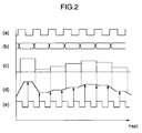
- the waveform of the output of the D/A converter circuit has such consecutive rectangular pulses containing many sharp edges as shown by (c).
- the edge parts in the signal are smoothed through its band limitation, as shown by (d).
- the display dot clock CK (e) having a frequency different from that of the memory read clock in the interior of the display device, a good interpolated output can be obtained without sampling the unstable data of the edge parts.
- the filter When the horizontal effective pixel number of the input video signal is larger than that of the display device, the filter operates as an anti-aliasing filter.
- This low pass filter may made up of such passive elements as inductance, capacitor and resistor.
- the filter may comprise an active filter using a high-speed operational amplifier.
- the filter may comprises an active filter whose cut-off frequency can be externally controlled and whose characteristics can vary with the memory read clock RCK and the display dot clock CK.
- the format of the input video signal is not restricted to the above one, but the pixel number, line number, etc. may be changed as necessary depending on the resister setting by an external control circuit.
- the horizontal and vertical interpolation and scaling factor are changed to convert the format to such a format as to allow the data to be always displayed on the display device.
- the output format of the video signal has been explained in connection with the 1280 x 1024 pixels, the present invention is not limited to the specific example.
- the format of the input video signal may be changed to a signal format suitable for the display device.
- the characteristic of the output stage low pass filter is changed according to the display dot clock CK.
- the characteristic of the low pass filter is previously determined based on the possible highest display dot clock CK, so that when the display pixel number is small, the vertical frequency is increased to make the display dot clock CK equal to the highest display dot clock CK, which results in that the input signal having a plurality of resolutions can be connected to and displayed on the display device with use of a single system of low pass filter.
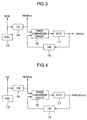
- Shown in Fig. 3 is an arrangement of a clock generator provided in the read control circuit 109.
- the clock generator of Fig. 3 includes an oscillation circuit 13 such as a crystal oscillator for generating the memory read clock RCK, a frequency divider circuit 14 for frequency-dividing the memory read clock RCK by N to generate the horizontal synchronization signal HO, a phase comparison circuit 15 for comparing the phase of an output of a frequency divider circuit 16 with the phase of the horizontal synchronization signal HO, a voltage-controlled oscillator (VCO) 17 whose oscillation frequency is controlled by the phase comparison circuit 15, the frequency divider circuit 16 serving to frequency-divide the display dot clock CK received from the voltage-controlled oscillator (VCO) 17 by M and to input it to the phase comparison circuit 15.
- an oscillation circuit 13 such as a crystal oscillator for generating the memory read clock RCK
- a frequency divider circuit 14 for frequency-dividing the memory read clock RCK by N to generate the horizontal synchronization signal HO
- a phase comparison circuit 15 for comparing the phase of an output of a frequency divider circuit 16 with the phase of the horizontal
- the memory read clock RCK generated by the oscillation circuit 13 is output to the memory 106, D/A converter circuit 110, etc. and is also output to the frequency divider circuit 14 to be frequency-divided thereby to generate the horizontal synchronization signal HO.
- the read control circuit reads data from the memory 106 on a line basis with respect to the horizontal synchronization signal HO as a reference.
- the phase comparison circuit 15, voltage-controlled oscillator (VCO) 17 and frequency divider circuit 16 form such a PLL that the output of the frequency divider circuit 16 applied to the phase comparison circuit 15 is equal to the horizontal synchronization signal HO with respect to frequency, with the result that the PLL operates with the synchronized phase.
- the frequency fck of the dot clock CK corresponds to M times the frequency fho of the output horizontal synchronization signal HO, and the signal HO in turn corresponds to N division of the read frequency frck, whereby a clock satisfying the conditions of the equation (1) can be generated.
- the read clock RCK is generated by the frequency-fixed oscillator and the dot clock CK to be sent to the display device is generated by the PLL in the arrangement of Fig. 3, the dot clock CK to be sent to the display device may be generated by the frequency-fixed oscillator and the read clock RCK may be generated by the PLL, an example of which is shown in Fig. 4.
- Fig. 4 is arranged so that the oscillation circuit 13 generates the display dot clock CK and the frequency divider circuit 16 frequency-divides the clock CK by M to generate the horizontal synchronization signal HO.
- VCO voltage-controlled oscillator
- the frequency frck of the read clock RCK is changed to a frequency corresponding to N times the frequency fho of the horizontal synchronization signal HO.
- a clock satisfying the conditions of the equation (1) can be generated.
- the display dot clock CK is set by an oscillation circuit such as a crystal oscillator to have always a constant frequency, so that, even when the format of the output video signal is changed, it is only required to change the vertical frequency and is unnecessary to change the characteristic of the low pass filter such as cut-off frequency in the foregoing arrangement example, whereby various formats of images can be displayed with use of a single system of filter.
- it is necessary to change the read clock RCK according to the format of the output video signal which can be realized by changing a frequency division ratio N of the frequency divider circuit 14 in Fig. 4, while the frequency of the read clock RCK satisfies the conditions of the equation (1).
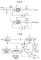
- the circuit of Fig. 5 includes a frequency divider circuit 18 for frequency-dividing a write clock WCK or another fixed clock signal to generate the horizontal synchronization signal HO, phase comparison circuits 15-1 and 15-2, voltage-controlled oscillators (VCOs) 17-1 and 17-2, and frequency divider circuits 14 and 16 having frequency division ratios of N and M respectively.
- VCOs voltage-controlled oscillators
- N and M frequency division ratios of N and M respectively.
- the setting of the frequency division ratio of the frequency divider circuit, the oscillation frequency range of the voltage-controlled oscillator, etc. can be changed, that is, the setting change can be made by an externally-provided control circuit depending on the format of the input video signal or the contents of the signal processing.
- the line interpolation circuit may comprise a conventional linear interpolation circuit but preferably comprise a line interpolation circuit using a nonlinear circuit to be explained below.
- FIG. 6 there is shown a block diagram of an embodiment of a vertical line interpolation circuit in the present embodiment, which includes a buffer memory 1 for storing therein digitized input pixel data, a one-line delay circuit 2 for delaying a signal S1 read out from the buffer memory 1 and outputting it as a signal SO, an interpolation control circuit 3 for performing control over interpolation by setting an enlarging factor, a nonlinear circuit 4 for converting a weight coefficient received from the interpolation control circuit 3 to a nonlinear weight coefficient k according to a nonlinear function, a coefficient weighting circuit 5 for obtaining a weighted average of the signals S1 and S0 with the nonlinear weight coefficients k and 1-k received from the nonlinear circuit 4, a coefficient circuit 501 for multiplying the input S1 by the nonlinear weight coefficient k received from the nonlinear circuit 4, a coefficient circuit 502 for multiplying the input S0 by the nonlinear weight coefficient 1-k, and an addition circuit 503 for
- An input video signal is stored in the buffer memory 1 as digital data.
- the buffer memory functions to accommodate a difference between data transmission rates caused by the pixel number conversion.
- the data S1 read out from the buffer memory is input to the one-line delay circuit 2 comprising a line memory or the like to allow simultaneous reference of the current target pixel data S0 and the pixel data S1 appearing one line later.
- the pixels of the data S0 and S1 are subjected by the coefficient weighting circuit 5 to the coefficient weighting operation with use of the nonlinear weight coefficient k received from the nonlinear circuit 4 to be output therefrom as the interpolated signal Ao which is expressed as follows.
- Ao S1 ⁇ k + S0 ⁇ (1-k) where, 0 ⁇ k ⁇ 1.
- the nonlinear characteristic of the nonlinear circuit 4 causes conversion to the nonlinear weight coefficient k in the present invention, as follows.
- the characteristic k is as follows.
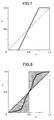
- Fig. 7 is an input/output characteristic diagram showing a relationship of the value of an output k to an input ⁇ of the nonlinear circuit 4.
- the nonlinear circuit 4 can be easily implemented by preparing a look-up table with use of a read-only memory (ROM). That is, the input ⁇ is regarded as a ROM address and the value of the corresponding output k is previously written in the ROM as data.
- ROM read-only memory
- the characteristic of the interpolated output image becomes close to the characteristic of the nearest interpolation (previous-value hold interpolation) to thereby suppress reduction in the resolution of the edge parts.
- the equation (8) shows a condition, when a distance to the interpolation pixel is small, required to make the weight coefficient smaller than that in the linear interpolation system to thereby suppress the resolution deterioration caused by the averaging operation.
- Another example of the nonlinear function satisfying the conditions of the equations (9), (8) and (7) is shown in Fig. 8.
- Any nonlinear function may be employed in the present invention, so long as it meets these conditions, which conforms to the subject matter of the present invention.
- the circuit of Fig. 9 includes a register 301 for setting data for control of an enlarging factor, an addition circuit 302 for adding together a set value of the setting register 301 and an output of a D flip-flop array circuit 303 acting to latch an output of the addition circuit 302 with the horizontal synchronization pulse signal HO, and a coefficient calculation circuit 304 for calculating the weight coefficient based on a interpolation distance DIS received from the D flip-flop array circuit 303.
- the setting register 301, addition circuit 302 and D flip-flop array circuit 303 are of an 8 bit type.
- the cumulative addition output DIS indicates a distance between the interpolation line S0 and interpolation line, e.g., 0, 192, 128, 64,..., the coefficient calculation circuit 304 generates the weight coefficient on the basis of the received signal DIS.
- a line update signal HINC generated from the carry signal causes data to be updated on a line basis from the buffer, thus updating the S0 and S1.
- the new S0 and S1 as well as lower 8 bits of the cumulative addition output can be used to generate an interpolation line.
- Figs. 11A, 11B, 11C and 11D are examples of an input/output characteristic of the coefficient calculation circuit showing a relationship of the output interpolation coefficient to the input value DIS.
- Fig. 11A shows the operation of the coefficient calculation circuit when arranged so that the coefficient linearly varies from 0 to 1.0 as the DIS is increased from 0 to 255.
- a video signal is, in many cases, represented by about 8 bits (R, G, B or Y, R-Y, B-Y respectively independently). For this reason, after subjected to an interpolating operation, the video signal is rounded eventually to about 8 bits, so that, even when interpolation coefficient is controlled in relatively rough steps, this has a less effect on image.
- the input/output characteristic of the coefficient calculation circuit 304 when the interpolation coefficient is controlled in 8 steps is shown in Fig. 11B.
- the number of steps is not limited to the specific 8, but it may be arbitrarily set.
- the step number is set at the power of 2, however, the structure of the coefficient circuit can be simplified with a combination of bit shift and adder.
- ⁇ 0 in the DIS range of 0 to 63
- the present invention is not restricted to the specific example.
- ⁇ may be 0 in the vicinity of the value of the DIS of 0, ⁇ may be 1 in the vicinity of the value of the DIS of 255, and may linearly vary in the vicinity of an intermediate value of the DIS.
- the enlarging operation of (256/N) times can be carried out based on the numeral value N set in the setting register 301.
- the setting register 301, addition circuit 302 and D flip-flop array circuit 303 have been of an 8 bit type in the arrangement of Fig. 6, the present invention is not limited to the specific example.
- the arrangement of Fig. 6 may be of a 7 or 10 bit type.
- the circuit scale can be reduced.
- an increase in the number of bits enables the enlarging factor to be set on a finer unit basis.
- Fig. 12 Shown in Fig. 12 is another embodiment of the interpolation control circuit 3.
- FIG. 12 An arrangement of Fig. 12 corresponds to the coefficient weighting circuit 5 in Fig. 6 but which interior structure is modified. Other arrangement is substantially the same as that in Fig. 6. Explanation will be made as to the interior structure of the coefficient weighting circuit 5.
- the arrangement of the coefficient weighting circuit 5 in Fig. 12 is based on the equation (10).
- a signal (S1-S0) is calculated by a subtraction circuit 504, multiplied by a coefficient circuit 501 by the coefficient k, and then added by an addition circuit 503 to the signal S0 to be thereby output as the interpolated output signal Ao. That is, since the equation (1) is equivalent to the equation (10), even use of the coefficient weighting circuit 5 shown in Fig. 12 can produce effects similar to in the embodiment of Fig. 6.
- a coefficient circuit for performing multiplying operation is, generally speaking, larger in scale than a subtraction circuit, so that, when the circuit is implemented with the arrangement of Fig. 12, the circuit scale can be made small in size.
- the present invention can be applied also to the conversion of the number of horizontal pixels.
- the one-line delay circuit 2 in Fig. 6 or 12 is replaced by a sample delay circuit to obtain an interpolated pixel output with use of data between adjacent pixels.
- the interpolation control circuit 3 of Fig. 9 is arranged so that the horizontal synchronization pulse HO is replaced by the dot clock DCK and the line update signal HINC is replaced by the read clock RCK of the buffer memory 1.
- reference numeral 12 denotes an example of circuit for performing the 2-dimensional pixel interpolating operation in accordance with the present invention.
- the circuit 12 includes a buffer memory 1 for storing therein digitized input pixel data, a line memory 6 for delaying a signal L1 read out from the buffer memory by one line and outputting it, a vertical interpolation control circuit 3a for performing control based on setting of a vertical enlarging factor, a nonlinear circuit 4a for transforming a weight coefficient ⁇ 1 received from the vertical interpolation control circuit 3a into a nonlinear weight coefficient k1 in accordance with a nonlinear function, a coefficient weighting circuit 5a for performing weighted average of the signals L1 and L0 with use of the nonlinear weight coefficients k1 and (1-k1) received from the nonlinear circuit 4a, a one-sample delay circuit 2 for delaying by one sample the signal S1 received from the coefficient weighting circuit 5a and outputting it as an output signal S0, a buffer memory
- a vertical interpolating circuit made up of the line memory 6, coefficient weighting circuit 5a, nonlinear circuit 4a and vertical interpolation control circuit 3a is connected in cascade with a horizontal interpolating circuit made up of the one-sample delay circuit 2, coefficient weighting circuit 5b, nonlinear circuit 4b and horizontal interpolation control circuit 3b.
- the buffer memory 1 functions to accommodate a difference in data transmission rate caused by the conversion of the numbers of horizontal and vertical pixels and the conversion of the number of lines, and is commonly used as both vertical and horizontal interpolation buffers.
- the data L1 issued from the buffer memory 1 is one-line delayed by the line memory 6 and then output therefrom as the signal L0.
- the signals L0 and L1 become vertically adjacent pixels and, when the signals are subjected to the weighting averaging operation with use of the nonlinear weight coefficient k1 received from the nonlinear circuit 4a, vertically interpolated data corresponding to one line can be obtained. This is different from the horizontally interpolating operation used so far, that is, the weight coefficient ⁇ 1 and nonlinear weight coefficient k1 are held during one line and updated whenever the line is changed.
- a control signal RCK1 issued from the vertical interpolation control circuit 3a is for controlling the data update on a line basis. When this signal is not issued, the data of the identical line is repetitively output.
- the data update of the buffer memory 1 and line memory 6 on a sample basis is controlled by a control signal RCK2 issued from the horizontal interpolation control circuit 3b.
- the output signal S1 of the coefficient weighting circuit 5a after subjected to the vertical interpolating operation is one-sample delayed by the one-sample delay circuit 2 so that the pixels S0 and S1 horizontally adjacent on the display screen can be simultaneously referred to.
- the 2 adjacent pixels are subjected by the coefficient weighting circuit 5b to a horizontal interpolating operation with use of the nonlinear weight coefficient k2 received from the nonlinear circuit 4b and then output as an interpolated signal.
- the characteristics of the nonlinear circuits 4a and 4b are set as shown in Fig. 7, as in the embodiments of Figs. 6 and 12.
- the 2-dimensional operations including the enlargement of the entire display screen and the conversion of aspect ratio can be realized with less resolution deterioration and high image quality while suppressing distortion in graphics and character fonts.
- the horizontal nonlinear characteristic may be different from the vertical one.
- video signals of raster scans are made vertically discrete by scanning lines and tend to be susceptible to deterioration even when the vertical interpolation characteristic is close to the nearest (previous-value hold) interpolation characteristic.
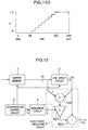
- the line interpolating circuit 108 in Fig. 1 has such an arrangement as shown in Fig. 13 and the low pass filter 111 and change-over switch 116 are not provided.
- Other constituent elements are the same as those in Fig. 1.
- a video signal input from the terminal 101 is converted by the A/D converter circuit 104 to digital data and then written in the memory 106.
- a sampling clock used in the A/D converter circuit 104 is generated by a phase-locked loop (PLL) in the write control circuit 107 on the basis of a horizontal synchronization signal received from the synchronizing separator circuit 105, and the effective zone of the video signal is written in the memory 106.
- PLL phase-locked loop
- the read control circuit 109 which incorporates an oscillation circuit such as a crystal oscillator for outputting a stable frequency, generates a horizontal synchronization signal HO, a vertical synchronization signal VO and a clock CK for display of the video signal on a display device of a fixed pixel number type.
- the data within the memory 106 is converted by the pixel interpolating circuit 12 with respect to the numbers of lines and pixels, converted by the D/A converter circuit 110 to an analog signal, and then output from the terminal 112 as an output video signal SO.
- the read control circuit 109 outputs, in addition to the horizontal synchronization signal HO and vertical synchronization signal VO, a clock CK for the display device requiring the dot clock, the clock CK being output from the terminal 115.
- a display signal of 1024 pixels x 768 lines can be displayed as enlarged fully on the screen of a display device of a fixed pixel number type of 1280 pixels x 1024 lines such as a liquid crystal display.
- the memory 106 writes therein the effective zone of the input signal on a field basis and converts it with respect to field frequency.
- the memory 106 may be commonly used also as the buffer memory 1 in the pixel interpolating circuit 12 of Fig. 13.
- the reading operation from the memory 106 on a line basis is carried out according to the signal RCK1 received from the vertical interpolation control circuit 3a within the pixel interpolating circuit 12 of Fig. 13, while the reading operation on a dot basis is carried out according to the signal RCK2 received from the horizontal interpolation control circuit 3b.
- the common use of the memory enables reduction of the circuit scale.
- the pixels can be number-converted and displayed without remarked deterioration of image quality.
- the order of the memory 106 and the pixel interpolating circuit 12 in Fig. 14 may be reversed as necessary.
- the respective control circuits may control their addresses to the memory or make the read clock frequency different from the write clock frequency in the course of writing and reading these data, thus realizing various image processings including scaling of image size.
- the circuit of Fig. 15 comprises 3 R, G and B systems each of which includes the video signal input terminal 101, A/D converter circuit 104, memory 106, line interpolating circuit 108, D/A converter circuit 110, low pass filter 111 and video signal output terminal 112 in Fig. 1.
- the change-over switch 116 is omitted herein.
- A/D converter circuits 104R, 104B, 104G, memories 106R, 106B, 106G, line interpolating circuits 108R, 108B, 108G, and D/A converter circuits 110R, 110B, 110G are controlled by the write control circuit 107 and read control circuit 109 common to the R, G and B systems.
- Applied to the synchronizing separator circuit 105 is, in addition to synchronization input signals HI and VI independently of the video signal, a G input signal GI from a terminal 101G to cope with the synchronization signal multiplexed with a G signal.
- Other arrangement is substantially the same as that of Fig. 1. With such an arrangement as mentioned above, even color video signal including 3 signals of the R, G and B systems can be processed in substantially the same manner as in the foregoing embodiments.
- change-over switches 116R, 116G and 116B are provided for bypassing the low pass filters 111R, 111G and 111B.
- Shown in Fig. 16 is another embodiment of the video signal processor 100.
- Fig. 16 The arrangement of Fig. 16 is different from that of Fig. 1 in that the order of the memory 106 and line interpolating circuit 108 is reversed.
- digital data issued from the A/D converter circuit 104 is subjected by the line interpolating circuit 108 to a line number conversion and then written in the memory 106. Since the line number conversion is carried out at the stage of writing it in the memory, the line interpolating circuit 108 is controlled by the write control circuit 107. Since the data written in the memory 106 is already subjected to the line number conversion, when it is desired to read the data from the memory 106, it is only required to convert the clock frequency to conform to the horizontal pixel number of a display device. With such an arrangement, when the number of effective lines of an input video signal is larger than that of the display device, the necessary capacity of the memory 106 can be made small. That is, at this time, the memory 106 performs vertical band limiting and line decimating operations.
- the signal processor of the present invention has been provided independently of the display device. Explanation will next be made as to an embodiment in which the signal processor of the present invention is built in a display device, with reference to Fig. 17.
- reference numeral 100 denotes a signal processor of the present invention
- numeral 10 denotes a display device
- 9 denotes a display device of a fixed display pixel number type such as a liquid crystal display or a plasma display
- 7 denotes a signal processing circuit for converting to signals necessary for the display apparatus
- 8 denotes a synchronization processing circuit for horizontal and vertical scan.
- Video signals RO, BO and GO processed by the signal processor 100 of the present invention are subjected by the signal processing circuit 7 to conversion of voltages or currents necessary to operate the display device 9.
- a horizontal synchronization signal HO, a vertical synchronization signal VO and dot clock CK issued from the signal processor 100 are applied to the synchronization processing circuit 8 to be processed to cause horizontal and vertical scan of the display device 9. More specifically, in the liquid crystal or plasma display device, driver operations are performed to determine X and Y coordinates.
- incorporation of the signal processor within the display apparatus can advantageously economically eliminate the need for provision of an independent power supply and casing.
- the signal processor of the present invention performs its operation in a 1:1 relationship to the display apparatus, so that the incorporation of the signal processor in the display apparatus enables the suppression of increase in the number of wiring lines, thus realizing a display device having a high level of function.
Landscapes
- Engineering & Computer Science (AREA)
- General Physics & Mathematics (AREA)
- Theoretical Computer Science (AREA)
- Physics & Mathematics (AREA)
- Computer Hardware Design (AREA)
- Multimedia (AREA)
- Control Of Indicators Other Than Cathode Ray Tubes (AREA)
- Controls And Circuits For Display Device (AREA)
- Image Processing (AREA)
- Facsimile Image Signal Circuits (AREA)
- Transforming Electric Information Into Light Information (AREA)
- Liquid Crystal Display Device Control (AREA)
- Editing Of Facsimile Originals (AREA)
Applications Claiming Priority (8)
| Application Number | Priority Date | Filing Date | Title |
|---|---|---|---|
| JP100883/96 | 1996-04-23 | ||
| JP10088396 | 1996-04-23 | ||
| JP10088396 | 1996-04-23 | ||
| JP19433796 | 1996-07-24 | ||
| JP8194337A JPH1011009A (ja) | 1996-04-23 | 1996-07-24 | 映像信号の処理装置及びこれを用いた表示装置 |
| JP194337/96 | 1996-07-24 | ||
| WOPCT/JP96/02468 | 1996-09-02 | ||
| PCT/JP1996/002468 WO1998010377A1 (en) | 1996-04-23 | 1996-09-02 | Video signal processor |
Publications (2)
| Publication Number | Publication Date |
|---|---|
| EP0803855A2 true EP0803855A2 (de) | 1997-10-29 |
| EP0803855A3 EP0803855A3 (de) | 1999-06-16 |
Family
ID=27307987
Family Applications (1)
| Application Number | Title | Priority Date | Filing Date |
|---|---|---|---|
| EP97106459A Withdrawn EP0803855A3 (de) | 1996-04-23 | 1997-04-18 | Prozessor zur Umwandlung der Anzahl von Bildelementen eines Videosignals und Anzeigegerät mit Verwendung dieses Prozessors |
Country Status (4)
| Country | Link |
|---|---|
| US (1) | US5986635A (de) |
| EP (1) | EP0803855A3 (de) |
| JP (1) | JPH1011009A (de) |
| WO (1) | WO1998010377A1 (de) |
Cited By (3)
| Publication number | Priority date | Publication date | Assignee | Title |
|---|---|---|---|---|
| WO2006073792A1 (en) * | 2004-12-31 | 2006-07-13 | Thomson Licensing | Multi-standard vertical scan crt display |
| CN1301001C (zh) * | 2003-09-17 | 2007-02-14 | 诺日士钢机株式会社 | 图像处理装置及方法 |
| US7652652B2 (en) | 2002-11-12 | 2010-01-26 | Sharp Kabushiki Kaisha | Data signal line driving method, data signal line driving circuit, and display device using the same |
Families Citing this family (25)
| Publication number | Priority date | Publication date | Assignee | Title |
|---|---|---|---|---|
| DE19737326A1 (de) * | 1997-08-27 | 1999-03-04 | Thomson Brandt Gmbh | Verfahren zur Gewinnung von Zeilensynchronisationsinformationen aus einem Videosignal und Vorrichtung zur Durchführung des Verfahrens |
| TW377429B (en) * | 1998-02-11 | 1999-12-21 | Au Optronics Corp | Method of showing graphics on dot matrix display |
| JP4224876B2 (ja) * | 1998-09-11 | 2009-02-18 | ソニー株式会社 | 記憶装置、並びに書き込み方法および読み出し方法 |
| US6232952B1 (en) * | 1998-09-30 | 2001-05-15 | Genesis Microchip Corp. | Method and apparatus for comparing frequently the phase of a target clock signal with the phase of a reference clock signal enabling quick synchronization |
| US6480632B2 (en) * | 1998-12-03 | 2002-11-12 | Intel Corporation | Method and apparatus to interpolate video frames |
| JP2000305555A (ja) * | 1999-04-19 | 2000-11-02 | Sony Corp | 画像表示装置 |
| JP2001134753A (ja) * | 1999-11-08 | 2001-05-18 | Sony Corp | 補間処理装置、補間処理方法及び画像表示装置 |
| US6369787B1 (en) * | 2000-01-27 | 2002-04-09 | Myson Technology, Inc. | Method and apparatus for interpolating a digital image |
| US6577778B1 (en) * | 2000-01-27 | 2003-06-10 | Myson Century, Inc. | Method and apparatus for interpolating a digital image |
| US6742008B2 (en) * | 2001-03-01 | 2004-05-25 | Micron Technology, Inc. | Accurate and cost effective linear interpolators |
| JP4827213B2 (ja) * | 2001-03-12 | 2011-11-30 | 株式会社メガチップス | 画像補正装置および画像補正方法 |
| JP2003069959A (ja) * | 2001-06-14 | 2003-03-07 | Sony Corp | 映像信号処理回路、映像信号処理方法、および画像表示装置 |
| US7483080B2 (en) * | 2003-10-31 | 2009-01-27 | Ati Technologies Ulc | System for displaying images and method thereof |
| US6995526B1 (en) * | 2004-08-09 | 2006-02-07 | National Semiconductor Corporation | Digitally controlled vertical C linearity correction with constant start and end points without using an AGC |
| US7355652B2 (en) * | 2004-10-13 | 2008-04-08 | Cirrus Logic, Inc. | Inverse tracking over two different clock domains |
| JP2006243641A (ja) * | 2005-03-07 | 2006-09-14 | Matsushita Electric Ind Co Ltd | 映像表示制御装置及び映像表示装置 |
| JP4761806B2 (ja) * | 2005-03-31 | 2011-08-31 | 株式会社東芝 | 画像データ処理装置 |
| TWI271104B (en) * | 2005-09-19 | 2007-01-11 | Novatek Microelectronics Corp | Device and method for zooming images |
| JP5288579B2 (ja) * | 2006-12-13 | 2013-09-11 | ルネサスエレクトロニクス株式会社 | 表示装置及び、コントローラドライバ |
| JP4932644B2 (ja) * | 2007-08-30 | 2012-05-16 | オンセミコンダクター・トレーディング・リミテッド | 画像データ処理装置 |
| WO2010091750A1 (en) * | 2009-02-12 | 2010-08-19 | Zoran (France) | Scaling method and device for image signals |
| US8223057B2 (en) * | 2010-09-30 | 2012-07-17 | Schneider Electric USA, Inc. | Quantizing sampled inputs using fixed frequency analog to digital conversions through interpolation |
| CN105118458B (zh) * | 2015-09-15 | 2018-06-29 | 深圳市华星光电技术有限公司 | 驱动装置以及液晶显示器 |
| US9813659B1 (en) | 2016-05-11 | 2017-11-07 | Drone Racing League, Inc. | Diversity receiver |
| US10737781B2 (en) | 2017-09-14 | 2020-08-11 | Drone Racing League, Inc. | Three-dimensional pathway tracking system |
Family Cites Families (16)
| Publication number | Priority date | Publication date | Assignee | Title |
|---|---|---|---|---|
| JPS6033791A (ja) * | 1983-08-04 | 1985-02-21 | Toshiba Corp | ディジタルコンバ−ジェンス補正装置 |
| GB2224410A (en) * | 1988-10-26 | 1990-05-02 | Marconi Gec Ltd | Video image magnification system |
| US5054100A (en) * | 1989-11-16 | 1991-10-01 | Eastman Kodak Company | Pixel interpolator with edge sharpening |
| US5422678A (en) * | 1991-01-29 | 1995-06-06 | Seiko Epson Corp. | Video processor for enlarging and contracting an image in a vertical direction |
| JP2502829B2 (ja) * | 1991-03-22 | 1996-05-29 | 松下電器産業株式会社 | 画像表示装置 |
| US5229853A (en) * | 1991-08-19 | 1993-07-20 | Hewlett-Packard Company | System for converting a video signal from a first format to a second format |
| JP3034659B2 (ja) * | 1991-09-26 | 2000-04-17 | 株式会社日立製作所 | 拡大画面表示回路及びそれに用いられる水平フィルタ回路 |
| JPH05158464A (ja) * | 1991-12-09 | 1993-06-25 | Toshiba Corp | 解像度変換回路 |
| JPH05284334A (ja) * | 1992-04-01 | 1993-10-29 | Ricoh Co Ltd | 非線形補間装置 |
| JP3143209B2 (ja) * | 1992-05-25 | 2001-03-07 | 株式会社リコー | 画像変倍装置 |
| US5585864A (en) * | 1992-06-24 | 1996-12-17 | Seiko Epson Corporation | Apparatus for effecting high speed transfer of video data into a video memory using direct memory access |
| JPH06177706A (ja) * | 1992-12-08 | 1994-06-24 | Sony Corp | 信号処理装置 |
| US5457457A (en) * | 1993-12-07 | 1995-10-10 | Nippon Columbia Co., Ltd. | Digital to analog conversion device which decreases low level high frequency noise |
| JP3307750B2 (ja) * | 1993-12-28 | 2002-07-24 | キヤノン株式会社 | 表示制御装置 |
| US5541666A (en) * | 1994-07-06 | 1996-07-30 | General Instrument | Method and apparatus for overlaying digitally generated graphics over an analog video signal |
| US5801678A (en) * | 1996-04-26 | 1998-09-01 | Industrial Technology Research Institute | Fast bi-linear interpolation pipeline |
-
1996
- 1996-07-24 JP JP8194337A patent/JPH1011009A/ja active Pending
- 1996-09-02 WO PCT/JP1996/002468 patent/WO1998010377A1/ja not_active Ceased
-
1997
- 1997-04-18 EP EP97106459A patent/EP0803855A3/de not_active Withdrawn
- 1997-04-22 US US08/837,747 patent/US5986635A/en not_active Expired - Lifetime
Cited By (3)
| Publication number | Priority date | Publication date | Assignee | Title |
|---|---|---|---|---|
| US7652652B2 (en) | 2002-11-12 | 2010-01-26 | Sharp Kabushiki Kaisha | Data signal line driving method, data signal line driving circuit, and display device using the same |
| CN1301001C (zh) * | 2003-09-17 | 2007-02-14 | 诺日士钢机株式会社 | 图像处理装置及方法 |
| WO2006073792A1 (en) * | 2004-12-31 | 2006-07-13 | Thomson Licensing | Multi-standard vertical scan crt display |
Also Published As
| Publication number | Publication date |
|---|---|
| JPH1011009A (ja) | 1998-01-16 |
| EP0803855A3 (de) | 1999-06-16 |
| WO1998010377A1 (en) | 1998-03-12 |
| US5986635A (en) | 1999-11-16 |
Similar Documents
| Publication | Publication Date | Title |
|---|---|---|
| US5986635A (en) | Processor for converting pixel number of video signal and display apparatus using the same | |
| US5528301A (en) | Universal video format sample size converter | |
| US5914753A (en) | Apparatus and method to convert computer graphics signals to television video signals with vertical and horizontal scaling requiring no frame buffers | |
| US6466272B1 (en) | Display apparatus | |
| KR910005363B1 (ko) | 저 분해능 비디오 신호를 고 분해능 비디오 모니터상에 표시하기 위한 비디오 장치 및 그 방법 | |
| JP3228420B2 (ja) | 非対称画面圧縮 | |
| EP1164568B1 (de) | Videosignal konvertierungsvorrichtung und videosignal konvertierungsverfahren | |
| US7136110B2 (en) | Image signal processing apparatus | |
| EP0653742A2 (de) | Vorrichtung zur Echtzeitskalierung von Bildern in einem Multimedien Arbeitsplatz | |
| JPH05241524A (ja) | ユニバーサルビデオ出力装置 | |
| US6107984A (en) | Processor of video signal and display unit using the same | |
| JP2003015617A (ja) | 映像信号処理方法及び装置 | |
| CA1230669A (en) | Progressive scan television display system | |
| JPH06205327A (ja) | インターレース型及びノンインターレース型ビデオ信号表示装置 | |
| US6040868A (en) | Device and method of converting scanning pattern of display device | |
| JPH07199855A (ja) | ドットマトリクス型表示装置 | |
| JPS63181572A (ja) | ス−パ−インポ−ズ装置 | |
| JP3405208B2 (ja) | 分割マルチ画面表示装置 | |
| US5177609A (en) | Video signal time base compression apparatus | |
| JP3484763B2 (ja) | 映像データ転送装置およびコンピュータシステム | |
| KR100743520B1 (ko) | 비디오 스케일러 및 스케일링 방법 | |
| JPH07123335A (ja) | 2画面表示テレビジョン受像機 | |
| JP3894173B2 (ja) | 映像データ転送を行うコンピュータシステム | |
| KR0123769B1 (ko) | 16 : 9 화면에서의 픽쳐 인 픽쳐 표시회로 | |
| JPH07261691A (ja) | ディスプレイ装置 |
Legal Events
| Date | Code | Title | Description |
|---|---|---|---|
| PUAI | Public reference made under article 153(3) epc to a published international application that has entered the european phase |
Free format text: ORIGINAL CODE: 0009012 |
|
| 17P | Request for examination filed |
Effective date: 19970418 |
|
| AK | Designated contracting states |
Kind code of ref document: A2 Designated state(s): DE FR GB |
|
| PUAL | Search report despatched |
Free format text: ORIGINAL CODE: 0009013 |
|
| AK | Designated contracting states |
Kind code of ref document: A3 Designated state(s): DE FR GB |
|
| RIC1 | Information provided on ipc code assigned before grant |
Free format text: 6G 09G 3/20 A, 6H 04N 7/01 B |
|
| 17Q | First examination report despatched |
Effective date: 20000203 |
|
| STAA | Information on the status of an ep patent application or granted ep patent |
Free format text: STATUS: THE APPLICATION IS DEEMED TO BE WITHDRAWN |
|
| 18D | Application deemed to be withdrawn |
Effective date: 20010424 |