EP0804062A2 - Unité d'un dispositif électronique - Google Patents
Unité d'un dispositif électronique Download PDFInfo
- Publication number
- EP0804062A2 EP0804062A2 EP96120889A EP96120889A EP0804062A2 EP 0804062 A2 EP0804062 A2 EP 0804062A2 EP 96120889 A EP96120889 A EP 96120889A EP 96120889 A EP96120889 A EP 96120889A EP 0804062 A2 EP0804062 A2 EP 0804062A2
- Authority
- EP
- European Patent Office
- Prior art keywords
- eject
- electronic device
- case
- device unit
- card
- Prior art date
- Legal status (The legal status is an assumption and is not a legal conclusion. Google has not performed a legal analysis and makes no representation as to the accuracy of the status listed.)
- Withdrawn
Links
- 239000004020 conductor Substances 0.000 claims abstract description 4
- 230000007246 mechanism Effects 0.000 claims description 13
- 238000005452 bending Methods 0.000 claims description 7
- 238000000034 method Methods 0.000 abstract description 6
- 238000004519 manufacturing process Methods 0.000 abstract description 5
- 238000004891 communication Methods 0.000 description 9
- 238000003780 insertion Methods 0.000 description 9
- 230000037431 insertion Effects 0.000 description 9
- 238000005476 soldering Methods 0.000 description 6
- 239000002184 metal Substances 0.000 description 3
- QXOQNNAWFUXKMH-UHFFFAOYSA-N 1-(Malonylamino)cyclopropanecarboxylic acid Chemical compound OC(=O)CC(=O)NC1(C(O)=O)CC1 QXOQNNAWFUXKMH-UHFFFAOYSA-N 0.000 description 2
- 238000010586 diagram Methods 0.000 description 2
- 241001123862 Mico Species 0.000 description 1
- 230000005540 biological transmission Effects 0.000 description 1
- 239000003990 capacitor Substances 0.000 description 1
- 238000006243 chemical reaction Methods 0.000 description 1
- 238000005520 cutting process Methods 0.000 description 1
- 238000001125 extrusion Methods 0.000 description 1
- 230000012447 hatching Effects 0.000 description 1
- 238000009434 installation Methods 0.000 description 1
- 238000012986 modification Methods 0.000 description 1
- 230000004048 modification Effects 0.000 description 1
- 238000003825 pressing Methods 0.000 description 1
- 238000012545 processing Methods 0.000 description 1
- 239000007787 solid Substances 0.000 description 1
Images







Classifications
-
- H—ELECTRICITY
- H05—ELECTRIC TECHNIQUES NOT OTHERWISE PROVIDED FOR
- H05K—PRINTED CIRCUITS; CASINGS OR CONSTRUCTIONAL DETAILS OF ELECTRIC APPARATUS; MANUFACTURE OF ASSEMBLAGES OF ELECTRICAL COMPONENTS
- H05K1/00—Printed circuits
- H05K1/02—Details
- H05K1/0201—Thermal arrangements, e.g. for cooling, heating or preventing overheating
- H05K1/0203—Cooling of mounted components
- H05K1/0209—External configuration of printed circuit board adapted for heat dissipation, e.g. lay-out of conductors, coatings
-
- H—ELECTRICITY
- H05—ELECTRIC TECHNIQUES NOT OTHERWISE PROVIDED FOR
- H05K—PRINTED CIRCUITS; CASINGS OR CONSTRUCTIONAL DETAILS OF ELECTRIC APPARATUS; MANUFACTURE OF ASSEMBLAGES OF ELECTRICAL COMPONENTS
- H05K5/00—Casings, cabinets or drawers for electric apparatus
- H05K5/02—Details
- H05K5/0256—Details of interchangeable modules or receptacles therefor, e.g. cartridge mechanisms
- H05K5/0286—Receptacles therefor, e.g. card slots, module sockets, card groundings
- H05K5/0295—Receptacles therefor, e.g. card slots, module sockets, card groundings having ejection mechanisms
-
- H—ELECTRICITY
- H05—ELECTRIC TECHNIQUES NOT OTHERWISE PROVIDED FOR
- H05K—PRINTED CIRCUITS; CASINGS OR CONSTRUCTIONAL DETAILS OF ELECTRIC APPARATUS; MANUFACTURE OF ASSEMBLAGES OF ELECTRICAL COMPONENTS
- H05K2201/00—Indexing scheme relating to printed circuits covered by H05K1/00
- H05K2201/09—Shape and layout
- H05K2201/09209—Shape and layout details of conductors
- H05K2201/0929—Conductive planes
- H05K2201/09354—Ground conductor along edge of main surface
-
- H—ELECTRICITY
- H05—ELECTRIC TECHNIQUES NOT OTHERWISE PROVIDED FOR
- H05K—PRINTED CIRCUITS; CASINGS OR CONSTRUCTIONAL DETAILS OF ELECTRIC APPARATUS; MANUFACTURE OF ASSEMBLAGES OF ELECTRICAL COMPONENTS
- H05K2201/00—Indexing scheme relating to printed circuits covered by H05K1/00
- H05K2201/09—Shape and layout
- H05K2201/09209—Shape and layout details of conductors
- H05K2201/09654—Shape and layout details of conductors covering at least two types of conductors provided for in H05K2201/09218 - H05K2201/095
- H05K2201/09781—Dummy conductors, i.e. not used for normal transport of current; Dummy electrodes of components
-
- H—ELECTRICITY
- H05—ELECTRIC TECHNIQUES NOT OTHERWISE PROVIDED FOR
- H05K—PRINTED CIRCUITS; CASINGS OR CONSTRUCTIONAL DETAILS OF ELECTRIC APPARATUS; MANUFACTURE OF ASSEMBLAGES OF ELECTRICAL COMPONENTS
- H05K2201/00—Indexing scheme relating to printed circuits covered by H05K1/00
- H05K2201/10—Details of components or other objects attached to or integrated in a printed circuit board
- H05K2201/10007—Types of components
- H05K2201/10166—Transistor
-
- H—ELECTRICITY
- H05—ELECTRIC TECHNIQUES NOT OTHERWISE PROVIDED FOR
- H05K—PRINTED CIRCUITS; CASINGS OR CONSTRUCTIONAL DETAILS OF ELECTRIC APPARATUS; MANUFACTURE OF ASSEMBLAGES OF ELECTRICAL COMPONENTS
- H05K2201/00—Indexing scheme relating to printed circuits covered by H05K1/00
- H05K2201/10—Details of components or other objects attached to or integrated in a printed circuit board
- H05K2201/10227—Other objects, e.g. metallic pieces
- H05K2201/10409—Screws
Definitions
- the present invention relates to an electronic device unit.
- an electronic device unit has a structure such that a case contains a circuit board on which are mounted electronic components such as a three-terminal regulator, a power transistor, and a power amplifier.
- FIG. 1 a view showing a conventional mounting of an electronic component
- numeral 11 denotes an electronic component such as a three-terminal regulator, a power transistor, or a power amplifier.
- Numeral 12 denotes a circuit board for supporting the electronic component 11.
- a circuit pattern 13 is printed on the surface of the circuit board 12.
- Numeral 14 denotes a metallic plate which serves as a heat sink and onto which the electronic component 11 is fixed by a bolt 15. The metallic plate 14 is in contact with an unillustrated case.
- the heat generated within the electronic component 11 is conducted via the metallic plate 14 to the case and is radiated from the case.
- the metallic plate 14 in order to contact the metallic plate 14 with the case, the metallic plate 14 must be attached to the case. Therefore, not only must the space for installation of the metallic plate 14 be prepared on a side wall, a rear wall, or the like of the case, but also the use of a bolt or the like for fixing the metallic plate 14 onto the case degrades the appearance of the case.
- a conceivable solution to this problem is to fix the electronic component 11 directly onto the case without using the metallic plate 14.
- This method involves a difficulty in positioning the electronic component 11 when flow soldering is carried out.
- a special jig is required for positioning the electronic component 11 during flow soldering. If the electronic component 11 is subjected to flow soldering without the use of the special jig, a force would be applied to leads or the like of the electronic component 11 when the electronic component 11 is fixed onto the case. This force may cause breakage of the leads or a like fault.
- Such an electronic device unit is used in a vehicle navigation system.
- vehicle navigation system in order to upload/download data to/from a host computer through use of personal-computer communication, to create a backup file for personal data, or to perform voice recognition, there must be provided relevant hardware corresponding to the vehicle navigation system.
- a card interface unit in the form of an electronic device unit is connected to the vehicle navigation system, and a PC card is loaded into the card interface unit to thereby establish a voice interface between a driver and the vehicle navigation system or to enable a driver to upload/download required data.
- the card interface unit has a slot in its front panel or side wall for inserting/removing a PC card therethrough.
- the above-described PC cards are divided into types I, II, and III according to their thickness.
- the card interface unit allows two PC cards of type I or II or a single PC card of type III to be inserted/removed through the slot.
- FIG. 2 is a perspective view of a conventional card interface unit.
- numeral 111 denotes a card interface unit
- numeral 112 denotes a slot formed in a front panel 111a of the card interface unit 111.
- the card interface unit 111 allows two unillustrated PC cards of type I or II to be inserted/removed through the slot 112.
- unillustrated accommodating sections are formed within the card interface unit 111.
- the card interface unit 112 allows a single PC card of type III to be inserted/removed through the slot 112.
- two eject buttons 113 and 114 are disposed alongside the slot 112.
- a press of one of the eject buttons 113 and 114 causes a corresponding PC card to be ejected from the corresponding accommodating section.
- the eject buttons 113 and 114 are respectively attached to the front ends of corresponding unillustrated shafts which extend alongside the accommodating sections toward the rear side of the card interface unit 111 (toward the far side in FIG. 2).
- Two unillustrated eject arms are disposed in a swingable manner within the card interface unit 111 at the rear portion thereof. One end of each eject arm is linked to the rear end of the corresponding shaft, and the other end of each eject arm abuts the rear end of the corresponding PC card.
- each PC card can be independently ejected (see Japanese Utility Model Applications Laid-Open (kokai) Nos. 7-29767 and 5-55259).
- a PC card of type III is loaded into the lower accommodating section within the card interface unit 111.
- the eject button 114 is pressed.
- the eject buttons 113 and 114 may be disposed separately from each other on right and left sides of the slot 112.
- the lateral dimension of the card interface unit 111 increases accordingly.
- An object of the present invention is to solve the above-mentioned problems in the conventional electronic device unit and to provide an electronic device unit which can be manufactured at lower cost, can provide a good appearance, and can facilitate positioning of electronic components when flow soldering is carried out.
- Another object of the present invention is to provide an electronic device unit which enables a user to eject a PC card without failure and which provides a good appearance.
- the present invention provides an electronic device unit which includes a case having a base and formed of a heat-conductive material, a circuit board fixed onto the base by fixing means and having a circuit pattern, and an electronic component fixed onto the circuit board.
- the circuit pattern is composed of a circuit portion connected electrically to terminals of the electronic component, and a heat conduction portion that is electrically insulated from the circuit portion, formed in a region other than that of the circuit portion, and in contact with the base.
- the electronic component when the electronic component is fixed onto the circuit board, the electronic component contacts the heat conduction portion of the circuit pattern. Accordingly, the heat generated due to operation of the electronic component is sequentially conducted to the heat conduction portion, the base, and the case, and is then radiated from the case.
- the heat conduction portion of the circuit pattern serves as a heat sink.
- the circuit pattern is formed on each of the front and back surfaces of the circuit board, and heat conduction portions of the circuit patterns formed on the both surfaces are interconnected via a through hole.
- the bottom surface of the electronic component is brought into contact with the heat conduction portion of the circuit pattern.
- the heat generated due to operation of the electronic component is sequentially conducted to the heat conduction portion of the circuit pattern formed on the front surface of the circuit board, the through hole, the heat conduction portion of the circuit pattern formed on the back surface of the circuit board, the base, and the case, and is then radiated from the case.
- the through hole is formed within a hole through which the fixing means is inserted.
- the heat conducted via the through hole to the heat conduction portion of the circuit pattern formed on the back surface of the circuit board is directly conducted to the base. Accordingly, heat conductivity can be improved.
- the base is integrally formed with the case by bending.
- the base is integrally formed with the case by bending, the area in which the base contact with the heat conduction portion of the circuit pattern formed on the back surface of the circuit board can be increased. Accordingly, heat conductivity can be improved.
- Still another electronic device unit includes at least two holding frames, each having an accommodating section to be loaded with a PC card, eject mechanisms disposed alongside the corresponding holding frames and adapted to eject independently of each other PC cards loaded in the accommodating sections, and eject buttons for operating the corresponding eject mechanisms.
- the press portion of at least one of the eject buttons is displaced from the shaft of the corresponding eject mechanism, thereby increasing the distance between the press portions of the eject buttons.
- a press of the eject button causes the corresponding eject mechanism to operate and thereby press the rear end of the corresponding PC card.
- a PC card can be ejected without failure.
- the portion of the front panel between the press portions serves as a rib, thereby increasing the strength of the front panel.
- the holding frames are arranged in layers.
- PC card of type I or II can be loaded into each of the accommodating sections of the holding frames, but also a PC card of type III can be loaded into one of the accommodating sections.
- FIG. 3 is a block diagram of an electronic device unit according to a first embodiment of the present invention.
- the electronic device unit is a card interface unit connected to a vehicle navigation system.
- numeral 21 denotes a card interface unit connected to an unillustrated vehicle navigation system.
- vehicle navigation system in order to upload/download data to/from a host computer through use of personal-computer communication, to create a backup file for personal data, or to perform voice recognition, there must be provided relevant hardware corresponding to the vehicle navigation system.
- the card interface unit 21 is adapted to be loaded with an unillustrated card to thereby establish a voice interface between a driver and the vehicle navigation system as well as to allow a user to upload/download data to/from a host computer.
- the card interface unit 21 includes an external-signal level-conversion block 22 for converting the level of a signal transmitted to and from the vehicle navigation system, a power supply block 23 connected to an unillustrated battery and used for generating a constant voltage, a central processing unit 24 for controlling the entire card interface unit 21, a system control unit 25, card I/F blocks 26 and 27 for controlling interface between a card and the card interface unit 21, a program memory 28 which contains the algorithm for controlling the card interface unit 21, and a work memory 29.
- an external-signal level-conversion block 22 for converting the level of a signal transmitted to and from the vehicle navigation system
- a power supply block 23 connected to an unillustrated battery and used for generating a constant voltage
- a central processing unit 24 for controlling the entire card interface unit 21, a system control unit 25, card I/F blocks 26 and 27 for controlling interface between a card and the card interface unit 21, a program memory 28 which contains the algorithm for controlling the card interface unit 21, and a work memory 29.
- MICI+ denotes a positive microphone input
- MICI- denotes a negative microphone input
- MICO+ denotes a positive microphone output
- MICO- denotes a negative microphone output
- MACC denotes an accessory voltage for a microphone
- SW+ denotes a positive trigger input
- SW- denotes a negative trigger input
- AMUTE denotes an audio mute signal which is output for lowering an audio output while being linked with the positive trigger input SW+ and the negative trigger input SW-
- EXT+ denotes a positive data communication line signal
- EXT- denotes a negative data communication line signal.
- the positive data communication line signal EXT+ and the negative data communication line signal EXT- are transmitted to and from the vehicle navigation system.
- BRQ denotes a bus request signal which requests an unillustrated common bus
- EXGND denotes a shield line for grounding the positive data communication line signal EXT+ and the negative data communication line signal EXT-
- ACC denotes a vehicle signal accessory voltage which is supplied from the battery and is connected with the microphone accessory voltage MACC
- GND denotes a grounding voltage
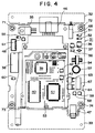
- FIG. 4 is a plan view of the circuit board of the electronic device unit according to the first embodiment of the present invention.
- numeral 31 denotes a circuit board, which is printed with an unillustrated circuit pattern on the front and back surfaces thereof.
- Working plate portions 32 and 33 are formed integrally with the circuit board 31 at both ends (at upper and lower ends in FIG. 4) of the circuit board 31, and are removed after flow soldering is completed.
- circuit board 31 Mounted on the surface of the circuit board 31 are electronic components such as ICs 35 to 43, connectors 46 to 48, diodes 51 to 55, capacitors 56 to 61, power transistors 63 and 64, a resistor 67, and a switch 68.
- the circuit pattern can be formed on either one of the front and back surfaces of the circuit board 31.
- Holes 71 to 74 are formed in the circuit board 31 at four corners thereof, and an unillustrated screw is inserted through each of the holes 71 to 74 to thereby mount the circuit board 31 onto a case.
- FIG. 5 is a plan view of a lower case of the electronic device unit according to the first embodiment of the present invention.
- FIG. 6 is a front view of the lower case of the electronic device unit according to the first embodiment of the present invention.
- FIG. 7 is a plan view of an upper case of the electronic device unit according to the first embodiment of the present invention.
- FIG. 8 is a front view of the upper case of the electronic device unit according to the first embodiment of the present invention.
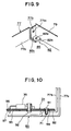
- FIG. 9 is a perspective view of a main portion of the lower case of the electronic device unit according to the first embodiment of the present invention.
- numeral 76 denotes a lower case which is open at its top and front and which is composed of side walls 77 and 78, a rear wall 79, and a bottom panel 85
- numeral 84 denotes an upper case which is open at its bottom and front and which is composed of side walls 87 and 88, a rear wall 89, and a top panel 86.
- the upper case 84 covers the lower case 76 to thereby form the case.
- Both the upper case 84 and the lower case 76 or at least the lower case 76 is made of a highly heat-conductive material such as metal in order to radiate heat conducted from unillustrated electronic components.
- Bases 80 to 83 for mounting the circuit board 31 (FIG. 4) thereon are integrally formed with the bottom panel 85 by bending at the front ends (on the bottom side in FIG. 5) and rear ends (on the top side in FIG. 5) of the bottom panel 85.
- Each of the bases 80 and 81 is formed such that a protrusion having a width w1 and protruding forward from the front end of the bottom panel 85 is raised by a height h1.
- the bases 80 and 81 are composed of vertical portions 80b and 81b and horizontal portions 80c and 81c, respectively. Holes 80a and 81a are formed in the horizontal portions 80c and 81c, respectively.
- Each of the bases 82 and 83 is formed such that a strip having a width w2 and formed by cutting the side wall 77 or 78 and the bottom panel 85 is raised by a height h1.
- the bases 82 and 83 are composed of vertical portions 82b and 83b and horizontal portions 82c and 83c, respectively. Holes 82a and 83a are formed in the horizontal portions 82c and 83c, respectively.
- the side walls 77 and 78 are composed of central portions 77a and 78a, rear portions 77b and 78b, and front portions 77c and 78c, respectively.
- the rear portions 77b and 78b and the front portions 77c and 78c are displaced inward from the central portions 77a and 78a by a dimension w3.
- Holes 77b 1 and 78b 1 are formed in the rear portions 77b and 78b, respectively, while holes 77c 1 and 78c 1 are formed in the front portions 77c and 78c, respectively.
- a depression 87b is formed at a position corresponding to the hole 77b 1
- a depression 87c is formed at a position corresponding to the hole 77c 1
- a depression 88b is formed at a position corresponding to the hole 78b 1
- a depression 88c is formed at a position corresponding to the hole 78c 1 .
- An unillustrated hole is formed in each of the depressions 87b, 87c, 88b, and 88c.
- the depth of the depressions 87b, 87c, 88b, and 88c is identical to the widthwise dimension w3.
- the holes of the depressions 87b, 87c, 88b, and 88c are aligned with the holes 77b 1 , 77c 1 , 78b 1 , and 78c 1 , respectively, so that the upper case 84 and the lower case 76 can be fastened together by screw engagement through use of unillustrated screws. Since the head portions of the screws are accommodated within the depressions 87b, 87c, 88b, and 88c, the appearance of the case is improved.
- the IC 35 is a three-terminal regulator
- the ICs 36 and 37 are power amplifiers.
- the power transistors 63 and 64 generate heat when operated.
- the thus-generated heat is conducted to the case via the circuit board 31 and radiated from the case.
- FIG. 10 is a sectional view showing the mounting of an electronic component according to the first embodiment of the present invention.
- FIG. 11 is a perspective view showing the mounting of the electronic component according to the first embodiment of the present invention.
- a base 82 is formed at a corner of a base panel 85.
- a circuit board 31 is fixed onto the base 82 by a screw 91, which serves as fixing means.
- An electronic component such as an IC 35 is fixed onto the circuit board 31 by a screw 92.
- the circuit board 31 is composed of a board 95 having an insulating property and circuit patterns 96 and 97, which are formed by printing on the front and back surfaces, respectively, of the board 95.
- the circuit patterns 96 and 97 are each composed of an unillustrated circuit portion and an unillustrated heat conduction portion.
- the circuit portion is electrically connected to unillustrated terminals of each electronic component, and includes a common bus, various signal lines, and the like.
- the heat conduction portion is electrically insulated from the circuit portion and is formed in a solid pattern at a region other than that of the circuit portion.
- the heat conduction portion serves as a heat sink.
- the heat conduction portion of the circuit pattern 96 is connected to that of the circuit pattern 97 by means of through holes 99, each of which being formed in the holes 71 to 74 (FIG. 4).
- the inner wall surface of the through hole 99 is plated with metal to thereby connect the heat conduction portions together.
- Numeral 77a denotes the central portion of the side wall 77 of the lower case 76 (FIG. 5).
- Numeral 77b denotes the rear portion of the side wall 77.
- Numeral 79 denotes the rear wall of the lower case 76.
- the bottom surface of the electronic component is brought into contact with the heat conduction portion of the circuit pattern 96. Accordingly, the heat generated within the operated electronic component is sequentially conducted to the heat conduction portion of the circuit pattern 96, the through holes 99 formed in the holes 71 to 74, the heat conduction portion of the circuit pattern 97, and the bases 80 to 83, and is then radiated from the lower case 76.
- the bases 80 to 83 are integrally formed with the bottom panel 85 through bending, the area in which the bases 80 to 83 contact with the heat conduction portion of the circuit pattern 97 can be increased. Accordingly, heat conductivity can be improved.
- the heat conduction portions of the circuit patterns 96 and 97 serve as a heat sink, so that not only can the number of components be reduced, but also processes required for assembly can be reduced, resulting in a lower manufacturing cost of the electronic device unit.
- the appearance of the case improves, and the electronic component can be readily positioned without the use of a dedicated jig when the circuit board is flow-soldered.
- FIG. 12 is a perspective view of a main portion of a lower case according to the second embodiment of the present invention.
- numeral 77 denotes a side wall of a lower case 176
- numeral 79 denotes a rear wall
- numeral 85 denotes a bottom panel
- numeral 182 denotes a base
- numeral 182a denotes a hole formed in the base 182.
- Part of the side wall 77 is cut and bent so as to become parallel with the bottom panel 85. In this case, the number of processes of the bending work can be reduced, so that not only can work be simplified, but also the manufacturing cost of the electronic device unit can be further reduced.
- the bases 80 to 83 and 182 are formed by bending. Alternatively, they may be formed by extrusion. Further alternatively, a metallic piece having a thickness equal to the height of the bases 80 to 83 and 182 may be welded onto the bottom panel 85 so as to serve as a base.
- an electronic component is fixed onto the circuit board 31 (FIG. 10) on the side of the circuit pattern 96.
- the heat generated within the operated electronic component is conducted to the heat conduction portion of the circuit pattern 97 and then to the bases 80 to 83 and 182.
- the through holes 99 are used in the first and second embodiments.
- an edge portion of the circuit board 31 may be plated with metal for thermal conduction.
- the circuit board 31 is fixed onto the bases 80 to 83 and 182 by screw engagement through use of the through holes 99.
- the circuit board 31 may be fixed onto the lower cases 76 and 176 by clipping, soldering, or the like.
- FIG. 13 is a perspective view of a card interface unit according to the third embodiment of the present invention.
- FIG. 14 is a plan view of a main portion of a card insertion guide of the card interface unit according to the third embodiment of the present invention.
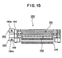
- FIG. 15 is a front view of the main portion of the card insertion guide of the card interface unit according to the third embodiment of the present invention.
- FIG. 16 is a side view of the main portion of the card insertion guide of the card interface unit according to the third embodiment of the present invention.
- numeral 21 denotes a card interface unit
- numeral 122 denotes a slot formed in a front panel 21a of the card interface unit 21.
- the card interface unit 21 two unillustrated PC cards of type I or II can be inserted/removed into/from the slot 122.
- accommodating sections 151 and 152 are formed within the card interface unit 21.
- the card interface unit 21 allows one PC card of type III to be inserted/removed thereinto/therefrom. Hatching P1 in FIG. 14 indicates the end portion of a PC card of type I, II, or III when it is loaded.
- the card insertion guide 150 includes a pair of vertically layered holding frames 154 and 155, which define the accommodating sections 151 and 152, respectively. Three or more holding frames can be vertically layered in order to load three or more PC cards of type I or II into respective accommodating sections.
- Each of the holding frames 154 and 155 is composed of a rear portion 159 and side holding portions 157 and 158, the cross section of each being shaped in a lying squarish letter U.
- the holding portions 157 and 158 hold both side edges of each loaded PC card.
- a side contact 161 and an EMI/ESD contact 162 are disposed on the inner surface of each of the holding portions 157 and 158.
- the side contact 161 is used to ground the case of a PC card, and the EMI/ESD contact 162 serves as a shield terminal against noise.
- Card connectors 171 and 172 are attached to the rear ends (left-hand ends in FIG. 16) of the holding frames 154 and 155, respectively.
- the front end surfaces of the card connectors 171 and 172 are electrically connected to the rear ends of the respective PC cards.
- a plurality of L-shaped lead wires 175 project from the rear end surfaces of the card connectors 171 and 172. The lead wires 175 establish the electrical connection between the card insertion guide 150 and the circuit board.
- Two eject buttons 183 and 184 are disposed alongside the slot 122 in the front panel 21a such that their front ends project from the front panel 21a.
- a press of the eject button 183 or 184 causes the corresponding PC card to be ejected independently of the other PC card.
- eject mechanisms 133 and 134 are disposed adjacently to the holding frames 154 and 155, respectively.
- the eject button 183 or 184 is pressed to operate the corresponding eject mechanism 133 or 134, this pressing operation is transmitted to the rear end of the corresponding PC card.
- the eject mechanism 133 includes a shaft 135 (136) extending backward (to the left in FIG. 16) within the card interface unit 21 and an unillustrated eject arm disposed within the card interface unit 21 in the vicinity of the rear wall of the card interface unit 21.
- the eject buttons 183 and 184 are integrally formed with the shafts 135 and 136, respectively, at their front ends.
- One end of the eject arm is linked with the rear end of the shaft 135 (136). The other end of the eject arm abuts the rear end of the corresponding PC card.
- the shafts 135 and 136 are slidably supported by the holding frames 154 and 155, respectively.
- elongated grooves 191 and 192 are formed in each of the shafts 135 and 136, and are respectively engaged with protrusions 193 and 194 formed on the side wall of each of the holding frames 154 and 155.
- the elongated groove 191 is composed of a wide slide portion 191a and narrow slits 191b which continuously extend from both ends of the slide portion 191a.
- the width of the tip of the protrusion 193 is slightly wider than that of the slide portion 191a. Accordingly, the protrusion 193 is inserted into the slide portion 191a while causing the slit 191b to expand.
- the elongated groove 192 is composed of a wide slide portion 192a and a narrow slit 192b which continuously extends from one end of the slide portion 192a.
- the width of the tip of the protrusion 194 is slightly wider than that of the slide portion 192a. Accordingly, the protrusion 194 is inserted into the slide portion 192a while causing the slit 192b to expand.
- the shaft 135 is attached to and held by the holding frame 154, while the shaft 136 is attached to and held by the holding frame 155.
- a PC card of type III is loaded into the accommodating section 152.
- the eject button 184 When the eject button 184 is pressed, the PC card of type III is ejected.
- two PC cards of type I or II can be loaded in a manner lying one on the other into the single slot 122, and also the eject mechanisms 133 and 134 are respectively disposed alongside the accommodating sections 151 and 152 so as to eject the PC cards independently of each other. Accordingly, the eject mechanisms 133 and 134 are disposed quite close to each other.
- stepped portions 196 and 197 are formed between the eject button 183 and the shaft 135 and between the eject button 184 and the shaft 136, respectively, behind as well as in the vicinity of the front panel 21a, whereby a press portion 183a of the eject button 183 is displaced upward from the shaft 135, and a press portion 184a of the eject button 184 is displaced downward from the shaft 136. Accordingly, the press portions 183a and 184a can be positioned sufficiently apart from each other.
- the stepped portions 196 and 197 are formed between the eject button 183 and the shaft 135 and between the eject button 184 and the shaft 136, respectively.
- stepped portions may be formed in the eject buttons 183 and 184 themselves, or in the vicinity of the front ends of the shafts 135 and 136 themselves.
- sloped portions or curved portions may be formed in place of the stepped portions 196 and 197.
- the eject buttons 183 and 184 are integrally formed with the shafts 135 and 136, respectively.
- the eject buttons may be formed separately from the shafts and fixed to them by unillustrated fixing means.
- the press portions 183a and 184a are displaced from the shafts 135 and 136, respectively.
- either one of the press portions 183a and 184a may be displaced from the corresponding shaft.
- a PC card can be ejected without fail.
- the portion of the front panel 21a between the press portions 183a and 184a serves as a rib, thereby increasing the strength of the front panel 21a.
- the press portions 183a and 184a of the two eject buttons 183 and 184, respectively, are disposed sufficiently apart from each other. Even when three or more holding frames are arranged in vertical layers, the press portions of three or more eject buttons can be disposed sufficiently apart from each other.
Landscapes
- Engineering & Computer Science (AREA)
- Microelectronics & Electronic Packaging (AREA)
- Casings For Electric Apparatus (AREA)
- Coupling Device And Connection With Printed Circuit (AREA)
- Structures For Mounting Electric Components On Printed Circuit Boards (AREA)
Applications Claiming Priority (4)
| Application Number | Priority Date | Filing Date | Title |
|---|---|---|---|
| JP100483/96 | 1996-04-22 | ||
| JP10048396A JPH09289389A (ja) | 1996-04-22 | 1996-04-22 | 電子機器ユニット |
| JP107746/96 | 1996-04-26 | ||
| JP8107746A JPH09293127A (ja) | 1996-04-26 | 1996-04-26 | カードインタフェースユニット |
Publications (2)
| Publication Number | Publication Date |
|---|---|
| EP0804062A2 true EP0804062A2 (fr) | 1997-10-29 |
| EP0804062A3 EP0804062A3 (fr) | 1998-10-14 |
Family
ID=26441497
Family Applications (1)
| Application Number | Title | Priority Date | Filing Date |
|---|---|---|---|
| EP96120889A Withdrawn EP0804062A3 (fr) | 1996-04-22 | 1996-12-27 | Unité d'un dispositif électronique |
Country Status (2)
| Country | Link |
|---|---|
| EP (1) | EP0804062A3 (fr) |
| KR (1) | KR970014503A (fr) |
Families Citing this family (1)
| Publication number | Priority date | Publication date | Assignee | Title |
|---|---|---|---|---|
| KR102272423B1 (ko) | 2015-01-14 | 2021-07-02 | 삼성디스플레이 주식회사 | 유기 발광 표시 장치 |
Family Cites Families (2)
| Publication number | Priority date | Publication date | Assignee | Title |
|---|---|---|---|---|
| DE4304050A1 (de) * | 1993-02-11 | 1994-08-18 | Bosch Gmbh Robert | Gehäuse für eine elektronische Schaltung |
| DE19506664A1 (de) * | 1995-02-25 | 1996-02-29 | Bosch Gmbh Robert | Elektrisches Gerät |
-
1996
- 1996-12-27 EP EP96120889A patent/EP0804062A3/fr not_active Withdrawn
- 1996-12-31 KR KR1019960081141A patent/KR970014503A/ko not_active Ceased
Non-Patent Citations (1)
| Title |
|---|
| None |
Also Published As
| Publication number | Publication date |
|---|---|
| EP0804062A3 (fr) | 1998-10-14 |
| KR970014503A (ko) | 1997-03-29 |
Similar Documents
| Publication | Publication Date | Title |
|---|---|---|
| US5398154A (en) | Card grounding apparatus | |
| US5017156A (en) | Electrical connector | |
| US6224391B1 (en) | Memory card adaptor card | |
| US6793536B2 (en) | Contact terminal and card connector having the same | |
| US5775949A (en) | Compact smart card receiver | |
| US9585280B2 (en) | Electronic modular unit, in particular capacitive proximity sensor for a vehicle and method of producing the modular unit | |
| US6343956B2 (en) | Circuit board mounted connector ground | |
| JP7348087B2 (ja) | コネクタ | |
| JP2020187844A (ja) | ホストコネクタ、および、それを備えるリセプタクルアセンブリー | |
| US6361338B1 (en) | Electrical card connector | |
| US7775835B2 (en) | Electrical card connector | |
| US6099321A (en) | Low profile zero insertion force socket | |
| KR940002899B1 (ko) | 전기 콘넥터 | |
| US5562461A (en) | Circuit board electrical connector | |
| US6247946B1 (en) | Card connector comprising connector portion and separatable card-receiving frame portion with card ejector mechanism | |
| JP3743618B2 (ja) | カード用コネクタ組立体 | |
| JP2000340305A (ja) | 外部インターフェースコネクタの接地構造 | |
| JPS61110981A (ja) | 電気素子アセンブリユニツト用後壁配線装置 | |
| JP3278052B2 (ja) | シールドコネクタ | |
| JPH07176882A (ja) | 冷却ファンの実装構造 | |
| JP4266838B2 (ja) | 電子鍵盤楽器の電子部品取付構造 | |
| US6508657B2 (en) | Connector | |
| US6290541B1 (en) | Connector for IC card, having shielding plates | |
| US7389924B2 (en) | Electronic card connector | |
| US6336828B1 (en) | Power bus bar docking mechanism |
Legal Events
| Date | Code | Title | Description |
|---|---|---|---|
| PUAI | Public reference made under article 153(3) epc to a published international application that has entered the european phase |
Free format text: ORIGINAL CODE: 0009012 |
|
| 17P | Request for examination filed |
Effective date: 19970124 |
|
| AK | Designated contracting states |
Kind code of ref document: A2 Designated state(s): DE FR GB IT |
|
| PUAL | Search report despatched |
Free format text: ORIGINAL CODE: 0009013 |
|
| AK | Designated contracting states |
Kind code of ref document: A3 Designated state(s): DE FR GB IT |
|
| STAA | Information on the status of an ep patent application or granted ep patent |
Free format text: STATUS: THE APPLICATION HAS BEEN WITHDRAWN |
|
| 18W | Application withdrawn |
Withdrawal date: 19981021 |