EP0805447A2 - Egalisation adaptive et récupération d'horloge interpolée dans un canal de lecture échantillonné en amplitude pour l'enregistrement magnétique - Google Patents
Egalisation adaptive et récupération d'horloge interpolée dans un canal de lecture échantillonné en amplitude pour l'enregistrement magnétique Download PDFInfo
- Publication number
- EP0805447A2 EP0805447A2 EP97104311A EP97104311A EP0805447A2 EP 0805447 A2 EP0805447 A2 EP 0805447A2 EP 97104311 A EP97104311 A EP 97104311A EP 97104311 A EP97104311 A EP 97104311A EP 0805447 A2 EP0805447 A2 EP 0805447A2
- Authority
- EP
- European Patent Office
- Prior art keywords
- filter
- sample values
- sampled amplitude
- recited
- interpolated
- Prior art date
- Legal status (The legal status is an assumption and is not a legal conclusion. Google has not performed a legal analysis and makes no representation as to the accuracy of the status listed.)
- Withdrawn
Links
Images







Classifications
-
- G—PHYSICS
- G11—INFORMATION STORAGE
- G11B—INFORMATION STORAGE BASED ON RELATIVE MOVEMENT BETWEEN RECORD CARRIER AND TRANSDUCER
- G11B20/00—Signal processing not specific to the method of recording or reproducing; Circuits therefor
- G11B20/10—Digital recording or reproducing
- G11B20/10009—Improvement or modification of read or write signals
- G11B20/10046—Improvement or modification of read or write signals filtering or equalising, e.g. setting the tap weights of an FIR filter
-
- G—PHYSICS
- G11—INFORMATION STORAGE
- G11B—INFORMATION STORAGE BASED ON RELATIVE MOVEMENT BETWEEN RECORD CARRIER AND TRANSDUCER
- G11B20/00—Signal processing not specific to the method of recording or reproducing; Circuits therefor
- G11B20/10—Digital recording or reproducing
- G11B20/10009—Improvement or modification of read or write signals
- G11B20/10046—Improvement or modification of read or write signals filtering or equalising, e.g. setting the tap weights of an FIR filter
- G11B20/10194—Improvement or modification of read or write signals filtering or equalising, e.g. setting the tap weights of an FIR filter using predistortion during writing
-
- G—PHYSICS
- G11—INFORMATION STORAGE
- G11B—INFORMATION STORAGE BASED ON RELATIVE MOVEMENT BETWEEN RECORD CARRIER AND TRANSDUCER
- G11B20/00—Signal processing not specific to the method of recording or reproducing; Circuits therefor
- G11B20/10—Digital recording or reproducing
- G11B20/10009—Improvement or modification of read or write signals
- G11B20/10037—A/D conversion, D/A conversion, sampling, slicing and digital quantisation or adjusting parameters thereof
-
- G—PHYSICS
- G11—INFORMATION STORAGE
- G11B—INFORMATION STORAGE BASED ON RELATIVE MOVEMENT BETWEEN RECORD CARRIER AND TRANSDUCER
- G11B20/00—Signal processing not specific to the method of recording or reproducing; Circuits therefor
- G11B20/10—Digital recording or reproducing
- G11B20/10009—Improvement or modification of read or write signals
- G11B20/10046—Improvement or modification of read or write signals filtering or equalising, e.g. setting the tap weights of an FIR filter
- G11B20/10055—Improvement or modification of read or write signals filtering or equalising, e.g. setting the tap weights of an FIR filter using partial response filtering when writing the signal to the medium or reading it therefrom
-
- G—PHYSICS
- G11—INFORMATION STORAGE
- G11B—INFORMATION STORAGE BASED ON RELATIVE MOVEMENT BETWEEN RECORD CARRIER AND TRANSDUCER
- G11B20/00—Signal processing not specific to the method of recording or reproducing; Circuits therefor
- G11B20/10—Digital recording or reproducing
- G11B20/18—Error detection or correction; Testing, e.g. of drop-outs
- G11B20/1876—Interpolating methods
-
- G—PHYSICS
- G11—INFORMATION STORAGE
- G11B—INFORMATION STORAGE BASED ON RELATIVE MOVEMENT BETWEEN RECORD CARRIER AND TRANSDUCER
- G11B20/00—Signal processing not specific to the method of recording or reproducing; Circuits therefor
- G11B20/10—Digital recording or reproducing
- G11B20/12—Formatting, e.g. arrangement of data block or words on the record carriers
- G11B20/1217—Formatting, e.g. arrangement of data block or words on the record carriers on discs
- G11B20/1258—Formatting, e.g. arrangement of data block or words on the record carriers on discs where blocks are arranged within multiple radial zones, e.g. Zone Bit Recording or Constant Density Recording discs, MCAV discs, MCLV discs
Definitions
- the present invention relates to the control of magnetic disk storage systems for digital computers, particularly to a sampled amplitude read channel that employs asynchronous sampling of an analog read signal, adaptive discrete time equalization, and interpolated timing recovery.
- digital data serves to modulate the current in a read/write head coil in order to write a sequence of corresponding magnetic flux transitions onto the surface of a magnetic medium in concentric, radially spaced tracks at a predetermined baud rate.
- the read/write head again passes over the magnetic medium and transduces the magnetic transitions into pulses in an analog read signal that alternate in polarity. These pulses are then decoded by read channel circuitry to reproduce the digital data.
- Decoding the pulses into a digital sequence can be performed by a simple peak detector in a conventional analog read channel or, as in more recent designs, by a discrete time sequence detector in a sampled amplitude read channel.
- Discrete time sequence detectors are preferred over simple analog pulse detectors because they compensate for intersymbol interference (ISI) and are less susceptible to channel noise. As a result, discrete time sequence detectors increase the capacity and reliability of the storage system.
- ISI intersymbol interference
- DPD discrete time pulse detection
- PR partial response
- MLSD maximum likelihood sequence detection
- DFE decision-feedback equalization
- EDFE enhanced decision-feedback equalization
- FDTS/DF fixed-delay tree-search with decision-feedback
- analog circuitry responsive to threshold crossing or derivative information, detects peaks in the continuous time analog signal generated by the read head.
- the analog read signal is "segmented” into bit cell periods and interpreted during these segments of time. The presence of a peak during the bit cell period is detected as a "1" bit, whereas the absence of a peak is detected as a "0" bit.
- Timing recovery then, adjusts the bit cell periods so that the peaks occur in the center of the bit cells on average in order to minimize detection errors. Since timing information is derived only when peaks are detected, the input data stream is normally run length limited (RLL) to limit the number of consecutive "0" bits.
- RLL run length limited
- detection errors can also occur due to intersymbol interference, a distortion in the read signal caused by closely spaced overlapping pulses. This interference can cause a peak to shift out of its bit cell, or its magnitude to decrease, resulting in a detection error.
- the ISI effect is reduced by decreasing the data density or by employing an encoding scheme that ensures a minimum number of "0" bits occur between "1" bits.
- a (d,k) run length limited (RLL) code constrains to d the minimum number of "0" bits between "1” bits, and to k the maximum number of consecutive "0" bits.
- RLL 2/3 rate code encodes 8 bit data words into 12 bit codewords to satisfy the (1,7) constraint.
- Sampled amplitude detection such as partial response (PR) with Viterbi detection, allows for increased data density by compensating for intersymbol interference and the effect of channel noise.
- sampled amplitude recording detects digital data by interpreting, at discrete time instances, the actual value of the pulse data.
- the read channel comprises a sampling device for sampling the analog read signal, and a timing recovery circuit for synchronizing the samples to the baud rate (code bit rate).
- a variable gain amplifier adjusts the read signal's amplitude to a nominal value, and a low pass analog filter filters the read signal to attenuate aliasing noise.
- a digital equalizer filter After sampling, a digital equalizer filter equalizes the sample values according to a desired partial response, and a discrete time sequence detector, such as a Viterbi detector, interprets the equalized sample values in context to determine a most likely sequence for the digital data (i.e., maximum likelihood sequence detection (MLSD)).
- MLSD takes into account the effect of ISI and channel noise in the detection algorithm, thereby decreasing the probability of a detection error. This increases the effective signal to noise ratio and, for a given (d,k) constraint, allows for significantly higher data density as compared to conventional analog peak detection read channels.
- sampled amplitude detection requires timing recovery in order to correctly extract the digital sequence. Rather than process the continuous signal to align peaks to the center of bit cell periods as in peak detection systems, sampled amplitude systems synchronize the pulse samples to the baud rate. In conventional sampled amplitude read channels, timing recovery synchronizes a sampling clock by minimizing an error between the signal sample values and estimated sample values. A pulse detector or slicer determines the estimated sample values from the read signal samples. Even in the presence of ISI the sample values can be estimated and, together with the signal sample values, used to synchronize the sampling of the analog pulses in a decision-directed feedback system.
- a phase-locked-loop normally implements the timing recovery decision-directed feedback system.
- the PLL comprises a phase detector for generating a phase error based on the difference between the estimated samples and the read signal samples.
- a PLL loop filter filters the phase error, and the filtered phase error operates to synchronize the channel samples to the baud rate.
- the phase error adjusts the frequency of a sampling clock which is typically the output of a variable frequency oscillator (VFO).
- VFO variable frequency oscillator
- the output of the VFO controls a sampling device, such as an analog-to-digital (A/D) converter, to synchronize the sampling to the baud rate.
- A/D analog-to-digital
- sampled amplitude read channels also commonly employ a discrete time equalizer filter to equalize the sample values into a desired partial response (PR4, EPR4, EEPR4, etc.) before sequence detection.
- PR4, EPR4, EEPR4, etc. a desired partial response
- adaptive algorithms have been applied to compensate in real time for parameter variations in the recording system and across the disk radius.
- a problem associated with adaptive equalizer filters in sampled amplitude read channels is that the timing recovery and gain control loops can interfere with the adaptive feedback loop, thereby preventing the adaptive equalizer filter from converging to an optimal state. This non-convergence is manifested by the filter's phase and gain response drifting as it competes with the timing and gain control loops.
- Constraining the phase response of the adaptive equalizer in this manner is a very sub-optimal method for attenuating interference from the timing recovery and gain control loops. Furthermore, it significantly reduces control over the adaptive filter's phase response, thereby placing the burden of phase compensation on the analog equalizer.
- a further aspect of the present invention is to remove the adaptive equalizer, and its associated latency, from the timing recovery loop, thereby allowing a higher order discrete time filter and a simplified analog filter.
- a sampled amplitude read channel for magnetic disk recording which asynchronously samples the analog read signal, adaptively equalizes the resulting discrete time sample values according to a target partial response, extracts synchronous sample values through interpolated timing recovery, and detects digital data from the synchronous sample values using a Viterbi sequence detector is disclosed.
- the phase and magnitude response of the adaptive equalizer filter are constrained at a predetermined frequency using an optimal orthogonal projection operation as a modification to a least mean square (LMS) adaptation algorithm.
- LMS least mean square
- FIG. 1 shown is a detailed block diagram of a conventional sampled amplitude read channel.
- a data generator 4 for example 2T preamble data
- An RLL encoder 6 encodes the user data 2 into a binary sequence b(n) 8 according to an RLL constraint.
- a precoder 10 precodes the binary sequence b(n) 8 in order to compensate for the transfer function of the recording channel 18 and equalizer filters to form a precoded sequence ⁇ b(n) 12 .
- Write circuitry 9 responsive to the symbols a(n) 16 , modulates the current in the recording head coil at the baud rate 1/T to record the binary sequence onto the media.
- a frequency synthesizer 52 provides a baud rate write clock 54 to the write circuitry 9 and is adjusted by a channel data rate signal (CDR) 30 according to the zone the recording head is over.
- CDR channel data rate signal
- timing recovery 28 When reading the recorded binary sequence from the media, timing recovery 28 first locks to the write frequency by selecting, as the input to the read channel, the write clock 54 through a multiplexor 60 . Once locked to the write frequency, the multiplexor 60 selects the signal 19 from the read head as the input to the read channel in order to acquire an acquisition preamble recorded on the disk prior to the recorded user data.
- a variable gain amplifier 22 adjusts the amplitude of the analog read signal 58 , and an analog filter 20 provides initial equalization toward the desired response as well as attenuating aliasing noise.
- a sampling device 24 samples the analog read signal 62 from the analog filter 20 , and a discrete time equalizer filter 26 provides further equalization of the sample values 25 toward the desired response. In partial response recording, for example, the desired response is often selected from Table 1.
- the discrete equalizer filter 26 may be implemented as a real-time adaptive filter which compensates for parameter variations over the disk radius (i.e., zones), disk angle, and environmental conditions such as temperature drift. To this end, the filter 26 receives estimated sample values B143 generated by the timing recovery circuit 28 ; the estimated samples being input into an adaptive feedback loop and used to generate sample errors.
- the adaptive feedback loop conventionally employs a least mean square (LMS) algorithm to adapt the filter coefficients (i.e., it adapts the frequency and phase response of the filter) until a minimum sample error is achieved. Operation of a conventional adaptive equalizer filter is discussed in greater detail below.
- LMS least mean square
- the equalized sample values 32 are applied to a decision directed gain control 50 and timing recovery 28 circuit for adjusting the amplitude of the read signal 58 and the frequency and phase of the sampling device 24 , respectively.
- Timing recovery adjusts the frequency of sampling device 24 over line 23 in order to synchronize the equalized samples 32 to the baud rate.
- Frequency synthesizer 52 provides a course center frequency setting to the timing recovery circuit 28 over line 64 in order to center the timing recovery frequency over temperature, voltage, and process variations.
- the channel data rate (CDR) 30 signal adjusts a frequency range of the synthesizer 52 according to the data rate for the current zone.
- Gain control 50 adjusts the gain of variable gain amplifier 22 over line 21 in order to match the magnitude of the channel's frequency response to the desired partial response.
- the equalized samples Y(n) 32 are also sent to a discrete time sequence detector 34 , such as a maximum likelihood (ML) Viterbi sequence detector, which detects an estimated binary sequence ⁇ b(n) 33 from the sample values.
- An RLL decoder 36 decodes the estimated binary sequence ⁇ b(n) 33 from the sequence detector 34 into estimated user data 37 .
- a data sync detector 66 detects the sync mark 70 (shown in FIG. 2B) in the data sector 15 in order to frame operation of the RLL decoder 36 .
- the estimated binary sequence ⁇ b(n) 33 matches the recorded binary sequence b(n) 8
- the decoded user data 37 matches the recorded user data 2 .
- FIG. 2A shows an exemplary data format of a magnetic media comprising a series of concentric data tracks 13 wherein each data track 13 comprises a plurality of sectors 15 with embedded servo wedges 17 .
- a servo controller (not shown) processes the servo data in the servo wedges 17 and, in response thereto, positions the read/write head over a desired track. Additionally, the servo controller processes servo bursts within the servo wedges 17 to keep the head aligned over a centerline of the desired track while writing and reading data.
- the servo wedges 17 may be detected by a simple discrete time pulse detector or by the discrete time sequence detector 34 . If the sequence detector 34 detects the servo data, then the format of the servo wedges 17 includes a preamble and a sync mark, similar to the user data sectors 15 .
- FIG. 2B shows the format of a user data sector 15 comprising an acquisition preamble 68 , a sync mark 70 , and user data 72 .
- Timing recovery uses the acquisition preamble 68 to acquire the correct sampling frequency and phase before reading the user data 72
- the sync mark 70 demarks the beginning of the user data 72 (see co-pending U.S. patent application 08/313,491 entitled "Improved Timing Recovery For Synchronous Partial Response Recording").
- the disk is partitioned into an outer zone 11 comprising fourteen data sectors per track, and an inner zone 27 comprising seven data sectors per track.
- the disk is actually partitioned into several zones with a different number of sectors in each zone, and the data recorded and detected at a different data rate in each zone.
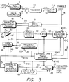
- FIG. 3 shows the improved sampled amplitude read channel of the present invention wherein the conventional sampled timing recovery 28 of FIG. 1 has been replaced by interpolated timing recovery B100 .
- the write frequency synthesizer 52 generates a baud rate write clock 54 applied to the write circuitry 9 , and an asynchronous read clock 54 for clocking the sampling device 24 , the discrete time equalizer filter 26 , and the interpolated timing recovery B100 at a frequency relative to the current zone (CDR 30 ).
- a first frequency synthesizer generates the write clock
- a second frequency synthesizer generates the read clock.
- the discrete equalizer filter B103 is real-time adaptive, receiving interpolated sample values B102 and estimated sample values B143 from the interpolated timing recovery circuit B100 for use in a modified least mean square (LMS) algorithm which constrains the filter's gain and phase response according to the present invention, the details of which are set forth below.
- LMS modified least mean square
- the interpolated timing recovery B100 interpolates the equalized sample values 32 to generate interpolated sample values B102 substantially synchronized to the data rate of the current zone.
- a discrete time sequence detector 34 detects an estimated binary sequence 33 representing the user data from the interpolated sample values B102 .
- the interpolated timing recovery B100 circuit generates a synchronous data clock B104 for clocking operation of the gain control 50 , discrete time sequence detector 34 , sync mark detector 66 and RLL decoder 36 .
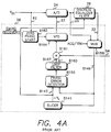
- FIG. 4A An overview of the conventional sampling timing recovery 28 of FIG. 1 is shown in FIG. 4A.
- the output 23 of a variable frequency oscillator (VFO) B164 controls the sampling clock of a sampling device 24 which is typically an analog-to-digital converter (A/D) in digital read channels.
- a multiplexor B159 selects the unequalized sample values 25 during acquisition and the equalized sample values 32 during tracking, thereby removing the discrete equalizer filter 26 from the timing loop during acquisition in order to avoid its associated latency.
- a loop filter B160 filters the phase error to generate a frequency offset ⁇ f B167 that settles to a value proportional to a frequency difference between the sampling clock 23 and the baud rate.
- the frequency offset ⁇ f B167 together with the center frequency control signal 64 from the frequency synthesizer 52 , adjust the sampling clock 23 at the output of the VFO B164 in order to synchronize the sampling to the baud rate.
- a zero phase start B162 circuit suspends operation of the VFO B164 at the beginning of acquisition in order to minimize the initial phase error between the sampling clock 23 and the read signal 62 . This is achieved by disabling the VFO B164 , detecting a zero crossing in the analog read signal 62 , and re-enabling the VFO 164 after a predetermined delay between the detected zero crossing and the first baud rate sample.
- the estimated sample values B143 at The output of the slicer B141 are also input into the discrete time equalizer filter 26 of FIG. 1 for use in a conventional least mean square (LMS) adaptation algorithm as is described in more detail below.
- LMS least mean square
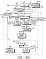
- the interpolated timing recovery B100 of the present invention is shown in FIG. 4B.
- the VFO B164 in the conventional timing recovery of FIG. 4A is replaced with a modulo-Ts accumulator B120 and an interpolator B122 .
- an expected sample value generator B151 responsive to interpolated sample values B102 , generates expected samples Y k+ ⁇ used by the phase error detector B155 to compute the phase error during acquisition.
- a multiplexor B153 selects the estimated sample values ⁇ Y k+ ⁇ from the slicer B141 for use by the phase error detector B155 during tracking.
- the data clock B104 is generated at the output of an AND gate B126 in response to the sampling clock 54 and a mask signal B124 from the modulo-Ts accumulator B120 as discussed in further detail below.
- the phase error detector B155 and the slicer B141 process interpolated sample values B102 at the output of the interpolator B122 rather than the channel sample values 32 at the output of the discrete equalizer filter 26 as in FIG. 4A.
- a PID loop filter B161 controls the closed loop frequency response similar to the loop filter B160 of FIG. 4A.
- the interpolated sample values Y k+ ⁇ B102 and the estimated sample values ⁇ Y k+ ⁇ from the slicer B141 are input into the adaptive, discrete equalizer filter B103 of FIG. 3 for use by a modified least mean square (LMS) algorithm, the details of which are set forth below.
- LMS modified least mean square
- a zero phase start circuit B163 minimizes the initial phase error between the interpolated sample values and the baud rate at the beginning of acquisition similar to the zero phase start circuit B162 of FIG. 4A.
- the zero phase start circuit B163 for interpolated timing recovery computes an initial phase error ⁇ from the A/D 24 sample values 25 and loads this initial phase error into the modulo-Ts accumulator B120 .
- the interpolator B122 of FIG. 4B is understood with reference to FIG. 5 which shows a sampled 2T acquisition preamble signal B200 .
- the target synchronous sample values B102 are shown as black circles and the asynchronous channel sample values 32 as vertical arrows.
- Beneath the sampled preamble signal is a timing diagram depicting the corresponding timing signals for the sampling clock 54 , the data clock B104 and the mask signal B124 .
- the preamble signal B200 is sampled slightly faster than the baud rate (the rate of the target values).
- the function of the interpolator is to estimate the target sample value by interpolating the channel sample values.
- channel sample values B202 and B204 are used to generate the interpolated sample value corresponding to target sample value B206 .
- the interpolation interval ⁇ B208 is generated according to equation (2) above.
- the next interpolated sample value corresponding to the next target value B210 is computed from channel sample values B204 and B212 .
- This process continues until the interpolation interval ⁇ B214 would be greater than Ts except that it "wraps" around and is actually ⁇ B216 (i.e., the accumulated frequency offset ⁇ f , integer divided by Ts, increments by 1 causing the mask signal B124 to activate).
- the data clock B104 is masked by mask signal B124 so that the interpolated sample value corresponding to the target sample value B220 is computed from channel sample values B222 and B224 rather than channel sample values B218 and B222 .
- the interpolator B122 is implemented as a filter responsive to more than two channel samples to compute the interpolated sample value.
- the above non-causal infinite impulse response (4) cannot be realized. Therefore, the impulse response of the interpolation filter is designed to be a best fit approximation of the ideal impulse response (4). This can be accomplished by minimizing a mean squared error between the frequency response of the actual interpolation filter and the frequency response of the ideal interpolation filter (3).
- X( e j ⁇ ) is the spectrum of the read channel (e.g., PR4, EPR4, EEPR4 of Table 1 or some other partial response spectrum).
- equation (6) is modified by specifying that the spectrum of the input signal is bandlimitted to some predetermined constant 0 ⁇ ⁇ ⁇ ⁇ where 0 ⁇ ⁇ ⁇ 1; that is:
- 0, for
- the solution to the minimization problem of equation (7) involves expressing the actual interpolation filter in terms of its coefficients and then solving for the coefficients that minimize the error in a classical mean-square sense.
- a mathematical derivation for an interpolation filter having an even number of coefficients is provided below. It is within the ability of those skilled in the art to modify the mathematics to derive an interpolation filter having an odd number of coefficients.
- Equation (13) defines a set of 2R linear equations in terms of the coefficients C ⁇ (n).
- the implementation of the six tap FIR filter is shown in FIG. 6.
- a shift register B250 receives the channel samples 32 at the sampling clock rate 54 .
- the filter coefficients C ⁇ (n) are stored in a coefficient register file B252 and applied to corresponding multipliers according to the current value of ⁇ B128 .
- the coefficients are multiplied by the channel samples 32 stored in the shift register B250 .
- the resulting products are summed B254 and the sum stored in a delay register B256 .
- the coefficient register file B252 and the delay register B256 are clocked by the data clock B104 to implement the masking function described above.
- a plurality of static FIR filters having coefficients that correspond to the different values of ⁇ , filter the sample values in the shift register B250 .
- Each filter outputs an interpolation value, and the current value of the interpolation interval ⁇ B128 selects the output of the corresponding filter as the output B102 of the interpolator B122 . Since the coefficients of one filter are not constantly updated as in FIG. 6, this multiple filter embodiment increases the speed of the interpolator B122 and the overall throughput of the read channel.
- the coefficient register file B252 of FIG. 6 computes the filter coefficients C ⁇ (n) in real time as a function of ⁇ .
- the filter coefficients C ⁇ (n) can be computed in real time according to a predetermined polynomial in ⁇ (see, for example, U.S. Pat. No. 4,866,647 issued to Farrow entitled, "A Continuously Variable Digital Delay Circuit," the disclosure of which is hereby incorporated by reference).
- An alternative, preferred embodiment for computing the filter coefficients in real time estimates the filter coefficients according to a reduced rank matrix representation of the coefficients.
- the bank of filter coefficients stored in the coefficient register file B252 can be represented as an MxN matrix A MxN , where N is the depth of the interpolation filter (i.e., the number of coefficients C ⁇ (n) in the impulse response computed according to equation (15)) and M is the number of interpolation intervals (i.e., the number of ⁇ intervals).
- N is the depth of the interpolation filter (i.e., the number of coefficients C ⁇ (n) in the impulse response computed according to equation (15))
- M is the number of interpolation intervals (i.e., the number of ⁇ intervals).
- SVD singular value decomposition
- a MxN F MxN ⁇ G NxN .
- a reduced rank approximation of the A MxN matrix can be formed by reducing the size of the F MxN and G NxN matrices by replacing N with L where L ⁇ N and, preferably, L ⁇ N.
- the convolution process of the interpolation filter can then be carried out, as shown in FIG.
- the G LxN matrix as a bank of FIR filters B260 connected to receive the channel sample values 32 , and the F MxL matrix implemented as a lookup table B262 indexed by ⁇ B128 (as will become more apparent in the following discussion).
- the A MxN matrix can be factored into more than two matrices (i.e., A ⁇ FGH).
- the solution to equation (16) can be derived through a singular value decomposition of the A MxN matrix, comprising the steps of:
- the coefficient register file can compute the interpolation filter coefficients C ⁇ (n) according to equation (17) and then convolve the coefficients C ⁇ (n) with the channel samples U(x) 32 to generate the interpolated sample values B102 synchronized to the baud rate.
- FIG. 7 shows the preferred embodiment of the interpolation filter according to equation (19).
- the function of ⁇ is a polynomial in ⁇
- the matrix G i (n) are the coefficients of the polynomial.
- LMS least mean square
- the desired filter output is the estimated sample values ⁇ Y k at the output of slicer B141 .
- the estimated sample values ⁇ Y k are subtracted from the FIR filter's output Y k to generate the sample error e k .
- the LMS algorithm attempts to minimize the sample error in a least mean square sense by adapting the FIR filter coefficients; that is, it adjusts the FIR filter's gain and phase response so that the overall channel response adequately tracks the desired partial response (e.g., PR4, EPR4, EEPR4, etc.).
- interference from the timing recovery 28 and gain control 50 loops can prevent the adaptive, discrete time equalizer 26 from converging to an optimal state.
- a phase adjustment in the adaptive filter 26 can affect the sampling phase error for timing recovery 28 .
- Timing recovery 28 compensates for the filter's phase adjustment by adjusting its sampling phase; this adjustment can result in yet another phase adjustment by the adaptive equalizer 26 .
- the phase response of the adaptive equalizer may never converge.
- the gain control loop 50 can interfere with the gain response of the adaptive filter 26 and prevent it from converging.
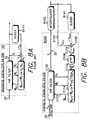
- FIG. 8B illustrates operation of the adaptive, discrete time equalizer filter B103 of the present invention.
- Sample values from the A/D 24 are input over line 25 to a discrete time FIR filter C100 comprising a predetermined number of coefficients, the values of which determine the filter's gain and phase response. Because the FIR filter C100 operates on the sample values prior to the interpolated timing recovery loop B100 , its order can be increased over the prior art without adversely affecting the latency of timing recovery (i.e., the number of filter coefficients can be increased).
- the output Y k 32 of the FIR filter C100 is input into the interpolator B122 for generating the interpolated sample values Y k+ ⁇ B102 .
- the interpolated sample values Y k+ ⁇ B102 are input into a slicer B141 (FIG. 4B) which generates estimated sample values ⁇ Y k+ ⁇ .
- the estimated sample values ⁇ Y k+ ⁇ are subtracted from the interpolated sample values Y k+ ⁇ at adder C102 to generate a sample error value e k+ ⁇ C104 that is synchronized to the baud rate rather than the sample rate.
- the LMS algorithm operates on sample values X k at the sample rate, it is necessary to convert the error value e k+ ⁇ C104 into an error value e k C112 synchronous to the sample rate.
- This is accomplished by an interpolation circuit C106 which computes an interpolated error value e k C112 from the baud rate error values e k+ ⁇ C104 .
- the error value interpolation circuit C106 is implemented as a first order linear interpolation, but it may be a simple zero order hold, or a more complex interpolation filter as described above.
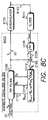
- FIG. 8C shows an alternative embodiment for generating the error value e k .
- the estimated ideal sample values ⁇ Y k+ ⁇ from the slicer B141 are interpolated by the interpolation circuit C106 to generate estimated ideal sample values ⁇ Y k C120 which are subtracted C102 from the equalized sample values Y k 32 at the output of the FIR filter C100 to generate the error value e k
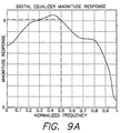
- FIG.s 9A and 9B show an example gain and phase response, respectively, for the FIR filter C100 of the present invention.
- the gain and phase response vary over time as the filter adapts to parameter changes in the recording system; that is, the filter continuously adjusts the channel's overall frequency response so that it matches the desired partial response (PR4, EPR4, EEPR4, etc.) as best possible.
- interference from the timing recovery and gain control loops is attenuated by constraining the gain and phase response of the FIR filter C100 at a predetermined frequency using an orthogonal projection operation Pv 1 v 2 ⁇ .
- the gain (magnitude) response of the FIR filter C100 has been constrained to a predetermined value (denoted by g ) at the normalized frequency of 0.5 (1/4Ts).
- the phase response of the FIR filter C100 has been constrained to k ⁇ at the normalized frequency of 0.5 as shown in FIG. 9B.
- these constraints allow the gain and phase to vary (adapt) at all frequencies except at the normalized frequency of 0.5, thereby constraining the filter's frequency response in a manner that attenuates interference from the gain and timing loops.
- the gain constraint g is relatively arbitrary except that it is selected to optimize the dynamic range of the filter's coefficients.
- constraining the filter's response at the normalized frequency of 0.5 and selecting a phase constraint of k ⁇ reduces the complexity of the orthogonal projection operation Pv 1 v 2 ⁇ , and simplifies implementation of the zero phase start circuit B163 (FIG. 4B) and sync mark detector 66 (FIG. 1).
- the zero phase start circuit B163 minimizes the initial phase error between the interpolated sample values and the baud rate at the beginning of acquisition by computing an initial phase error ⁇ from the A/D 24 sample values 25 and then loading this initial phase error into the modulo-Ts accumulator B120 .
- the zero phase start circuit B163 must take into account the phase delay of the adaptive equalizer filter B103 since interpolated timing recovery B100 operates on the equalized samples 32 , not the A/D 24 samples 25 .
- phase delay of the equalizer B103 will either be zero or 180 0 (i.e., the adjustment to the initial phase error is nothing or a sign change).
- Constraining the phase response of the adaptive equalizer B103 to k ⁇ at the preamble frequency also simplifies implementation of the sync mark detector 66 (FIG. 1) in sampled amplitude read channels that use the conventional synchronous sampling timing recovery 28 (FIG. 4A) rather than interpolated timing recovery B100 (FIG. 4B). Operation of the sync mark detector 66 is described in detail in the above referenced co-pending U.S.
- Patent Application 08/533,797 entitled "Improved Fault Tolerant Sync Mark Detector For sampled Amplitude Magnetic Recording.”
- the sync mark detector 66 is enabled coherent with the end of the acquisition preamble 68 and relative to the transport delay from the output of the A/D 24 to the sync mark detector 66 .
- the transport delay will vary unless the filter's phase response is constrained at the acquisition preamble frequency by, for example, using an orthogonal projection operation Pv 1 v 2 ⁇ of the present invention.
- the equalizer's frequency response at the preamble frequency is, Those skilled in the art will recognize that shifting the time base will lead to four different, but functionally equivalent, frequency responses at the preamble frequency (i.e., [1,-j,-1,j,...] C , [-j,-1,j,1,...] C , [-1,j,1,-j,...] C and [j,1,-j,-1,...] C ).
- the above constraints are achieved by multiplying the computed gradient X k ⁇ e k by an orthogonal projection operation Pv 1 v 2 ⁇ as part of a modified LMS algorithm C114 .
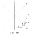
- the orthogonal constraint is not always satisfied as shown in FIG. 10.
- the present invention constrains the filter coefficients to a subspace ⁇ C ⁇ which is orthogonal to V 1 by multiplying the gradient values X k ⁇ e k by a projection operation Pv 1 ⁇ , where the null space of the projection operation Pv 1 ⁇ is orthogonal to ⁇ C ⁇ .
- the updated coefficients correspond to a point on the orthogonal subspace ⁇ C ⁇ closest to the coefficients derived from the unmodified LMS algorithm as shown in FIG. 10.
- the combined orthogonal projection operation Pv 1 v 2 ⁇ eliminates two degrees of freedom in an N-dimensional subspace where N is the number of filter coefficients (i.e., the orthogonal projection operation Pv 1 v 2 ⁇ has a rank of N-2).
- the orthogonal projection operation Pv 1 v 2 ⁇ computed using the above equation for an equalizer comprising ten filter coefficients is a matrix
- the scaling factor is taken into account in the selection of the gain value ⁇ .
- Constraining the gain to g and the phase to k ⁇ at the normalized frequency of 0.5 simplifies implementing the orthogonal projection matrix Pv 1 v 2 ⁇ : half of the elements are zero and the other half are either +1, -1, or +4.
- multiplying the projection matrix Pv 1 v 2 ⁇ by the gradient values X k ⁇ e k requires only shift registers and adders.
- the ACQ/TRK signal shown in FIG. 8B disables adaptation of the FIR filter during acquisition, that is, while acquiring the acquisition preamble 68 shown in FIG. 2B.
- the adaptive equalizer B103 adapts only after acquiring the acquisition preamble 68 .
- an alternative embodiment of the present invention decimates the modified LMS adaptation algorithm C114 as illustrated in FIG.s 11A, 11B, 11C and 11D.
- FIG. 11A implements the above equations (25), (26), (27) and ultimately equation (21) in order to update the coefficients of the equalizer filter C100 according to the modified LMS adaptation algorithm of the present invention.
- the next gradient value g (i)j can be computed by multiplying a sample value latched every tenth clock cycle by the next error value e i .
- the new gradient g (i)j is then used to update the corresponding filter coefficient W (i)j of equation (28).
- the sample values X k are input into the discrete time equalizer filter C100 and the equalized sample values input into the interpolator B122 similar to FIG. 8B.
- a serial-to-parallel circuit C140 converts the interpolated sample values Y k+ ⁇ into even and odd subsequences Y 2k+ ⁇ and Y (2k-1)+ ⁇ , where the notation 2k indicates that two new interpolated sample values are output from the serial-to-parallel circuit C140 at every other sample period.
- a slicer C142 generates the corresponding even and odd estimated subsequences ⁇ Y 2k+ ⁇ and ⁇ Y (2k-1)+ ⁇ which are subtracted from the interpolated sample values at respective adders ( C144 1 , C144 2 ) to form an even and odd sample error sequences e 2k+ ⁇ and e (2k-1)+ ⁇ .
- An error value interpolation circuit C146 similar to that of FIG. 8B, generates the even and odd sample error sequences e 2k and e (2k-1) which are synchronized to the A/D sample rate.
- the circuit of FIG. 11A decimates the adaptation algorithm of the present invention by the number of coefficients in the equalizer filter C100 .
- the output of the delay register C150 X 2k-2j-1 is multiplied by the sample errors e 2k and e (2k-1) at respective multipliers ( C152 1 , C152 2 ) to form the gradient values g 2j and g 2j-1 used in equation (24).
- the gradient values g 2j and g 2j-1 are then shifted into respective shift registers ( C154 1 , C154 2 ).
- the gradient values g 2j and g 2j-1 are multiplied by respective alternating ⁇ 1 ( C156 1 , C156 2 ) and accumulated in respective accumulators ( C158 1 , C158 2 ).
- the outputs of the accumulators (which represent ⁇ 0 and ⁇ 1 of equation (25)) are latched by respective decimate by 5 circuits ( C160 1 , C160 2 ) and the accumulators ( C158 1 , C158 2 ) are reset.
- the values ⁇ 0 and ⁇ 1 are then multiplied by respective alternating ⁇ 1 ( C162 1 , C162 2 ) to implement equation (26).
- the gradient values g 2j and g 2j-1 at the outputs of the shift register ( C154 1 , C154 2 ) are multiplied by 5 ( C164 1 , C164 2 ) and the values ⁇ 0 and ⁇ 1 are subtracted therefrom at adders ( C166 1 , C166 2 ) in order to implement equation (27).
- the output of adders ( C166 1 , C166 2 ) are scaled by a gain factor ⁇ ( C168 1 , C168 2 ) which is reduced by a factor of 5 to account for the scaled up projection operator.
- the output of the gain factor ⁇ ( C168 1 , C168 2 ) is subtracted at adders ( C170 1 , C170 2 ) from the corresponding filter coefficient (W 2j-1 ,W 2j ) selected by a multiplexor ( C172 1 , C172 2 ) from a bank of registers ( C174 1 , C174 2 ).
- the ADAPT 2j signal selects the 2j th coefficient from the bank of registers ( C174 1 , C174 2 ) for updating. After subtracting the update value, the updated filter coefficient ( C176 1 , C176 2 ) is restored to the bank of registers ( C174 1 , C174 2 ) and used by the equalizer filter C100 during the next clock period to equalize the sample values according to its updated spectrum.
- FIG. 11A Decimating the update algorithm by the number of filter coefficients, as in FIG. 11A, decreases the implementation complexity but at the cost of slowing convergence of the equalizer filter C100 toward an optimum setting. This is because the decimated update algorithm does not use all of the sample values to compute the gradients g j .
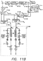
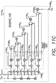
- FIGs. 11B and 11C show an alternative embodiment of the decimated update algorithm of the present invention wherein more of the sample values are used to compute the gradients g j , which adds complexity but improves performance because the equalizer filter C100 converges faster.
- all of the sample values could be used (i.e., a number of sample values equal to the number filter taps), or in an alternative embodiment, a decimated number of sample values could be used in order to reduce the complexity and cost.
- FIG. 11C shows an embodiment of the gradient averaging circuits ( C176 1 , C176 2 ) wherein the number of sample values is decimated by 2; that is, 5 out of the 10 sample values corresponding to the 10 equalizer filter taps are used to compute the averaged gradients g 2j-1 and g 2j .
- a decimate by 2 circuit C178 of FIG. 11B stores every other sample value in the delay register C150 .
- the output of the delay register C150 is multiplied ( C180 1 - 180 5 ) by the error value e 2k and delayed versions of the error value e 2k-n , and the results are accumulated in accumulators ( C182 1 - 182 5 ).
- the contents of the accumulators ( C182 1 - 182 5 ) are transferred to registers ( C184 1 - 184 5 ), and the accumulators ( C182 1 - 182 5 ) are cleared.
- registers C184 1 - 184 5
- the contents of registers C184 1 - 184 5
- the output of register C184 5 is the averaged gradient g 2j output by the gradient averaging circuit ( C176 1 , C176 2 ).
- the averaged gradients g 2j and g 2j-1 C186 1 , C186 2 ) are then used to update the coefficients of the equalizer filter C100 using circuitry C188 in the same manner as described with reference to FIG. 11A.
- FIG. 11D illustrates yet another embodiment of the present invention which further reduces the cost and complexity, as compared to FIG. 11A, by updating the even and odd filter coefficients sequentially. That is, during the first N periods (where N is the number of filter coefficients) the circuit of FIG. 11D computes the coefficient update values of equation (28) for the even filter coefficients (W 0 , W 2 , W 4 ,..), and then during the next N sample periods it computes the update values for the odd filter coefficients (W 1 , W 3 , W 5 ,).
- a decimation circuit C190 decimates the error value e k by two, and approximately half the circuitry as that of FIG. 11A is used to compute the update values.
- the embodiment of FIG. 11D will decrease the performance of the adaptive filter C100 due to the decrease in convergence speed.
- the gradient averaging circuit of FIG. 11C can be used to improve the performance of the circuit in FIG. 11D, similar to the embodiment of FIG. 11B.
- the performance versus cost and complexity varies-the preferred configuration is selected according to the requirements of the user.
- constraint frequency of 1/4Ts used in the disclosed embodiment is not intended to be limiting.
- Other constraint frequencies could be used without departing from the scope of the present invention.
- a 3T preamble could be used in which case the constraint frequency would be 1/6Ts (if constraining to the preamble frequency).
- Table B2 ⁇ 32/Ts c(-2) c(-2) c(0) c(1) c(2) c(3) 0 0.0000 -0.0000 1.0000 0.0000 -0.0000 0.0000 1 0.0090 -0.0231 0.9965 0.0337 -0.0120 0.0068 2 0.0176 -0.0445 0.9901 0.0690 -0.0241 0.0135 3 0.0258 -0.0641 0.9808 0.1058 -0.0364 0.0202 4 0.0335 -0.0819 0.9686 0.1438 -0.0487 0.0268 5 0.0407 -0.0979 0.9536 0.1829 -0.0608 0.0331 6 0.0473 -0.1120 0.9359 0.2230 -0.0728 0.0393 7 0.0533 -0.1243 0.9155 0.2638 -0.0844 0.0451 8 0.0587 -0.1348 0.8926 0.3052 -0.0957 0.0506 9 0.0634 -0.1434 0.8674 0.3471 -0.1063
Landscapes
- Engineering & Computer Science (AREA)
- Signal Processing (AREA)
- Signal Processing For Digital Recording And Reproducing (AREA)
- Digital Magnetic Recording (AREA)
- Dc Digital Transmission (AREA)
- Filters That Use Time-Delay Elements (AREA)
Applications Claiming Priority (2)
| Application Number | Priority Date | Filing Date | Title |
|---|---|---|---|
| US640351 | 1996-04-30 | ||
| US08/640,351 US6819514B1 (en) | 1996-04-30 | 1996-04-30 | Adaptive equalization and interpolated timing recovery in a sampled amplitude read channel for magnetic recording |
Publications (2)
| Publication Number | Publication Date |
|---|---|
| EP0805447A2 true EP0805447A2 (fr) | 1997-11-05 |
| EP0805447A3 EP0805447A3 (fr) | 2000-02-09 |
Family
ID=24567895
Family Applications (1)
| Application Number | Title | Priority Date | Filing Date |
|---|---|---|---|
| EP97104311A Withdrawn EP0805447A3 (fr) | 1996-04-30 | 1997-03-13 | Egalisation adaptive et récupération d'horloge interpolée dans un canal de lecture échantillonné en amplitude pour l'enregistrement magnétique |
Country Status (4)
| Country | Link |
|---|---|
| US (1) | US6819514B1 (fr) |
| EP (1) | EP0805447A3 (fr) |
| JP (1) | JPH1092119A (fr) |
| KR (1) | KR100497916B1 (fr) |
Cited By (16)
| Publication number | Priority date | Publication date | Assignee | Title |
|---|---|---|---|---|
| US6307694B1 (en) | 1999-02-24 | 2001-10-23 | Cirrus Logic, Inc. | Error signal biasing for an adaptive filter in a disk drive read channel |
| US6381085B1 (en) | 1999-07-12 | 2002-04-30 | Cirrus Logic, Inc. | Zero forcing adaptive equalization in a disk drive read channel |
| WO2001084724A3 (fr) * | 2000-04-28 | 2002-05-23 | Broadcom Corp | Procedes et systemes d'egalisation adaptative pour recepteur |
| US6396788B1 (en) | 1999-07-13 | 2002-05-28 | Cirrus Logic, Inc. | Re-timing and up-sampling a sub-sampled user data signal from in an optical disk |
| US6493163B1 (en) | 2000-03-03 | 2002-12-10 | Cirrus Logic, Inc. | Increased lock range PLL for constrained data |
| WO2003019889A3 (fr) * | 2001-08-24 | 2003-12-11 | Infineon Technologies Ag | Procede de reconstitution de donnees transmises par l'intermediaire d'une ligne de transmission dans un recepteur et dispositif correspondant |
| EP1575176A1 (fr) * | 2004-03-09 | 2005-09-14 | Deutsche Thomson-Brandt Gmbh | Dispositif pour récupérer une séquence binaire par une méthode adaptative |
| EP1713070A1 (fr) * | 2005-04-12 | 2006-10-18 | STMicroelectronics, Inc. | Contrôleur de gain pour une boucle de gain d'un canal de lecture et boucles de gain associées, systèmes et procédés |
| US7245638B2 (en) | 2000-07-21 | 2007-07-17 | Broadcom Corporation | Methods and systems for DSP-based receivers |
| US7271971B2 (en) | 2004-12-03 | 2007-09-18 | International Business Machines Corporation | Dynamically adapting a magnetic tape read channel equalizer |
| US7564866B2 (en) | 2000-07-21 | 2009-07-21 | Broadcom Corporation | Methods and systems for digitally processing optical data signals |
| US7773324B2 (en) | 2005-04-12 | 2010-08-10 | Stmicroelectronics, Inc. | Phase acquisition loop for a read channel and related read channel, system, and method |
| EP2198427A4 (fr) * | 2007-12-21 | 2013-11-06 | Lsi Corp | Systèmes et procédés pour une égalisation adaptative dans des canaux d'enregistrement |
| US9236084B1 (en) | 2014-07-17 | 2016-01-12 | International Business Machines Corporation | Dynamic gain control for use with adaptive equalizers |
| US9324364B2 (en) | 2014-07-17 | 2016-04-26 | International Business Machines Corporation | Constraining FIR filter taps in an adaptive architecture |
| WO2023097049A1 (fr) * | 2021-11-23 | 2023-06-01 | Marvell Asia Pte Ltd | Suivi de phase d'échantillonnage dans un dispositif récepteur |
Families Citing this family (29)
| Publication number | Priority date | Publication date | Assignee | Title |
|---|---|---|---|---|
| US5424881A (en) * | 1993-02-01 | 1995-06-13 | Cirrus Logic, Inc. | Synchronous read channel |
| EP1032127A3 (fr) * | 1999-02-24 | 2001-06-27 | Thomson Licensing S.A. | Système de conversion de taux d'échantillonage |
| KR100580166B1 (ko) | 1999-11-04 | 2006-05-15 | 삼성전자주식회사 | 등화기의 필터 계수를 조절하여 재생 성능을 높이는 장치및 방법 |
| JP4109003B2 (ja) * | 2002-01-21 | 2008-06-25 | 富士通株式会社 | 情報記録再生装置、信号復号回路及び方法 |
| CN1299293C (zh) * | 2002-09-20 | 2007-02-07 | 松下电器产业株式会社 | 信息再生装置 |
| US7085328B2 (en) * | 2002-12-24 | 2006-08-01 | Realtek Semiconductor Corp. | QAM receiver having joint gain, carrier recovery and equalization adaptation system |
| US7289555B2 (en) * | 2003-02-05 | 2007-10-30 | Fujitsu Limited | Method and system for signal processing using vector output from scalar data |
| US7505537B1 (en) | 2003-03-25 | 2009-03-17 | Marvell International Ltd. | System and method for controlling gain and timing phase in a presence of a first least mean square filter using a second adaptive filter |
| JP4206886B2 (ja) * | 2003-09-29 | 2009-01-14 | ソニー株式会社 | Itrデータ再生装置、記録再生システムおよび補間フィルタ |
| JP4121444B2 (ja) | 2003-10-31 | 2008-07-23 | 三洋電機株式会社 | データ再生装置 |
| US7489749B2 (en) * | 2004-02-24 | 2009-02-10 | Ming-Kang Liu | Optimum phase timing recovery in the presence of strong intersymbol interference |
| US20060153404A1 (en) * | 2005-01-07 | 2006-07-13 | Gardner William G | Parametric equalizer method and system |
| JP4213132B2 (ja) * | 2005-03-28 | 2009-01-21 | 富士通マイクロエレクトロニクス株式会社 | タイミングリカバリ回路及び間引きクロック生成方法 |
| US7251090B2 (en) * | 2005-04-13 | 2007-07-31 | Hewlett-Packard Development Company, L.P. | Pattern dependent write equalization |
| US7589927B2 (en) * | 2005-08-30 | 2009-09-15 | International Business Machines Corporation | Dynamically adapting a read channel equalizer |
| JP4794260B2 (ja) * | 2005-09-28 | 2011-10-19 | 三洋電機株式会社 | ディスク再生装置 |
| US7436615B2 (en) * | 2005-12-08 | 2008-10-14 | International Business Machines Corporation | Using a measured error to determine coefficients to provide to an equalizer to use to equalize an input signal |
| US9171571B2 (en) * | 2006-02-24 | 2015-10-27 | Stmicrolectronics, Inc. | Read channel operable to calibrate a coefficient of a filter, such as an FIR filter, disposed before an interpolated-timing-recovery circuit, and related integrated circuit, system, and method |
| US8010883B1 (en) | 2006-05-01 | 2011-08-30 | Marvell International Ltd. | Read channel detector for noise cancellation |
| US7817366B1 (en) * | 2006-05-09 | 2010-10-19 | Marvell International Ltd. | Gain adjustment before zero phase start |
| WO2009148453A1 (fr) * | 2008-06-06 | 2009-12-10 | Hewlett-Packard Development Company, L.P. | Ajustement de position de détecteur avec une temporisation relative de vitesse de support d'échantillon |
| US7885030B2 (en) * | 2008-07-07 | 2011-02-08 | International Business Machines Corporation | Methods and systems for delay compensation in global PLL-based timing recovery loops |
| US8149977B2 (en) * | 2009-01-28 | 2012-04-03 | Hewlett-Packard Development Company, L.P. | Recovering data samples |
| JP5099035B2 (ja) * | 2009-02-16 | 2012-12-12 | 富士通株式会社 | デジタルフィルタ |
| US8779847B1 (en) | 2011-07-13 | 2014-07-15 | Marvell International Ltd. | Systems and methods for finite impulse response adaptation for gain and phase control |
| US9112538B2 (en) * | 2013-03-13 | 2015-08-18 | Avago Technologies General Ip (Singapore) Pte. Ltd. | Systems and methods for loop feedback |
| US9105289B1 (en) | 2014-10-15 | 2015-08-11 | Seagate Technology Llc | Integrated servo field for memory device |
| US11158341B2 (en) * | 2017-12-22 | 2021-10-26 | Soundtheory Limited | Frequency response method and apparatus |
| US10498565B1 (en) * | 2018-09-05 | 2019-12-03 | Macom Technology Solutions Holding, Inc | Sampling phase optimization for digital modulated signals |
Family Cites Families (34)
| Publication number | Priority date | Publication date | Assignee | Title |
|---|---|---|---|---|
| US4866647A (en) | 1988-02-04 | 1989-09-12 | American Telephone And Telegraph Company | Continuously variable digital delay circuit |
| US5177734A (en) | 1988-05-02 | 1993-01-05 | Itt Corporation | Multirate wire line modem apparatus |
| US5127051A (en) | 1988-06-13 | 1992-06-30 | Itt Corporation | Adaptive modem for varying communication channel |
| US5235534A (en) | 1988-08-18 | 1993-08-10 | Hewlett-Packard Company | Method and apparatus for interpolating between data samples |
| DE3852395T2 (de) | 1988-10-17 | 1995-05-24 | Ibm | Adaptiver Entzerrer für Aufzeichnungssysteme unter Verwendung von Partial-Response-Signalisierung. |
| US5070514A (en) * | 1989-12-21 | 1991-12-03 | Hayes Microcomputer Products, Inc. | Method and apparatus for clearing data path in half duplex modem receiver while maintaining dynamic parameters |
| DE69020568D1 (de) | 1990-10-30 | 1995-08-03 | Ibm | Selbsttrainierendes adaptives Entzerrungsverfahren und -vorrichtung. |
| US5430661A (en) | 1990-12-03 | 1995-07-04 | Board Of Trustees Leland Stanford, Jr. University | Adaptive decision feedback equalizer apparatus for processing information stored on digital storage media |
| EP0527017B1 (fr) | 1991-08-03 | 1997-03-26 | Sony Corporation | Appareil de reproduction magnétique |
| US5150379A (en) | 1991-09-27 | 1992-09-22 | Hewlett-Packard Company | Signal processing system for adaptive equalization |
| JPH05120813A (ja) | 1991-10-25 | 1993-05-18 | Sony Corp | 位相ロツクループ回路 |
| JP3255179B2 (ja) | 1992-02-14 | 2002-02-12 | ソニー株式会社 | データ検出装置 |
| US5400189A (en) | 1992-03-19 | 1995-03-21 | Hitachi, Ltd. | Magnetic recording and reproducing apparatus, reproduction signal processing apparatus, and reproduction signal processing method |
| US5311178A (en) | 1992-08-14 | 1994-05-10 | Silicon Systems, Inc. | Method for processing sample values in an RLL channel |
| US5258933A (en) | 1992-08-27 | 1993-11-02 | Quantum Corporation | Timing control for PRML class IV sampling data detection channel |
| US5381359A (en) | 1992-08-27 | 1995-01-10 | Quantum Corporation | Adaptation and training of digital finite impulse response filter within PRML sampling data detection channel |
| US5309484A (en) | 1992-09-01 | 1994-05-03 | Motorola, Inc. | Method and apparatus for asynchronous timing recovery using interpolation filter |
| US5327298A (en) | 1992-09-10 | 1994-07-05 | International Business Machines Corporation | Noise minimization for magnetic data storage drives using oversampling techniques |
| US5359631A (en) | 1992-09-30 | 1994-10-25 | Cirrus Logic, Inc. | Timing recovery circuit for synchronous waveform sampling |
| US5293369A (en) | 1992-10-28 | 1994-03-08 | International Business Machines Corporation | Asynchronous sampling digital detector system for magnetic and optical recording channels |
| US5295128A (en) | 1992-10-28 | 1994-03-15 | International Business Machines Corporation | Clock controller employing a discrete time control loop method for clocking data in an asynchronous channel |
| JP3470341B2 (ja) | 1992-11-13 | 2003-11-25 | ソニー株式会社 | ディジタル信号再生回路 |
| JPH0828702B2 (ja) | 1992-11-25 | 1996-03-21 | 日本電気株式会社 | クロック再生器 |
| US5315284A (en) | 1992-12-23 | 1994-05-24 | International Business Machines Corporation | Asynchronous digital threshold detector for a digital data storage channel |
| JPH06309809A (ja) | 1993-04-27 | 1994-11-04 | Pioneer Electron Corp | ディジタル信号再生装置 |
| BE1007229A3 (nl) | 1993-06-23 | 1995-04-25 | Philips Electronics Nv | Transmissiesysteem met verbeterde egalisator. |
| DE69432100T2 (de) * | 1993-11-05 | 2003-09-25 | Ntt Mobile Communications Network Inc., Tokio/Tokyo | Replikherstellendes adaptives demodulationsverfahren und dieses verwendender demodulator |
| US5467370A (en) | 1994-03-24 | 1995-11-14 | Silicon Systems, Inc. | Method and apparatus for an adaptive three tap transversal equalizer for partial-response signaling |
| US5426541A (en) | 1994-03-31 | 1995-06-20 | International Business Machines Corporation | Self-equalization method for partial-response maximum-likelihood disk drive systems |
| US5561598A (en) * | 1994-11-16 | 1996-10-01 | Digisonix, Inc. | Adaptive control system with selectively constrained ouput and adaptation |
| US5696639A (en) * | 1995-05-12 | 1997-12-09 | Cirrus Logic, Inc. | Sampled amplitude read channel employing interpolated timing recovery |
| US5650954A (en) * | 1996-01-30 | 1997-07-22 | Seagate Technology, Inc. | Frequency and time domain adaptive filtration in a sampled communication channel |
| US5999355A (en) * | 1996-04-30 | 1999-12-07 | Cirrus Logic, Inc. | Gain and phase constrained adaptive equalizing filter in a sampled amplitude read channel for magnetic recording |
| KR100244770B1 (ko) * | 1997-06-30 | 2000-02-15 | 전주범 | 디지탈 자기 기록/재생 시스템의 보간 필터 |
-
1996
- 1996-04-30 US US08/640,351 patent/US6819514B1/en not_active Expired - Lifetime
-
1997
- 1997-03-13 EP EP97104311A patent/EP0805447A3/fr not_active Withdrawn
- 1997-04-23 JP JP9106410A patent/JPH1092119A/ja active Pending
- 1997-04-29 KR KR1019970016246A patent/KR100497916B1/ko not_active Expired - Fee Related
Cited By (37)
| Publication number | Priority date | Publication date | Assignee | Title |
|---|---|---|---|---|
| US6307694B1 (en) | 1999-02-24 | 2001-10-23 | Cirrus Logic, Inc. | Error signal biasing for an adaptive filter in a disk drive read channel |
| US6381085B1 (en) | 1999-07-12 | 2002-04-30 | Cirrus Logic, Inc. | Zero forcing adaptive equalization in a disk drive read channel |
| US6396788B1 (en) | 1999-07-13 | 2002-05-28 | Cirrus Logic, Inc. | Re-timing and up-sampling a sub-sampled user data signal from in an optical disk |
| US6493163B1 (en) | 2000-03-03 | 2002-12-10 | Cirrus Logic, Inc. | Increased lock range PLL for constrained data |
| US8798219B2 (en) | 2000-04-28 | 2014-08-05 | Broadcom Corporation | High-speed serial data transceiver and related methods |
| US6509773B2 (en) | 2000-04-28 | 2003-01-21 | Broadcom Corporation | Phase interpolator device and method |
| US8223828B2 (en) | 2000-04-28 | 2012-07-17 | Broadcom Corporation | Methods and systems for adaptive receiver equalization |
| US6791388B2 (en) | 2000-04-28 | 2004-09-14 | Broadcom Corporation | Phase interpolator device and method |
| US8472512B2 (en) | 2000-04-28 | 2013-06-25 | Broadcom Corporation | Methods and systems for adaptive receiver equalization |
| US6995594B2 (en) | 2000-04-28 | 2006-02-07 | Broadcom Corporation | Phase interpolator device and method |
| WO2001084724A3 (fr) * | 2000-04-28 | 2002-05-23 | Broadcom Corp | Procedes et systemes d'egalisation adaptative pour recepteur |
| US8824538B2 (en) | 2000-04-28 | 2014-09-02 | Broadcom Corporation | Methods and systems for adaptive receiver equalization |
| US7286597B2 (en) | 2000-04-28 | 2007-10-23 | Broadcom Corporation | Methods and systems for adaptive receiver equalization |
| US8433020B2 (en) | 2000-04-28 | 2013-04-30 | Broadcom Corporation | High-speed serial data transceiver and related methods |
| US7245638B2 (en) | 2000-07-21 | 2007-07-17 | Broadcom Corporation | Methods and systems for DSP-based receivers |
| US7564866B2 (en) | 2000-07-21 | 2009-07-21 | Broadcom Corporation | Methods and systems for digitally processing optical data signals |
| US7778286B2 (en) | 2000-07-21 | 2010-08-17 | Broadcom Corporation | Methods and systems for DSP-based receivers |
| US7835387B2 (en) | 2000-07-21 | 2010-11-16 | Broadcom Corporation | Methods and systems for digitally processing data signals |
| US8363683B2 (en) | 2000-07-21 | 2013-01-29 | Broadcom Corporation | Methods and systems for DSP-based receivers |
| DE10141597B4 (de) * | 2001-08-24 | 2017-11-09 | Lantiq Deutschland Gmbh | Verfahren zum Rekonstruieren von über eine Übertragungsstrecke übertragenen Daten in einem Empfänger und entsprechende Vorrichtung |
| US7095803B2 (en) | 2001-08-24 | 2006-08-22 | Infineon Technologies Ag | Method of reconstructing data transmitted over a transmission path in a receiver and corresponding device |
| WO2003019889A3 (fr) * | 2001-08-24 | 2003-12-11 | Infineon Technologies Ag | Procede de reconstitution de donnees transmises par l'intermediaire d'une ligne de transmission dans un recepteur et dispositif correspondant |
| EP1575176A1 (fr) * | 2004-03-09 | 2005-09-14 | Deutsche Thomson-Brandt Gmbh | Dispositif pour récupérer une séquence binaire par une méthode adaptative |
| US8077817B2 (en) | 2004-03-09 | 2011-12-13 | Thomson Licensing | Arrangement for adaptive bit recovery |
| US7271971B2 (en) | 2004-12-03 | 2007-09-18 | International Business Machines Corporation | Dynamically adapting a magnetic tape read channel equalizer |
| US7359135B2 (en) | 2004-12-03 | 2008-04-15 | International Business Machines Corporation | Dynamically adapting a magnetic tape read channel equalizer |
| US7773324B2 (en) | 2005-04-12 | 2010-08-10 | Stmicroelectronics, Inc. | Phase acquisition loop for a read channel and related read channel, system, and method |
| US7768732B2 (en) | 2005-04-12 | 2010-08-03 | Stmicroelectronics, Inc. | Gain controller for a gain loop of a read channel and related gain loops, read channels, systems, and methods |
| EP1713070A1 (fr) * | 2005-04-12 | 2006-10-18 | STMicroelectronics, Inc. | Contrôleur de gain pour une boucle de gain d'un canal de lecture et boucles de gain associées, systèmes et procédés |
| EP2198427A4 (fr) * | 2007-12-21 | 2013-11-06 | Lsi Corp | Systèmes et procédés pour une égalisation adaptative dans des canaux d'enregistrement |
| US9236084B1 (en) | 2014-07-17 | 2016-01-12 | International Business Machines Corporation | Dynamic gain control for use with adaptive equalizers |
| US9324364B2 (en) | 2014-07-17 | 2016-04-26 | International Business Machines Corporation | Constraining FIR filter taps in an adaptive architecture |
| US9418698B2 (en) | 2014-07-17 | 2016-08-16 | International Business Machines Corporation | Dynamic gain control for use with adaptive equalizers |
| US9659593B2 (en) | 2014-07-17 | 2017-05-23 | International Business Machines Corporation | Dynamic gain control for use with adaptive equalizers |
| US9761267B2 (en) | 2014-07-17 | 2017-09-12 | International Business Machines Corporation | Constraining FIR filter taps in an adaptive architecture |
| WO2023097049A1 (fr) * | 2021-11-23 | 2023-06-01 | Marvell Asia Pte Ltd | Suivi de phase d'échantillonnage dans un dispositif récepteur |
| US12120210B2 (en) | 2021-11-23 | 2024-10-15 | Marvall Asia Pte Ltd | Tracking of sampling phase in a receiver device |
Also Published As
| Publication number | Publication date |
|---|---|
| KR100497916B1 (ko) | 2005-10-25 |
| JPH1092119A (ja) | 1998-04-10 |
| KR970071696A (ko) | 1997-11-07 |
| EP0805447A3 (fr) | 2000-02-09 |
| US6819514B1 (en) | 2004-11-16 |
Similar Documents
| Publication | Publication Date | Title |
|---|---|---|
| US5999355A (en) | Gain and phase constrained adaptive equalizing filter in a sampled amplitude read channel for magnetic recording | |
| EP0805447A2 (fr) | Egalisation adaptive et récupération d'horloge interpolée dans un canal de lecture échantillonné en amplitude pour l'enregistrement magnétique | |
| US5726818A (en) | Magnetic disk sampled amplitude read channel employing interpolated timing recovery for synchronous detection of embedded servo data | |
| US5696639A (en) | Sampled amplitude read channel employing interpolated timing recovery | |
| US5760984A (en) | Cost reduced interpolated timing recovery in a sampled amplitude read channel | |
| US5771127A (en) | Sampled amplitude read channel employing interpolated timing recovery and a remod/demod sequence detector | |
| US5812336A (en) | Fixed sample rate sampled amplitude read channel for zoned magnetic recording | |
| US6111710A (en) | Asynchronous/synchronous gain control for interpolated timing recovery in a sampled amplitude read channel | |
| US5835295A (en) | Zero phase restart interpolated timing recovery in a sampled amplitude read channel | |
| US5802118A (en) | Sub-sampled discrete time read channel for computer storage systems | |
| US5966415A (en) | Adaptive equalization in a sub-sampled read channel for a disk storage system | |
| US5892632A (en) | Sampled amplitude read channel employing a residue number system FIR filter in an adaptive equalizer and in interpolated timing recovery | |
| US5585975A (en) | Equalization for sample value estimation and sequence detection in a sampled amplitude read channel | |
| US6032284A (en) | Trellis coding system for disc storage systems | |
| US5717619A (en) | Cost reduced time varying fir filter | |
| US5572558A (en) | PID loop filter for timing recovery in a sampled amplitude read channel | |
| US5576904A (en) | Timing gradient smoothing circuit in a synchronous read channel | |
| US6028728A (en) | Sampled amplitude read/write channel employing a sub-baud rate write clock | |
| US6009549A (en) | Disk storage system employing error detection and correction of channel coded data, interpolated timing recovery, and retroactive/split-segment symbol synchronization | |
| US6023386A (en) | Fault tolerant sync mark detector for synchronizing a time varying sequence detector in a sampled amplitude read channel | |
| JP4793945B2 (ja) | サンプル化振幅磁気記録のための改良されたフォールトトレラント同期マーク検出器 | |
| US5729396A (en) | Fault tolerant sync mark detector enabled relative to a frequency of an acquisition preamble for sampled amplitude recording | |
| US6804695B1 (en) | Method and apparatus for constraining tap coefficients in an adaptive finite impulse response filter | |
| JPH1186449A (ja) | デジタルデータ検出システム | |
| JP2007179739A (ja) | サンプリングされた振幅リードチャネル |
Legal Events
| Date | Code | Title | Description |
|---|---|---|---|
| PUAI | Public reference made under article 153(3) epc to a published international application that has entered the european phase |
Free format text: ORIGINAL CODE: 0009012 |
|
| AK | Designated contracting states |
Kind code of ref document: A2 Designated state(s): BE DE ES FR GB IE IT NL |
|
| PUAL | Search report despatched |
Free format text: ORIGINAL CODE: 0009013 |
|
| AK | Designated contracting states |
Kind code of ref document: A3 Designated state(s): BE DE ES FR GB IE IT NL |
|
| 17P | Request for examination filed |
Effective date: 20000718 |
|
| 17Q | First examination report despatched |
Effective date: 20000922 |
|
| STAA | Information on the status of an ep patent application or granted ep patent |
Free format text: STATUS: THE APPLICATION IS DEEMED TO BE WITHDRAWN |
|
| 18D | Application deemed to be withdrawn |
Effective date: 20010630 |