EP0805520A2 - Connecteur de bords d'une carte à circuits imprimés - Google Patents
Connecteur de bords d'une carte à circuits imprimés Download PDFInfo
- Publication number
- EP0805520A2 EP0805520A2 EP97102560A EP97102560A EP0805520A2 EP 0805520 A2 EP0805520 A2 EP 0805520A2 EP 97102560 A EP97102560 A EP 97102560A EP 97102560 A EP97102560 A EP 97102560A EP 0805520 A2 EP0805520 A2 EP 0805520A2
- Authority
- EP
- European Patent Office
- Prior art keywords
- contact
- legs
- contact strip
- insulating body
- bearing section
- Prior art date
- Legal status (The legal status is an assumption and is not a legal conclusion. Google has not performed a legal analysis and makes no representation as to the accuracy of the status listed.)
- Granted
Links
- 239000004020 conductor Substances 0.000 claims abstract description 11
- 238000010276 construction Methods 0.000 claims abstract description 3
- 238000005476 soldering Methods 0.000 claims description 5
- 238000002347 injection Methods 0.000 claims description 3
- 239000007924 injection Substances 0.000 claims description 3
- 125000006850 spacer group Chemical group 0.000 claims description 3
- 238000004873 anchoring Methods 0.000 claims description 2
- 210000002105 tongue Anatomy 0.000 description 8
- 239000000463 material Substances 0.000 description 4
- 239000012212 insulator Substances 0.000 description 3
- 238000004519 manufacturing process Methods 0.000 description 3
- 229910000679 solder Inorganic materials 0.000 description 3
- 229910000906 Bronze Inorganic materials 0.000 description 1
- 229910052790 beryllium Inorganic materials 0.000 description 1
- ATBAMAFKBVZNFJ-UHFFFAOYSA-N beryllium atom Chemical compound [Be] ATBAMAFKBVZNFJ-UHFFFAOYSA-N 0.000 description 1
- 230000015572 biosynthetic process Effects 0.000 description 1
- 239000010974 bronze Substances 0.000 description 1
- 210000000078 claw Anatomy 0.000 description 1
- KUNSUQLRTQLHQQ-UHFFFAOYSA-N copper tin Chemical compound [Cu].[Sn] KUNSUQLRTQLHQQ-UHFFFAOYSA-N 0.000 description 1
- 238000010586 diagram Methods 0.000 description 1
- 238000005516 engineering process Methods 0.000 description 1
- 238000005755 formation reaction Methods 0.000 description 1
- 238000001746 injection moulding Methods 0.000 description 1
- 238000003780 insertion Methods 0.000 description 1
- 230000037431 insertion Effects 0.000 description 1
- 229910052751 metal Inorganic materials 0.000 description 1
- 239000002184 metal Substances 0.000 description 1
- 238000000034 method Methods 0.000 description 1
- 238000012856 packing Methods 0.000 description 1
- 230000007704 transition Effects 0.000 description 1
Images

Classifications
-
- H—ELECTRICITY
- H01—ELECTRIC ELEMENTS
- H01R—ELECTRICALLY-CONDUCTIVE CONNECTIONS; STRUCTURAL ASSOCIATIONS OF A PLURALITY OF MUTUALLY-INSULATED ELECTRICAL CONNECTING ELEMENTS; COUPLING DEVICES; CURRENT COLLECTORS
- H01R12/00—Structural associations of a plurality of mutually-insulated electrical connecting elements, specially adapted for printed circuits, e.g. printed circuit boards [PCB], flat or ribbon cables, or like generally planar structures, e.g. terminal strips, terminal blocks; Coupling devices specially adapted for printed circuits, flat or ribbon cables, or like generally planar structures; Terminals specially adapted for contact with, or insertion into, printed circuits, flat or ribbon cables, or like generally planar structures
- H01R12/50—Fixed connections
- H01R12/51—Fixed connections for rigid printed circuits or like structures
- H01R12/52—Fixed connections for rigid printed circuits or like structures connecting to other rigid printed circuits or like structures
-
- H—ELECTRICITY
- H01—ELECTRIC ELEMENTS
- H01R—ELECTRICALLY-CONDUCTIVE CONNECTIONS; STRUCTURAL ASSOCIATIONS OF A PLURALITY OF MUTUALLY-INSULATED ELECTRICAL CONNECTING ELEMENTS; COUPLING DEVICES; CURRENT COLLECTORS
- H01R12/00—Structural associations of a plurality of mutually-insulated electrical connecting elements, specially adapted for printed circuits, e.g. printed circuit boards [PCB], flat or ribbon cables, or like generally planar structures, e.g. terminal strips, terminal blocks; Coupling devices specially adapted for printed circuits, flat or ribbon cables, or like generally planar structures; Terminals specially adapted for contact with, or insertion into, printed circuits, flat or ribbon cables, or like generally planar structures
- H01R12/70—Coupling devices
- H01R12/71—Coupling devices for rigid printing circuits or like structures
- H01R12/712—Coupling devices for rigid printing circuits or like structures co-operating with the surface of the printed circuit or with a coupling device exclusively provided on the surface of the printed circuit
- H01R12/714—Coupling devices for rigid printing circuits or like structures co-operating with the surface of the printed circuit or with a coupling device exclusively provided on the surface of the printed circuit with contacts abutting directly the printed circuit; Button contacts therefore provided on the printed circuit
Definitions
- the invention relates to a contact strip for printed circuit boards arranged in sandwich construction, with an insulating body and a number of contact elements arranged therein at grid spacing x, each of which has a bearing section for fixing it in the insulating body and two to be contacted with the mutually facing conductor tracks of the printed circuit boards Has contact leg.
- the invention is based on a contact strip, which is not documented in more detail, and which has an insulating body which is held in the lower of the two printed circuit boards with plug pins.
- the contact piece has a C-like shape in the broadest sense in the side view. The apex of the upper C-curvature rests under the upper circuit board, while the leg emerging from the bottom of the housing represents a soldering foot for SMT ('Surface Mounting Technique).
- SMT Surface Mounting Technique
- the object of the invention is to provide a contact strip of the type outlined in the preamble of claim 1, in which the contact elements can be introduced into the insulating body in a relatively simple manner and are held therein.
- Another object of the invention is to design the contact elements of the contact strip in such a way that, despite considerable miniaturization of the arrangement, in particular up to grid spacings of only about 0.5 mm, they ensure the necessary contact spring forces of the contact legs over long operating times.
- the present invention is characterized in that the bearing section is designed as a tongue which can be inserted into an insulating housing slot and points in the same direction as the contact legs and is arranged between them.
- the contact element For the secure reception and fixing of the contact element in the insulating body, only the insulating body slot is provided there. This can be co-generated in the injection molding production of the insulating body for the contact strip.
- a tongue is formed between the contact legs and can be inserted into the insulating body slot.
- the contact element which thus essentially has an E-shape in the side view, from the side in the longitudinal direction of the forwardly pointing bearing section into the corresponding receptacle of the insulating body.
- taped contact elements are supplied to the insulating body and all poles are simultaneously attached to the insulating body at least in a pre-fixed manner.
- a particularly advantageous further embodiment consists in that the bearing section is arranged laterally by a grid spacing x next to the plane defined by the contact legs. This configuration makes it possible to cut out the two contact legs and the tongue-like bearing section from a flat material and to deform them into the specific spatial shape.
- the contact legs which also have a tongue shape, and the bearing section start from a central one Area of the contact body and all extend in the same direction, but the bearing portion is adjacent to the plane that is defined by the contact legs lying in the same plane.
- the feature according to the invention of the arrangement of the bearing section by a grid spacing x to the side next to the contact limbs leads, in connection with a further embodiment, which is characterized by the arrangement of the contact elements in the insulating body in opposite directions from pole to pole, in that the bearing section of a contact element at one location in the insulating body anchored can be located in the plane of the contact leg of the immediately adjacent contact element.
- the contact strip can also be designed such that at least one of the two contact legs of the contact elements is designed as SMT solder pins, with which the entire contact strip would be anchored to the conductor tracks of one circuit board by soldering the solder pins, whereas the second circuit board to the opposite one resilient contact leg of the contact elements would be pressed.
- a contact strip can also be used without soldering contact legs by simply being placed between two mutually parallel printed circuit boards and being held there essentially purely by pressure.
- flanking alignment means in order to always, e.g. under the influence of vibrations, to safely avoid that the relative position of the contact elements to the conductor tracks could involuntarily change.
- the alignment means can also serve as spacers for the printed circuit boards by e.g. in the form of strips or frames, are attached to the side of the contact strip or surround it and hold the circuit boards connected to one another by clamping or fastening means at an exact distance.
- the contact elements are held with their tongues self-anchoring in the insulator body slots, for which purpose these tongues e.g. may have barbed or claw-like edge notches.
- the insulating body is preferably designed as a one-piece injection molded part.
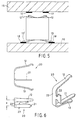
- FIGS. 1 and 5 only the outline of the insulating body 11 and the mutually opposite sides of the insulating body 11 projecting beyond the outline of contact legs 12, 13 and 12 ', 13' are shown in FIGS. 1 and 5.
- These contact legs are under an outwardly directed spring tension, so that they engage between two circuit boards 15 and 16 arranged parallel at a distance 14 in a force-fitting or pressure-locking manner on their associated conductor tracks 17 and 18.
- the two printed circuit boards 15 and 16 which in the functional state have, for example, a clear distance of only 3 mm or less, are held in parallel in a sandwich-like manner by means not shown.
- spacers 19 are shown schematically, due to their tightly flanking the contact strip 10 as a support body, ensure that the contact strip, which is only held in a pressure-locking manner via its contact elements 12, 13, 12 ', 13' between the plates, reliably maintains its intended position with respect to the conductor tracks.
- the contact legs designated by 12 and 13 in FIG. 4 belong to a different contact element than those designated by 12 'and 13'. This is easy to understand on the basis of the illustration in FIG. 6.
- the view shows that a contact element 20 essentially has the shape of the letter E.
- the two outer legs of the E are the contact legs 12 and 13.
- a third, rectilinear leg as the bearing section 21.
- This bearing section 21 is punched out of the same flat sheet of contact metal, in particular beryllium bronze, and is only bent over, as are the contact legs 12 and 13.
- the bearing section 21 is connected to the material strip 23 via a short transition section 22 connected, from which the two legs 12 and 13 are punched out and deformed.
- the bearing section 21 comes into a plane that lies laterally next to the plane of the contact legs 12 and 13, namely by a distance x that corresponds to the grid or pole distance of the contact strip.
- the insulating body 11 is an injection molded component made of a very dimensionally stable material that has practically no shrinkage.
- the insulator has a number of thin webs 24 which are integrally connected to one another by means of core sections 25 which are smaller in outline.
- core sections 25 which are smaller in outline.
- two such core sections 25 lie close together to form a slot 26.
- This slot 26 is thus an insulating body slot into which a contact element 20 with its bearing section 21 is inserted from one of the two possible sides and then held firmly therein.
- this bearing section 21 is located laterally next to the contact sections 12, 13 of the same contact element 20. Consequently, in FIG. 4, the contact element with 20 'arranged in the same plane as the bearing section 21 of the contact element 20 and its contact leg with 12' and 13 ' designated.
- This contact element 20 ' is inserted with its bearing section, which is not visible in FIG. 4, from the other side into the adjacent insertion space.
- This comb-like intermeshing of bearing sections 21 of one contact element 20 between the contact legs 12 'and 13' of the respectively adjacent contact element 20 ' enables a very high packing density or number of poles per unit length to be achieved.
- the contact strip 10 which is shown in FIG. 5, differs from the previously described contact strip 10 essentially only with regard to its contact legs 13 or 13 ', which emerge downwards in the drawing and which are designed as SMT soldering feet aligned parallel to the conductor track 18 are. 5, the upper circuit board 15 is still shown at a distance. In the operational state, however, it is so close to the lower circuit board 16 that the contact legs 12 and 12 'of the relevant contact elements 20 and 20' bear on the conductor tracks 17 under their own spring pressure.
- the tongue-shaped bearing sections 21 are each self-anchored in the insulating body slots 26.
- the tongues 21 have edge edge formations 27 of approximately the type recognizable in FIG. 6, which can claw into the plastic material of the insulating body 10.
- an alternative is also within the scope of the invention, which in turn uses the basic E-shape in the view of a contact element 20, but in which, for example by folding, the bearing section 21 would lie in the same plane as the contact legs 12 and 13 4 shows that it would then also be possible to anchor a contact element in an insulating body slot 26 with its central bearing section. In this case could, should however, the contact elements cannot be connected to the insulating body 11 from different sides.
- contact legs 12 and 13 project freely, because only the central tongue is held on the insulating body. This ensures excellent spring properties and contact forces.
- the contact strip 10 can be made in very small dimensions, for example with grid spacing x of approximately 0.5 mm and for a printed circuit board spacing 14 of less than 3 mm.
Landscapes
- Coupling Device And Connection With Printed Circuit (AREA)
- Multi-Conductor Connections (AREA)
Applications Claiming Priority (2)
| Application Number | Priority Date | Filing Date | Title |
|---|---|---|---|
| DE19617121 | 1996-04-29 | ||
| DE19617121A DE19617121C1 (de) | 1996-04-29 | 1996-04-29 | Kontaktleiste für Leiterplatten |
Publications (3)
| Publication Number | Publication Date |
|---|---|
| EP0805520A2 true EP0805520A2 (fr) | 1997-11-05 |
| EP0805520A3 EP0805520A3 (fr) | 1999-01-13 |
| EP0805520B1 EP0805520B1 (fr) | 2006-10-18 |
Family
ID=7792796
Family Applications (1)
| Application Number | Title | Priority Date | Filing Date |
|---|---|---|---|
| EP97102560A Expired - Lifetime EP0805520B1 (fr) | 1996-04-29 | 1997-02-18 | Connecteur de bords d'une carte à circuits imprimés |
Country Status (4)
| Country | Link |
|---|---|
| US (1) | US5951303A (fr) |
| EP (1) | EP0805520B1 (fr) |
| JP (1) | JP3742937B2 (fr) |
| DE (2) | DE19617121C1 (fr) |
Families Citing this family (11)
| Publication number | Priority date | Publication date | Assignee | Title |
|---|---|---|---|---|
| EP0903810A3 (fr) * | 1997-09-18 | 2000-03-29 | The Whitaker Corporation | Connecteur pour substrats adjacents portant un circuit |
| US6758702B2 (en) | 2000-02-24 | 2004-07-06 | Fci Americas Technology, Inc. | Electrical connector with compression contacts |
| US6488513B1 (en) | 2001-12-13 | 2002-12-03 | Intercon Systems, Inc. | Interposer assembly for soldered electrical connections |
| SG104969A1 (en) * | 2002-05-24 | 2004-07-30 | Fci Asia Technology Pte Ltd | An electrical connector |
| JP4427274B2 (ja) * | 2003-05-28 | 2010-03-03 | 佐鳥エス・テック株式会社 | 電動工具用スイッチ |
| US7455556B2 (en) * | 2003-06-11 | 2008-11-25 | Cinch Connectors, Inc. | Electrical contact |
| US7625216B2 (en) * | 2003-06-11 | 2009-12-01 | Cinch Connectors, Inc. | Electrical connector |
| US6921270B2 (en) * | 2003-06-11 | 2005-07-26 | Cinch Connectors, Inc. | Electrical connector |
| US7435105B2 (en) * | 2004-03-29 | 2008-10-14 | Finisar Corporation | Electrical connector for use in an optical transceiver module |
| JP6821522B2 (ja) * | 2017-06-27 | 2021-01-27 | モレックス エルエルシー | ソケット |
| CN211605463U (zh) * | 2020-01-07 | 2020-09-29 | 番禺得意精密电子工业有限公司 | 电连接器 |
Family Cites Families (7)
| Publication number | Priority date | Publication date | Assignee | Title |
|---|---|---|---|---|
| US4699593A (en) * | 1986-01-14 | 1987-10-13 | Amp Incorporated | Connector having contact modules for a substrate such as an IC chip carrier |
| JP2535766Y2 (ja) * | 1990-12-17 | 1997-05-14 | 日本エー・エム・ピー株式会社 | 基板間相互接続装置 |
| US5125846A (en) * | 1991-07-25 | 1992-06-30 | Molex Incorporated | Input-output electrical connector |
| US5199884A (en) * | 1991-12-02 | 1993-04-06 | Amp Incorporated | Blind mating miniature connector |
| US5358411A (en) * | 1993-08-09 | 1994-10-25 | The Whitaker Corporation | Duplex plated epsilon compliant beam contact and interposer |
| KR950033507A (ko) * | 1994-02-08 | 1995-12-26 | 오가 노리오 | Ic 측정시험장치 및 이것을 사용한 ic 측정시험방법 |
| US5484295A (en) * | 1994-04-01 | 1996-01-16 | Teledyne Electronic Technologies | Low profile compression electrical connector |
-
1996
- 1996-04-29 DE DE19617121A patent/DE19617121C1/de not_active Expired - Fee Related
-
1997
- 1997-02-18 EP EP97102560A patent/EP0805520B1/fr not_active Expired - Lifetime
- 1997-02-18 DE DE59712749T patent/DE59712749D1/de not_active Expired - Fee Related
- 1997-04-10 JP JP12616297A patent/JP3742937B2/ja not_active Expired - Fee Related
- 1997-04-28 US US08/847,846 patent/US5951303A/en not_active Expired - Fee Related
Also Published As
| Publication number | Publication date |
|---|---|
| EP0805520B1 (fr) | 2006-10-18 |
| DE19617121C1 (de) | 1997-07-24 |
| US5951303A (en) | 1999-09-14 |
| JPH1050432A (ja) | 1998-02-20 |
| JP3742937B2 (ja) | 2006-02-08 |
| EP0805520A3 (fr) | 1999-01-13 |
| DE59712749D1 (de) | 2006-11-30 |
Similar Documents
| Publication | Publication Date | Title |
|---|---|---|
| DE69419406T2 (de) | Elektrischer verbinder zum verbinden von einer elektronischen speicherkarte | |
| EP1253670B1 (fr) | Borne à ressort et barette à bornes | |
| DE3522708C2 (fr) | ||
| DE1790342A1 (de) | Federkontaktteil | |
| DE2460704A1 (de) | Elektrischer kontakt | |
| DE2204924A1 (de) | Elektrische Verbinderanordnung | |
| DE10006530A1 (de) | Antennenfeder | |
| DE2234961C3 (de) | Verfahren zur Herstellung von Steckern für Schaltplatten | |
| DE102016116510A1 (de) | Leiteranschlussklemme | |
| DE4243076A1 (de) | Kotaktiereinrichtung für eine Chipkarte | |
| DE3590369C2 (fr) | ||
| EP0805520B1 (fr) | Connecteur de bords d'une carte à circuits imprimés | |
| DE19755715A1 (de) | Chipkartenleser | |
| DE2659645C2 (fr) | ||
| EP0129068A1 (fr) | Relais électromagnétique miniaturisé et méthode de fabrication | |
| DE3447135A1 (de) | Schraubenlose anschluss- und verbindungsklemme fuer elektrische leitungen | |
| DE2345583C3 (de) | Steckerleiste | |
| DE69506750T2 (de) | Ebene Schaltungsplatte | |
| DE19706636C2 (de) | Elektrische Anschlußvorrichtung für in einer Reihe angeordnete Verbraucher, insbesondere Magnetventile | |
| DE3855949T2 (de) | Gehäuse für integrierte Schaltungen | |
| DE19833248C2 (de) | Vorrichtung zum Führen und Massekontaktieren von Leiterplatten | |
| DE29607758U1 (de) | Kontaktleiste für Leiterplatten | |
| EP1182735A2 (fr) | Réglette d'interconnexion électrique | |
| DE29720511U1 (de) | Einbaugehäuse für Leiterplatten und Elektronikbausteine | |
| DE19630859C2 (de) | Reihenklemme, insbesondere Initiator-Aktor-Klemme |
Legal Events
| Date | Code | Title | Description |
|---|---|---|---|
| PUAI | Public reference made under article 153(3) epc to a published international application that has entered the european phase |
Free format text: ORIGINAL CODE: 0009012 |
|
| AK | Designated contracting states |
Kind code of ref document: A2 Designated state(s): DE FI FR GB IT NL SE |
|
| PUAL | Search report despatched |
Free format text: ORIGINAL CODE: 0009013 |
|
| AK | Designated contracting states |
Kind code of ref document: A3 Designated state(s): DE FI FR GB IT NL SE |
|
| 17P | Request for examination filed |
Effective date: 19981222 |
|
| RAP1 | Party data changed (applicant data changed or rights of an application transferred) |
Owner name: LUMBERG CONNECT GMBH & CO. KG |
|
| GRAP | Despatch of communication of intention to grant a patent |
Free format text: ORIGINAL CODE: EPIDOSNIGR1 |
|
| RIC1 | Information provided on ipc code assigned before grant |
Ipc: H01R 12/22 20060101ALI20060531BHEP Ipc: H01R 12/04 20060101AFI20060531BHEP |
|
| GRAS | Grant fee paid |
Free format text: ORIGINAL CODE: EPIDOSNIGR3 |
|
| GRAA | (expected) grant |
Free format text: ORIGINAL CODE: 0009210 |
|
| AK | Designated contracting states |
Kind code of ref document: B1 Designated state(s): DE FI FR GB IT NL SE |
|
| PG25 | Lapsed in a contracting state [announced via postgrant information from national office to epo] |
Ref country code: IT Free format text: LAPSE BECAUSE OF FAILURE TO SUBMIT A TRANSLATION OF THE DESCRIPTION OR TO PAY THE FEE WITHIN THE PRESCRIBED TIME-LIMIT;WARNING: LAPSES OF ITALIAN PATENTS WITH EFFECTIVE DATE BEFORE 2007 MAY HAVE OCCURRED AT ANY TIME BEFORE 2007. THE CORRECT EFFECTIVE DATE MAY BE DIFFERENT FROM THE ONE RECORDED. Effective date: 20061018 |
|
| REG | Reference to a national code |
Ref country code: GB Ref legal event code: FG4D Free format text: NOT ENGLISH |
|
| REF | Corresponds to: |
Ref document number: 59712749 Country of ref document: DE Date of ref document: 20061130 Kind code of ref document: P |
|
| GBT | Gb: translation of ep patent filed (gb section 77(6)(a)/1977) |
Effective date: 20061221 |
|
| REG | Reference to a national code |
Ref country code: SE Ref legal event code: TRGR |
|
| ET | Fr: translation filed | ||
| PLBE | No opposition filed within time limit |
Free format text: ORIGINAL CODE: 0009261 |
|
| STAA | Information on the status of an ep patent application or granted ep patent |
Free format text: STATUS: NO OPPOSITION FILED WITHIN TIME LIMIT |
|
| 26N | No opposition filed |
Effective date: 20070719 |
|
| PGFP | Annual fee paid to national office [announced via postgrant information from national office to epo] |
Ref country code: FI Payment date: 20080213 Year of fee payment: 12 Ref country code: SE Payment date: 20080213 Year of fee payment: 12 Ref country code: NL Payment date: 20080229 Year of fee payment: 12 Ref country code: IT Payment date: 20080228 Year of fee payment: 12 Ref country code: GB Payment date: 20080204 Year of fee payment: 12 |
|
| PGFP | Annual fee paid to national office [announced via postgrant information from national office to epo] |
Ref country code: FR Payment date: 20080226 Year of fee payment: 12 Ref country code: DE Payment date: 20080423 Year of fee payment: 12 |
|
| EUG | Se: european patent has lapsed | ||
| GBPC | Gb: european patent ceased through non-payment of renewal fee |
Effective date: 20090218 |
|
| PG25 | Lapsed in a contracting state [announced via postgrant information from national office to epo] |
Ref country code: FI Free format text: LAPSE BECAUSE OF NON-PAYMENT OF DUE FEES Effective date: 20090218 |
|
| NLV4 | Nl: lapsed or anulled due to non-payment of the annual fee |
Effective date: 20090901 |
|
| REG | Reference to a national code |
Ref country code: FR Ref legal event code: ST Effective date: 20091030 |
|
| PG25 | Lapsed in a contracting state [announced via postgrant information from national office to epo] |
Ref country code: NL Free format text: LAPSE BECAUSE OF NON-PAYMENT OF DUE FEES Effective date: 20090901 |
|
| PG25 | Lapsed in a contracting state [announced via postgrant information from national office to epo] |
Ref country code: DE Free format text: LAPSE BECAUSE OF NON-PAYMENT OF DUE FEES Effective date: 20090901 |
|
| PG25 | Lapsed in a contracting state [announced via postgrant information from national office to epo] |
Ref country code: GB Free format text: LAPSE BECAUSE OF NON-PAYMENT OF DUE FEES Effective date: 20090218 Ref country code: FR Free format text: LAPSE BECAUSE OF NON-PAYMENT OF DUE FEES Effective date: 20090302 |
|
| PG25 | Lapsed in a contracting state [announced via postgrant information from national office to epo] |
Ref country code: IT Free format text: LAPSE BECAUSE OF NON-PAYMENT OF DUE FEES Effective date: 20090218 |
|
| PG25 | Lapsed in a contracting state [announced via postgrant information from national office to epo] |
Ref country code: SE Free format text: LAPSE BECAUSE OF NON-PAYMENT OF DUE FEES Effective date: 20090219 |