EP0805527B1 - Module laser à diode de haute efficacité - Google Patents
Module laser à diode de haute efficacité Download PDFInfo
- Publication number
- EP0805527B1 EP0805527B1 EP97106741A EP97106741A EP0805527B1 EP 0805527 B1 EP0805527 B1 EP 0805527B1 EP 97106741 A EP97106741 A EP 97106741A EP 97106741 A EP97106741 A EP 97106741A EP 0805527 B1 EP0805527 B1 EP 0805527B1
- Authority
- EP
- European Patent Office
- Prior art keywords
- laser diode
- heat sink
- height
- lid
- diode package
- Prior art date
- Legal status (The legal status is an assumption and is not a legal conclusion. Google has not performed a legal analysis and makes no representation as to the accuracy of the status listed.)
- Expired - Lifetime
Links
Images

Classifications
-
- H—ELECTRICITY
- H01—ELECTRIC ELEMENTS
- H01S—DEVICES USING THE PROCESS OF LIGHT AMPLIFICATION BY STIMULATED EMISSION OF RADIATION [LASER] TO AMPLIFY OR GENERATE LIGHT; DEVICES USING STIMULATED EMISSION OF ELECTROMAGNETIC RADIATION IN WAVE RANGES OTHER THAN OPTICAL
- H01S5/00—Semiconductor lasers
- H01S5/40—Arrangement of two or more semiconductor lasers, not provided for in groups H01S5/02 - H01S5/30
- H01S5/4025—Array arrangements, e.g. constituted by discrete laser diodes or laser bar
- H01S5/4031—Edge-emitting structures
- H01S5/4043—Edge-emitting structures with vertically stacked active layers
- H01S5/405—Two-dimensional arrays
-
- H—ELECTRICITY
- H01—ELECTRIC ELEMENTS
- H01S—DEVICES USING THE PROCESS OF LIGHT AMPLIFICATION BY STIMULATED EMISSION OF RADIATION [LASER] TO AMPLIFY OR GENERATE LIGHT; DEVICES USING STIMULATED EMISSION OF ELECTROMAGNETIC RADIATION IN WAVE RANGES OTHER THAN OPTICAL
- H01S5/00—Semiconductor lasers
- H01S5/02—Structural details or components not essential to laser action
- H01S5/022—Mountings; Housings
- H01S5/0233—Mounting configuration of laser chips
-
- H—ELECTRICITY
- H01—ELECTRIC ELEMENTS
- H01S—DEVICES USING THE PROCESS OF LIGHT AMPLIFICATION BY STIMULATED EMISSION OF RADIATION [LASER] TO AMPLIFY OR GENERATE LIGHT; DEVICES USING STIMULATED EMISSION OF ELECTROMAGNETIC RADIATION IN WAVE RANGES OTHER THAN OPTICAL
- H01S5/00—Semiconductor lasers
- H01S5/02—Structural details or components not essential to laser action
- H01S5/024—Arrangements for thermal management
- H01S5/02476—Heat spreaders, i.e. improving heat flow between laser chip and heat dissipating elements
-
- H—ELECTRICITY
- H01—ELECTRIC ELEMENTS
- H01S—DEVICES USING THE PROCESS OF LIGHT AMPLIFICATION BY STIMULATED EMISSION OF RADIATION [LASER] TO AMPLIFY OR GENERATE LIGHT; DEVICES USING STIMULATED EMISSION OF ELECTROMAGNETIC RADIATION IN WAVE RANGES OTHER THAN OPTICAL
- H01S5/00—Semiconductor lasers
- H01S5/02—Structural details or components not essential to laser action
- H01S5/022—Mountings; Housings
- H01S5/023—Mount members, e.g. sub-mount members
-
- H—ELECTRICITY
- H01—ELECTRIC ELEMENTS
- H01S—DEVICES USING THE PROCESS OF LIGHT AMPLIFICATION BY STIMULATED EMISSION OF RADIATION [LASER] TO AMPLIFY OR GENERATE LIGHT; DEVICES USING STIMULATED EMISSION OF ELECTROMAGNETIC RADIATION IN WAVE RANGES OTHER THAN OPTICAL
- H01S5/00—Semiconductor lasers
- H01S5/02—Structural details or components not essential to laser action
- H01S5/022—Mountings; Housings
- H01S5/0235—Method for mounting laser chips
- H01S5/02355—Fixing laser chips on mounts
- H01S5/0237—Fixing laser chips on mounts by soldering
-
- H—ELECTRICITY
- H01—ELECTRIC ELEMENTS
- H01S—DEVICES USING THE PROCESS OF LIGHT AMPLIFICATION BY STIMULATED EMISSION OF RADIATION [LASER] TO AMPLIFY OR GENERATE LIGHT; DEVICES USING STIMULATED EMISSION OF ELECTROMAGNETIC RADIATION IN WAVE RANGES OTHER THAN OPTICAL
- H01S5/00—Semiconductor lasers
- H01S5/02—Structural details or components not essential to laser action
- H01S5/024—Arrangements for thermal management
- H01S5/02469—Passive cooling, e.g. where heat is removed by the housing as a whole or by a heat pipe without any active cooling element like a TEC
-
- H—ELECTRICITY
- H01—ELECTRIC ELEMENTS
- H01S—DEVICES USING THE PROCESS OF LIGHT AMPLIFICATION BY STIMULATED EMISSION OF RADIATION [LASER] TO AMPLIFY OR GENERATE LIGHT; DEVICES USING STIMULATED EMISSION OF ELECTROMAGNETIC RADIATION IN WAVE RANGES OTHER THAN OPTICAL
- H01S5/00—Semiconductor lasers
- H01S5/40—Arrangement of two or more semiconductor lasers, not provided for in groups H01S5/02 - H01S5/30
- H01S5/4018—Lasers electrically in series
-
- H—ELECTRICITY
- H01—ELECTRIC ELEMENTS
- H01S—DEVICES USING THE PROCESS OF LIGHT AMPLIFICATION BY STIMULATED EMISSION OF RADIATION [LASER] TO AMPLIFY OR GENERATE LIGHT; DEVICES USING STIMULATED EMISSION OF ELECTROMAGNETIC RADIATION IN WAVE RANGES OTHER THAN OPTICAL
- H01S5/00—Semiconductor lasers
- H01S5/40—Arrangement of two or more semiconductor lasers, not provided for in groups H01S5/02 - H01S5/30
- H01S5/4025—Array arrangements, e.g. constituted by discrete laser diodes or laser bar
-
- Y—GENERAL TAGGING OF NEW TECHNOLOGICAL DEVELOPMENTS; GENERAL TAGGING OF CROSS-SECTIONAL TECHNOLOGIES SPANNING OVER SEVERAL SECTIONS OF THE IPC; TECHNICAL SUBJECTS COVERED BY FORMER USPC CROSS-REFERENCE ART COLLECTIONS [XRACs] AND DIGESTS
- Y10—TECHNICAL SUBJECTS COVERED BY FORMER USPC
- Y10S—TECHNICAL SUBJECTS COVERED BY FORMER USPC CROSS-REFERENCE ART COLLECTIONS [XRACs] AND DIGESTS
- Y10S257/00—Active solid-state devices, e.g. transistors, solid-state diodes
- Y10S257/91—Diode arrays, e.g. diode read-only memory array
Definitions
- the present invention relates generally to lasers diodes and, in particular, to a package for a laser diode that reduces the thermal resistance between the junction of the laser diode and the ultimate thermal reservoir.
- Semiconductor laser diodes have numerous advantages. They are small in that the widths of their active regions are typically submicron to a few microns and their heights are usually no more than a fraction of a millimeter. The length of their active regions is typically less than about a millimeter.
- the internal reflective surfaces, which are required in order to produce emission in one direction, are formed by cleaving the substrate from which the laser diodes are produced and, thus, have high mechanical stability.
- semiconductor laser diodes with pulsed junction laser diodes having external quantum efficiencies near 50% in some cases.
- Semiconductor lasers produce radiation at wavelengths from about 20 to about 0.7 microns depending on the choice of semiconductor alloy.
- laser diodes made of gallium arsenide with aluminum doping (AlGaAs) emit radiation at approximately 0.8 microns ( ⁇ 800 nm) which is near the absorption spectrum of common solid state laser rods and slabs made from Neodymium doped, Yttrium-Aluminum Garnet (Nd:YAG), and other crystals and glasses.
- AlGaAs gallium arsenide with aluminum doping
- semiconductor laser diodes can be used as the optical pumping source for larger, solid state laser systems.
- the emitted wavelength of a laser diode is a function of its junction temperature.
- maintaining a constant junction temperature is essential.
- AlGaAs laser diodes used to pump a Nd:YAG rod or slab should emit radiation at 808 nm since this is the wavelength at which optimum absorption exists in the Nd:YAG.
- the wavelength shifts 1 nm.
- controlling the junction temperature and, thus, properly dissipating the heat is critical.
- One known package which attempts to resolve these thermally-related problems includes the use of a thin, thermally conductive ceramic structure, like beryllium oxide, which is bonded to a thermal reservoir.
- the ceramic structure includes straight grooves cut therein in which the individual laser diodes are placed.
- a metallized layer extends from groove to groove to conduct electricity therethrough and supply electrical power to each of the plurality of laser diodes.
- the laser diodes are soldered in the grooves to the metallized layer.
- laser diodes typically have a slight curvature due to the process by which they are made. Placing a curved laser diode in the straight groove of this known package results in additional stress on the laser diode and an uneven solder bond along the length of the laser diode which can lead to failure. Also, the bottom side of the laser diode in the groove, which is the reflective surface, cannot be cleaned after it is installed which may lead to failures. Additionally, most ceramics, even beryllium oxide, have a lower thermal conductivity than conductive metals such as copper or silver. If beryllium oxide is used, further problems arise since it is a toxic material and cutting grooves produces airborne dust particles.
- Patent Abstracts of Japan, vol. 010, no. 061 (E-387), 11 March 1986 (ESR: A doc) discloses a laser diode package according to the preamble of claim 1.
- a laser diode package includes a laser diode, a heat sink and a lid.
- the laser diode has an emitting surface, a reflective surface opposing the emitting surface, and first and second side surfaces between the emitting surface and the reflective surface.
- the laser diode has a diode height defined between the emitting surface and the reflective surface.
- the heat sink has an interior surface, an exterior surface opposing the interior surface, a top surface and a base surface.
- the height of the heat sink is defined between the top surface and the base surface and is less than approximately four times the laser diode height.
- the first surface of the diode is attached to the interior surface of the heat sink with a first solder layer.
- the base surface of the heat sink is coupled to a thermal reservoir.
- the lid is attached to the second surface of the laser diode via a second solder layer.
- An upper end of the lid is near the emitting surface of the laser diode.
- a lower end of the lid is typically slightly below the reflecting surface of the laser diode.
- a region below the reflective surface between the interior surface of the heat sink and the lid is filled with an inert gas, usually air.
- the heat sink and lid are typically made from an electrically conductive material.
- electrical power is applied to the laser diode package, electromagnetic radiation if produced at the junction of the laser diode and emitted at the emitting surface. Also, a substantial amount of heat is produced. Because of the minimal height of the heat sink, the laser diode package has a minimal thermal resistance between the junction and the thermal reservoir to which the base surface is coupled. Consequently, the junction temperature is minimized.
- the laser diode package of the present invention exposes more of the laser diode, especially at its reflective surface, than known packages which facilitates cleaning after the laser diode has been soldered into the package. Also, the laser diode package provides for structural integrity to the laser diode during handling and transportation. And, the package provides easy testing of the laser diode prior to assembly into an array.
- a plurality of laser diode packages are grouped together to form an array.
- the heat sink of each of the laser diode packages is attached to a backplane which is then connected to a thermal reservoir.
- the heat sink of each laser diode package may be soldered to an electrically insulative backplane, or attached to an electrically conductive backplane via electrically nonconductive, but thermally conductive materials such as thermal epoxies.
- the exterior surface of each heat sink is provided with a groove to receive solder to join that heat sink with an adjacent lid.
- a laser diode package 10 is illustrated in an end view.
- the laser diode package 10 includes a laser diode 12, a heat sink 14, and a lid 17.
- the laser diode 12 is illustrated as emitting photons which are depicted as arrows. As illustrated best in FIG. 1, the laser diode 12 is "sandwiched" between the heat sink 14 and the lid 17.
- the laser diode 12 includes an emitting surface 20 from which the photons are emitted and a reflective surface 22 positioned opposite the emitting surface 20.
- the height of the laser diode 12 is defined as the distance between the emitting surface 20 and the reflecting surface 22.
- the junction of the laser diode 12 where the photons are produced is nearest the heat sink 14 in the laser diode package 10. Electrical power is guided to defined regions of the junction by providing electrically conductive material in the laser diode 12 adjacent those regions and less electrically conductive material outside those regions. Consequently, the laser diode 12 has a plurality of emission points 24 (FIG. 4) on the emitting surface 22 corresponding to those regions where electrical energy is converted into light energy. When the electrical power is applied, photons propagate though the junction and are reflected off the reflecting surface 22 such that emission only occurs at the emitting surface 20.
- the laser diode 12 further includes a first surface 26 and a second surface 28 to which the heat sink 14 and the lid 17 are soldered.
- a first solder layer 30 attaches the first surface 26 of the laser diode 12 to the heat sink 14.
- a second solder layer 32 attaches the second surface 28 of the laser diode 12 to the lid 17.
- the solders used in the first and second solder layers 30 and 32 are the same, although they may be different.
- Common solders used at the first and second solder layers 30 and 32 include various materials having indium including pure indium, indium gallium alloys, indium tin alloys, and indium gallium tin alloys. In a preferred embodiment, pure indium is used and deposited by thermal evaporation techniques.
- the thickness of the first and second solder layers 30 and 32 is in the range from about 1 micron to about 5 microns.
- the lid 17 has an upper end surface 40 near the emitting surface 20 of the laser diode 12 and a lower end surface 42 that at least extends beyond the reflective surface 22 of the laser diode 12.
- the height of the lid 17 defined between the upper end surface 40 and the lower end surface 42 is at least slightly larger than the height of the laser diode 12.
- the lid 17 includes an inner surface 44 to which the second solder layer 32 is attached and an outer surface 46 facing outwardly.
- the heat sink 14 has a top surface 50 and a base surface 52.
- the height of the heat sink 14 is defined as the distance between the top surface 50 and the base surface 52.
- the base surface 52 is the surface to which the laser diode package 10 attaches, directly or indirectly, to a thermal reservoir where the heat produced at the junction of the laser diode 12 is dissipated as described below in reference to FIG. 5.
- the heat sink 14 further includes an interior surface 54 to which the first solder layer 30 is attached, and an exterior surface 56 opposing the interior surface 54.
- the height of the heat sink 14 is typically less than approximately four times the height of the laser diode 12.
- the laser diode 12 has a height approximately 0.02 inch (0.5 mm) and the heat sink 14 has a height less than 0.08 inch (2.0 mm).
- the height of the heat sink 14 is less than approximately two times the height of the laser diode 12.
- the thickness of the heat sink 14, measured between the interior surface 54 and exterior surface 56, is generally greater than the thickness of the laser diode 12 which is measured between its first and second surfaces 26 and 28.
- the heat sink 14 is approximately 0.007 inch (0.18 mm) thick and the laser diode 12 has a thickness of approximately 0.005 inch (0.13 mm).
- the thickness of the heat sink 14 is more than about 10% of its height. The thicker the heat sink 14 is, the less thermal resistance the heat sink 14 has because the cross-sectional area through which the heat flows is increased. Increasing the thickness of the heat sink 14, however, reduces the packing density of an array of laser diode packages 10.
- the lid 17 Because the purpose of the lid 17 is primarily to provide structural integrity and a low resistance electrical contact to the laser diode 12 and not remove heat, the lid 17 has a lesser thickness than the laser diode 12 and does not need to be coupled to the thermal reservoir. Thus, the lid 17 generally has a height that is slightly longer than the height of the laser diode 12 and a thickness that is generally less than the laser diode 12. In one embodiment, the thickness of the lid 17 is approximately 0.002 inch (0.05 mm) and its height is about 0.025 inch ( ⁇ 0.6 mm).
- the laser diode package 10 minimizes the likelihood of electrical shorts between the heat sink 14 and the lid 17 because the lid 17 does not have a significant height and, therefore, a significant area to which arcing may occur.
- the gap between the heat sink 14 on its interior side 54 below the reflective surface 22 of the laser diode 12 and the lid 17 is filled with inert gas, usually air. If the lid 17 and the heat sink 14 are made of flexible thin foils, there is a chance that the two pieces will bend and contact each other which leads to an electrical short. Thus, the short heights on the lid 17 and the heat sink 14, as have been described thus far, are preferred.
- the heights of the lid 17 and the heat sink 14 are also configured to allow the access to the reflective surface 22 of the laser diode 12 for cleaning that surface 22 after assembly. If the lid 17 and the heat sink 14 are made of flexible thin foils, then having a substantial height will likely lead to one or both of the pieces covering the reflective surface 22. Consequently, short heights in the lid 17 and the heat sink 14 are also preferable for this reason as well.
- the lid 17 may have a height that is approximately the height of the heat sink 14.
- the lower end 42 of the lid 17 may be bonded to a thermal reservoir as is the heat sink 14 and remove a portion of the heat produced by the laser diode 12.
- the removal of heat through the lid 17 is not as effective as the removal of heat through the heat sink 14.
- the length of the heat sink 14 and the lid 17, shown in FIGS. 2-4, is a function of the length of the laser diode 12.
- the laser diode 12 has a length of approximately 1 cm, although variations exist which depend on the process by which the laser diode 12 is produced, and also by the application.
- the overall thermal resistance between the junction of the laser diode 12 and the thermal reservoir is largely dependent on the thermal conductivity of the material used in the heat sink 14.
- the electrical current must flow from the heat sink 14, through the laser diode 12, and into the lid 17 for the junction of the laser diode 12 to convert electrical energy to radiative energy.
- the material of the heat sink 14 generally has a high thermal conductivity and is typically electrically conductive like copper, silver, or gold. Based on the relatively small thickness of the heat sink 14, the material of the heat sink 14 is supplied in the form of foil. It is then cut or etched into the shape of the heat sink 14.
- the heat sink 14 may be made of a non-metallic material, such as diamond, boron nitride, aluminum nitride, or beryllium oxide, which have a high thermal conductivity.
- a heat sink 14 would require an electrically conductive metallized layer to provide a path through which the electrical current may flow.
- the metallized layer would be on the interior surface 54 of the heat sink 14 near the laser diode 12, on the top surface 50, and on at least a portion of the exterior surface 56.
- the material of the lid 17 is less critical to the thermal performance of the laser diode package 10 than the material of the heat sink 14.
- the lid 17 is made of copper.
- the heat sink 14 may include a groove 60 extending along at least a substantial portion of the length of the heat sink 14 on its exterior surface 56 adjacent the top surface 50.
- the attachment of adjacent laser diode packages 10 is illustrated in more detail in FIG. 5.
- the groove 60 typically extends into the heat sink 14 for a distance equal to approximately half of the thickness of the heat sink 14.
- the height of the grooves 60 is generally less than the height of the laser diode 12.
- solder is placed within the groove 60 such that the heat sink 14 is made integral with the lid 17 of the adjacent laser diode package 10.
- the solder placed into the groove 60 is different than the solder placed in the first and second solder layers 30 and 32 which attach the laser diode 12 to the heat sink 14 and lid 17, respectively. If the same solders were used, then the temperatures required to flow the solder in the groove 60 would likely cause the solder to reflow in the first and second solder layers 30 and 32 near the laser diode 12 such that the laser diode package 10 may become unassembled. Consequently, the solder chosen for the groove 60 has a melting temperature that is less than the melting temperature of the solder chosen in the first and second solder layers 30 and 32.
- the laser diode package 10 has several distinct advantages other than the enhanced thermal performance associated with its geometry. Once the laser diode package 10 is assembled, the reflective surface 22 of the laser diode 12 can be accessed for cleaning which is typically accomplished by the use of solvents. Applying the solvents is easy since there are no structures obstructing their direct application to the reflective surface 22 due to the geometrical configuration of the lid 17 and heat sink 14. Cleaning of the reflective surface 22 ensures than no solder or solder flux is present on the reflective surface 22 which may cause radiation to be absorbed and not reflected. Absorbed radiation creates high local temperatures that can lead to a catastrophic failure of the laser diode 12.
- the relative flexibility of the lid 17 and heat sink 14 accommodates the inherent curvature that is present in the laser diode 12. This inherent curvature is due to the process by which the laser diode 12 is produced which involves the deposit of several layers of material on a substrate. The layers, which include materials having various coefficients of thermal expansion, are deposited at elevated temperatures. Once the layers have cooled and the substrate is cut, or cleaved, to produce the individual diode bars 12, the mismatch of coefficients of thermal expansion leads to the bending, or bowing, of the individual laser diodes 12. Because the lid 17 and the heat sink 14 are typically less than 0.010 inch thick and made of metal, they are flexible and, in essence, conform to the curvature of the laser diode 12.
- the first and second solder layers 30 and 32 can have a constant thickness along the entire length of the laser diode 12. This is important to ensure that the electrical resistance of the laser diode package 10, which is largely a function of the solder material used at the first and second soldering layers 30 and 32, remains constant throughout the length of the laser diode 12. If the electrical resistance is not constant, then the flux of electrical current may be extremely large in the regions of less electrical resistance which can cause an uneven distribution of radiation from the laser diode 12.
- the laser diode package 10 can also be tested in an easy manner before it is further assembled into an array. Testing is necessary to characterize the laser diode 12 and ensure that each laser diode 12 placed into an array will perform adequately. For example, the threshold current is measured to determine the input current required before radiation is produced. The output power of the laser diode 12 is another parameter which is useful to know before placing the laser diode 12 in an array. The threshold current and the output power are used to determine the efficiency of the laser diode 12. Also, the wavelength emitted from each laser diode 12 is not exactly the same and must be determined.
- the thermal capacity of the heat sink 14, determined by the specific heat and the density of the material of the heat sink 14, is enough to allow for low power testing of the laser diode package 10 (i.e. a few watts for a few milliseconds).
- the overall cost of packaging the laser diode 12 is relatively inexpensive. And, these materials are not hazardous or toxic which minimizes assembly costs since less precautions are necessary.
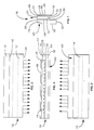
- FIG. 5 illustrates a laser diode array 100 having a plurality of laser diode packages 10 which are arranged in a substantially parallel configuration.
- the plurality of laser diodes packages 10 includes a first end one 10a and a second end one 10b.
- First and second end caps 102 and 104, to which first and second electrical lines 106 and 108 are attached, are at either end of the laser diode array 100.
- the end caps 102 and 104 are made of an electrically conductive material, usually copper. Electrical current conducts from the first electrical line 106, through the first end cap 102, through the plurality of laser diode packages 10, into the second end cap 104, and out the second electrical line 108.
- the grooves 60 are filled with a solder which joins the heat sink 14 of one package 10 to a lid 17 of an adjacent package 10.
- the groove 60 of the first end one 10b of the packages 10 is filled with solder to attach that heat sink 14 to the first end cap 102.
- the solder within the grooves 60 assists in the conduction of electricity between each package 10.
- the packages 10 can lack these grooves 60 and conduct electricity through the packages 10 if adequate contact pressure exists between the heat sink 14 of one package 10 and the lid 17 of an adjacent package 10.
- the lids 17 may include grooves or notches for receiving solder. This may be in addition to, or independent of, the grooves 60 that have been described thus far.
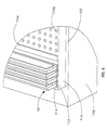
- the heat sink 14 of each of the laser diode packages 10 is bonded to a backplane 110 which is further attached to a thermal reservoir 120 that completes the entire assembly.
- the backplane 110 is attached to the thermal reservoir 120 by a layer 122 which can be a solder joint or thermally conductive epoxies.
- the thermal reservoir 120 is typically a heat exchanger having internal fins through which a fluid is circulated. Consequently, the thermal reservoir 120 is typically a conductive metal, such as copper.
- the backplane 110 is typically made of an electrically nonconductive material and thermally conductive material such as beryllium oxide, boron nitride, aluminum nitride, or diamond. If the material is electrically nonconductive, the electrical power can not flow therethrough (i.e. short) and bypass the laser diode packages 10.
- the base surface 52 of each heat sink 14 is soldered to metallized strips 112 on the backplane 110.
- the solder layer 114 has a thickness that is in the range from about 1 micron to about 0.002 inch and a width that covers at least the thickness of the heat sink 14.
- the solder layers 114 and metallized strips 112 are also present between each of the end caps 102 and 104, and the backplane 110. However, these end caps 102 and 104 can be bonded to the backplane 110 with other materials as well, such as epoxies.
- the backplane 110 can be electrically and thermally conductive (e.g. copper) as long as adequate protection is made to electrically insulate the heat sinks 14 from the backplane 110. This can be accomplished by vacating any solder bonds between those structures and replacing them with electrically insulative materials like epoxies.
- the epoxy is a thermally conductive epoxy like metal-filled epoxy or diamond-filled epoxy.
- the backplane 110 can be coated with a thin dielectric such as silicon oxide prior to the epoxy being applied thereto. A layer of this dielectric with a thickness greater than 0.5 micron provides adequate electrical insulation.
- the backplane 110 is eliminated and the packages 10 are bonded directly to the upper surface of the thermal reservoir 120 which acts as the backplane 120. If the thermal reservoir 120 is metallic, then the electrically insulative measures described in the previous paragraph are incorporated. If the thermal reservoir 120 is electrically non-conductive and made of the materials described above with reference to the electrically non-conductive backplane 110, then the heat sinks 14 can be soldered to the thermal reservoir 120 as they are shown in FIG. 5 soldered to the backplane 110.
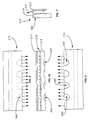
- FIG. 6 illustrates the process by which the laser diode packages 10 are soldered to the backplane 110 on the strips 112.
- the strips 112 can be one continuous stripe 112a.
- the strip 112 can be a series of discontinuous pads 112b.
- the discontinuous pads 112b can be in a variety of shapes including circular (as shown) or rectangular
- FIGS. 7-10 illustrate a laser diode package 210 that is very similar to the package 10 in FIGS. 1-4.
- the only difference is the fact that groove 60 in FIGS. 1-4 is now replaced by a series of notches 260.
- the series of notches 260 serve the same purpose as the groove 60 in that they join (i.e. make integral) a heat sink 214 of one package 210 to a lid 217 of an adjacent package 210.
- the notches 260 are generally uniformly-spaced along the length of the heat sink 214.
- the height of the notches 260 is typically less than the height of the laser diode 212.
- the notches 260 typically extend into the heat sink 214 for a distance equal to approximately half of the thickness of the heat sink 214.
Landscapes
- Physics & Mathematics (AREA)
- Condensed Matter Physics & Semiconductors (AREA)
- General Physics & Mathematics (AREA)
- Electromagnetism (AREA)
- Optics & Photonics (AREA)
- Semiconductor Lasers (AREA)
Claims (34)
- Module de diode laser (10), comprenant:caractérisé en ce queune diode laser (12) ayant une surface d'émission (20), une surface de réflexion (22) opposée à ladite surface d'émission, et des première (26) et deuxième (28) surfaces comprises entre ladite surface d'émission et ladite surface de réflexion, ladite diode laser ayant une hauteur de diode définie entre ladite surface d'émission (20) et ladite surface de réflexion (22);un radiateur (14) soudé à ladite première surface (26) de ladite diode laser (12), ledit radiateur (14) ayant une surface supérieure (50) et une surface de base (52), ladite surface de base devant être couplée à un accumulateur de chaleur (120) pour dissiper la chaleur provenant de ladite diode laser, etun couvercle (17) soudé à ladite deuxième surface (28) de ladite diode laser (12),
la hauteur de radiateur est approximativement inférieure à quatre fois ladite hauteur de diode, ladite hauteur de radiateur étant définie entre ladite surface supérieure (50) et ladite surface de base (52) - Module de diode laser selon la revendication 1, dans lequel ledit couvercle est un deuxième radiateur fixé à ladite deuxième surface de ladite diode laser, ledit radiateur et ledit deuxième radiateur étant de même hauteur qui est approximativement inférieure à quatre fois ladite hauteur de diode.
- Module de diode laser selon la revendication 2, dans lequel les hauteurs dudit radiateur et dudit deuxième radiateur sont configurées pour permettre l'accès à ladite surface de réflexion afin de nettoyer ladite surface de réflexion après que ledit radiateur et ledit deuxième radiateur ont été fixés à ladite diode laser.
- Module de diode laser selon la revendication 1, dans lequel ledit radiateur possède une surface intérieure (54), une surface extérieure (56) opposée à ladite surface intérieure, ladite surface supérieure et ladite surface de base, ladite première surface de ladite diode laser étant fixée avec une première soudure (30) à ladite surface intérieure dudit radiateur, et ledit couvercle étant fixé à ladite deuxième surface de ladite diode laser grâce à une deuxième soudure (32).
- Module de diode laser selon la revendication 3, dans lequel ladite surface de base est une surface de base devant être couplée à un accumulateur de chaleur pour dissiper la chaleur provenant de ladite diode laser de telle manière que ledit module se tienne droit pendant le fonctionnement par rapport audit accumulateur de chaleur, ladite chaleur provenant de ladite diode laser étant transférée par l'intermédiaire dudit radiateur à ladite surface de base et à l'intérieur de l'accumulateur de chaleur.
- Module de diode laser selon la revendication 1, dans lequel ladite surface de réflexion de ladite diode laser est laissée découverte sans obstacle entre ledit radiateur et ledit couvercle pour permettre un nettoyage de ladite surface de réflexion après assemblage.
- Module de diode laser selon la revendication 1 ou 6, dans lequel ledit couvercle possède une hauteur, ladite hauteur étant approximativement égale à ladite hauteur de radiateur, ledit couvercle possède une surface de fond pour être couplé audit accumulateur de chaleur et dissiper la chaleur en provenance de celui-ci.
- Module de diode laser selon la revendication 1 ou 6, dans lequel ledit couvercle possède une hauteur qui est supérieure à ladite hauteur de diode et inférieure à ladite hauteur de radiateur.
- Module de diode laser selon les revendications 1 à 8, dans lequel ledit radiateur est fait d'une matière choisie dans le groupe constitué du cuivre, de l'argent et de l'or.
- Module de diode laser selon les revendications 1 à 9, dans lequel ladite première soudure et ladite deuxième soudure sont faites de la même matière.
- Module de diode laser selon la revendication 10, dans lequel ladite matière comprend l'indium.
- Module de diode laser selon la revendication 4, dans lequel ledit radiateur est fait d'une matière choisie dans le groupe constitué du diamant, de l'oxyde de béryllium, du nitrure d'aluminium et du nitrure de bore, ledit radiateur comprenant de plus une couche métallique sur ladite surface supérieure et des portions desdites surfaces intérieure et extérieure.
- Module de diode laser selon la revendication 1 ou 6, dans lequel ladite hauteur de radiateur est approximativement inférieure à deux fois ladite hauteur de diode.
- Module de diode laser selon la revendication 1 ou 6, dans lequel ladite diode laser, ledit radiateur et ledit couvercle possèdent chacun une longueur, lesdites longueurs dudit radiateur et dudit couvercle sont légèrement supérieures à ladite longueur de ladite diode laser.
- Module de diode laser selon la revendication 1 ou 6, dans lequel ledit radiateur possède une épaisseur, ladite épaisseur étant supérieure à approximativement 10% de ladite hauteur de radiateur.
- Module de diode laser selon la revendication 1, dans lequel une région au-dessous de ladite surface de réflexion de ladite diode laser et comprise entre ledit radiateur et le dit couvercle définit un espace qui est exempt de structure et laisse à découvert ladite surface de réflexion.
- Module de diode laser selon la revendication 16, dans lequel ladite hauteur de couvercle et ladite hauteur de radiateur sont configurées pour laisser à découvert ladite surface de réflexion de ladite diode laser quand ils sont fixés à ladite diode laser.
- Module de diode laser selon la revendication 4, dans lequel ladite base dudit radiateur est indirectement couplée audit accumulateur de chaleur en étant d'abord montée à une plaque de base (110) qui est directement couplée audit accumulateur de chaleur.
- Module de diode laser selon la revendication 1 ou 2, dans lequel ledit module de diode laser peut être disposé dans une configuration parallèle avec d'autres modules de diode laser pour créer une matrice de diode laser, chacun des dits modules de diode laser étant en contact électrique avec au moins un autre desdits modules de diode laser, ledit contact électrique étant réalisé par contact entre un radiateur d'un premier desdits modules de diode laser et un couvercle d'un deuxième module adjacent desdits modules de diode laser.
- Module de diode laser selon la revendication 19, dans lequel ladite matrice de diode laser comprend de plus un moyen d'alimentation en énergie électrique auxdits modules de diode laser.
- Module de diode laser selon la revendication 20, dans lequel ledit moyen d'alimentation électrique comprend des premier et deuxième capuchons d'extrémité (102, 104) et ladite configuration en parallèle desdits modules de diode laser comprend une première extrémité et une deuxième extrémité desdits modules de diode laser, ledit premier capuchon d'extrémité étant positionné contre un radiateur de ladite première extrémité desdits modules de diode laser, ledit deuxième capuchon d'extrémité étant positionné contre un couvercle de ladite deuxième extrémité desdits modules de diode laser.
- Module de diode laser selon les revendications 4 et 19 à 21, dans lequel ladite matrice comprend une plaque de base à laquelle chacune desdites surfaces de base desdits radiateurs est fixée, ladite plaque de base comprenant un moyen d'isolation électrique pour empêcher un court-circuit électrique entre deux modules adjacents desdits modules de diode laser.
- Module de diode laser selon la revendication 22, dans lequel ladite plaque de base est faite à partir d'une matière d'isolation électrique pour fournir ledit moyen d'isolation électrique, ladite plaque de base ayant une pluralité de bandes métallisées (112), chacune desdites surfaces de base desdits radiateurs étant soudée à une bande métallisée correspondante de ladite pluralité de bandes métallisées.
- Module de diode laser selon la revendication 23, dans lequel chacune de ladite pluralité de bandes métallisées comprend une bande continue ou une série de plots discontinus.
- Module de diode laser selon les revendications 23 et 24, dans lequel ladite matière d'isolation électrique est une matière choisie dans le groupe constitué de l'oxyde de béryllium, du nitrure d'aluminium, du nitrure de bore et du diamant.
- Module de diode laser selon la revendication 22, dans lequel ladite plaque de base est faite d'une matière conductrice de l'électricité, ledit moyen d'isolation électrique comprenant une matière de liaison non conductrice de l'électricité fixant chacune desdites surfaces de base desdits radiateur à ladite plaque de base.
- Module de diode laser selon la revendication 26, dans lequel ledit moyen d'isolation de l'électricité comprend de plus un revêtement diélectrique ou un époxy conducteur de la chaleur.
- Module de diode laser selon les revendications 4 et 19, dans lequel chacun desdits radiateurs comprend une surface extérieure avec une rainure (60) sur celle-ci adjacente à ladite surface supérieure, chacune desdites rainures s'étendant sur la longueur dudit radiateur et destinée à recevoir une troisième soudure pour joindre ledit radiateur audit couvercle d'un module adjacent desdits modules de diode laser.
- Module de diode laser selon la revendication 28, dans lequel chacune des rainures possède une hauteur de rainure, ladite hauteur de rainure étant approximativement inférieure à ladite hauteur de diode.
- Module de diode laser selon les revendications 4 et 19, dans lequel chacun dedits radiateurs comprend une surface extérieure avec une série d'encoches (260) sur celle-ci adjacente à ladite surface supérieure, chacune desdites encoches s'étendant sur la longueur dudit radiateur et destinée à recevoir une troisième soudure pour joindre ledit radiateur à un couvercle d'un module adjacent desdits modules de diode laser.
- Module de diode laser selon la revendication 30, dans lequel chacune des encoches possède une hauteur d'encoche, ladite hauteur d'encoche étant approximativement inférieure à ladite hauteur de diode.
- Module de diode laser selon les revendications 28 à 31, dans lequel une température d'écoulement desdites première et deuxième soudures est supérieure à une température d'écoulement de ladite troisième soudure.
- Procédé de production d'un module de diode laser (10) comprenant les étapes consistant:à fournir une diode laser (12) ayant une surface d'émission (20) et une surface de réflexion (22);à fournir un radiateur (14) ayant une surface de base (52) et une surface supérieure (50);à fournir un couvercle (17) ayant une surface d'extrémité supérieure (40) et une surface d'extrémité inférieure (42);à souder ladite diode laser entre ledit couvercle (17) et ledit radiateur (14), ladite surface d'extrémité supérieure dudit couvercle et ladite surface supérieure (50) dudit radiateur étant approximativement coplanaire avec ladite surface d'émission (20) de ladite diode laser, ladite surface de réflexion (22) étant laissée à découvert sans obstacle entre ledit radiateur (14) et ledit couvercle (17) dans lequel la hauteur dudit radiateur (14) définie entre ladite surface supérieure (50) et ladite surface de base (52) permet de découvrir ladite surface de réflexion et dans lequel ladite diode laser (12) possède une hauteur définie entre ladite surface de réflexion (22) et ladite surface d'émisison (20), ladite hauteur de radiateur étant approximativement inférieure à quatre fois ladite hauteur de diode laser; età nettoyer ladite surface de réflexion de ladite diode laser.
- Procédé selon la revendication 33, dans lequel ladite étape de nettoyage comprend l'étape d'application de solvants.
Applications Claiming Priority (2)
| Application Number | Priority Date | Filing Date | Title |
|---|---|---|---|
| US08/641,235 US5898211A (en) | 1996-04-30 | 1996-04-30 | Laser diode package with heat sink |
| US641235 | 1996-04-30 |
Publications (3)
| Publication Number | Publication Date |
|---|---|
| EP0805527A2 EP0805527A2 (fr) | 1997-11-05 |
| EP0805527A3 EP0805527A3 (fr) | 1999-01-07 |
| EP0805527B1 true EP0805527B1 (fr) | 2001-01-31 |
Family
ID=24571532
Family Applications (1)
| Application Number | Title | Priority Date | Filing Date |
|---|---|---|---|
| EP97106741A Expired - Lifetime EP0805527B1 (fr) | 1996-04-30 | 1997-04-23 | Module laser à diode de haute efficacité |
Country Status (5)
| Country | Link |
|---|---|
| US (2) | US5898211A (fr) |
| EP (1) | EP0805527B1 (fr) |
| JP (1) | JP3306335B2 (fr) |
| DE (1) | DE69704000T2 (fr) |
| IL (1) | IL120719A (fr) |
Cited By (6)
| Publication number | Priority date | Publication date | Assignee | Title |
|---|---|---|---|---|
| US7305016B2 (en) | 2005-03-10 | 2007-12-04 | Northrop Grumman Corporation | Laser diode package with an internal fluid cooling channel |
| US7656915B2 (en) | 2006-07-26 | 2010-02-02 | Northrop Grumman Space & Missions Systems Corp. | Microchannel cooler for high efficiency laser diode heat extraction |
| US8345720B2 (en) | 2009-07-28 | 2013-01-01 | Northrop Grumman Systems Corp. | Laser diode ceramic cooler having circuitry for control and feedback of laser diode performance |
| US8937976B2 (en) | 2012-08-15 | 2015-01-20 | Northrop Grumman Systems Corp. | Tunable system for generating an optical pulse based on a double-pass semiconductor optical amplifier |
| US9590388B2 (en) | 2011-01-11 | 2017-03-07 | Northrop Grumman Systems Corp. | Microchannel cooler for a single laser diode emitter based system |
| WO2026033072A3 (fr) * | 2024-08-09 | 2026-04-09 | Laserline Gesellschaft für Entwicklung und Vertrieb von Diodenlasern mbH | Ensemble laser à diodes |
Families Citing this family (78)
| Publication number | Priority date | Publication date | Assignee | Title |
|---|---|---|---|---|
| RU2130221C1 (ru) * | 1996-04-23 | 1999-05-10 | Акционерное общество закрытого типа "Энергомаштехника" | Матрица лазерных диодов |
| US6229831B1 (en) * | 1997-12-08 | 2001-05-08 | Coherent, Inc. | Bright diode-laser light-source |
| US5913108A (en) | 1998-04-30 | 1999-06-15 | Cutting Edge Optronics, Inc. | Laser diode packaging |
| US6181530B1 (en) * | 1998-07-31 | 2001-01-30 | Seagate Technology Llc | Heat sink for a voice coil motor |
| US6268653B1 (en) * | 1999-03-04 | 2001-07-31 | Opto Power Corporation | Semiconductor laser diode multi-chip module |
| US6636538B1 (en) * | 1999-03-29 | 2003-10-21 | Cutting Edge Optronics, Inc. | Laser diode packaging |
| US6449295B1 (en) | 1999-11-23 | 2002-09-10 | Litton Systems, Inc. | Method and system for generating laser light |
| US6508595B1 (en) | 2000-05-11 | 2003-01-21 | International Business Machines Corporation | Assembly of opto-electronic module with improved heat sink |
| US20020110165A1 (en) * | 2001-02-14 | 2002-08-15 | Filgas David M. | Method and system for cooling at least one laser diode with a cooling fluid |
| US6481874B2 (en) | 2001-03-29 | 2002-11-19 | Gelcore Llc | Heat dissipation system for high power LED lighting system |
| US6600633B2 (en) | 2001-05-10 | 2003-07-29 | Seagate Technology Llc | Thermally conductive overmold for a disc drive actuator assembly |
| US6636539B2 (en) * | 2001-05-25 | 2003-10-21 | Novalux, Inc. | Method and apparatus for controlling thermal variations in an optical device |
| US6822994B2 (en) | 2001-06-07 | 2004-11-23 | Northrop Grumman Corporation | Solid-state laser using ytterbium-YAG composite medium |
| US7364565B2 (en) | 2001-07-27 | 2008-04-29 | Ramot At Tel Aviv University Ltd. | Controlled enzymatic removal and retrieval of cells |
| US6667999B2 (en) * | 2001-08-17 | 2003-12-23 | Textron Corporation | Cooling of high power laser systems |
| US6922422B2 (en) * | 2001-11-02 | 2005-07-26 | Frank H. Peters | Heat isolation and dissipation structures for optical components in photonic integrated circuits (PICs) and an optical transport network using the same |
| DE10209374A1 (de) * | 2002-03-02 | 2003-07-31 | Rofin Sinar Laser Gmbh | Diodenlaseranordnung mit einer Mehrzahl von elektrisch in Reihe geschalteten Diodenlasern |
| US6728275B2 (en) * | 2002-09-19 | 2004-04-27 | Trw Inc. | Fault tolerant laser diode package |
| KR100893974B1 (ko) * | 2003-02-19 | 2009-04-20 | 허니웰 인터내셔날 인코포레이티드 | 열적 상호접속 시스템, 그 제조 방법 및 사용법 |
| EP1616337A2 (fr) * | 2003-04-02 | 2006-01-18 | Honeywell International, Inc. | Systemes d'interconnexion et d'interface thermiques, procedes de fabrication et utilisations |
| JP2007527105A (ja) * | 2003-06-06 | 2007-09-20 | ハネウエル・インターナシヨナル・インコーポレーテツド | 熱連結システムとその製造方法 |
| US7170919B2 (en) * | 2003-06-23 | 2007-01-30 | Northrop Grumman Corporation | Diode-pumped solid-state laser gain module |
| US7495848B2 (en) * | 2003-07-24 | 2009-02-24 | Northrop Grumman Corporation | Cast laser optical bench |
| JP4177192B2 (ja) * | 2003-08-05 | 2008-11-05 | 株式会社日立ハイテクノロジーズ | プラズマエッチング装置およびプラズマエッチング方法 |
| JP4037815B2 (ja) | 2003-09-29 | 2008-01-23 | オムロンレーザーフロント株式会社 | レーザダイオードモジュール、レーザ装置、及びレーザ加工装置 |
| US7189292B2 (en) | 2003-10-31 | 2007-03-13 | International Business Machines Corporation | Self-encapsulated silver alloys for interconnects |
| CN1300903C (zh) * | 2004-03-23 | 2007-02-14 | 中国科学院长春光学精密机械与物理研究所 | 复合热沉半导体激光器结构及制备方法 |
| US7352785B2 (en) * | 2004-04-30 | 2008-04-01 | Richard L. Fork | Solid state laser medium and laser medium heat transfer method |
| JP4811629B2 (ja) * | 2004-07-12 | 2011-11-09 | ソニー株式会社 | 半導体レーザ装置 |
| US7590155B2 (en) * | 2004-08-05 | 2009-09-15 | Jian Liu | Hybrid high power laser to achieve high repetition rate and high pulse energy |
| DE102004057454B4 (de) * | 2004-11-25 | 2009-10-22 | Jenoptik Laserdiode Gmbh | Diodenlasermodul und Verfahren zu dessen Herstellung |
| CN1300902C (zh) * | 2005-01-28 | 2007-02-14 | 中国科学院长春光学精密机械与物理研究所 | 半导体激光线阵及迭阵条双面烧结方法及装置 |
| EP1889342A2 (fr) * | 2005-05-13 | 2008-02-20 | Lasag Ag | Dispositif laser forme par un empilement de diodes laser |
| US20060285571A1 (en) * | 2005-06-20 | 2006-12-21 | Yunlong Sun | Diode-pumped, solid-state laser with chip-shaped laser medium and heat sink |
| JP4659564B2 (ja) * | 2005-09-02 | 2011-03-30 | 浜松ホトニクス株式会社 | 半導体レーザモジュール、半導体レーザスタック及び半導体レーザモジュールの製造方法 |
| JP4659565B2 (ja) * | 2005-09-02 | 2011-03-30 | 浜松ホトニクス株式会社 | 半導体レーザモジュール及び半導体レーザスタック |
| US20070116071A1 (en) * | 2005-11-22 | 2007-05-24 | Nlight Photonics Corporation | Modular diode laser assembly |
| US20070217468A1 (en) * | 2006-03-20 | 2007-09-20 | Nlight Photonics Corporation | Laser diode package utilizing a laser diode stack |
| US7586963B2 (en) * | 2005-11-22 | 2009-09-08 | Nlight Photonics Corporation | Modular diode laser assembly |
| US20070116077A1 (en) * | 2005-11-22 | 2007-05-24 | Nlight Photonics Corporation | Vertically displaced stack of multi-mode single emitter laser diodes |
| US20070217471A1 (en) * | 2006-03-20 | 2007-09-20 | Nlight Photonics Corporation | Laser diode stack utilizing a non-conductive submount |
| US20070115617A1 (en) * | 2005-11-22 | 2007-05-24 | Nlight Photonics Corporation | Modular assembly utilizing laser diode subassemblies with winged mounting blocks |
| US20070217467A1 (en) * | 2006-03-20 | 2007-09-20 | Nlight Photonics Corporation | Laser diode package utilizing a laser diode stack |
| EP1811617A1 (fr) * | 2006-01-18 | 2007-07-25 | JENOPTIK Laserdiode GmbH | Base pour un arrangement vertical des barres de diode laser avec un arrêt |
| US20070217469A1 (en) * | 2006-03-20 | 2007-09-20 | Nlight Photonics Corporation | Laser diode stack side-pumped solid state laser |
| US20070217470A1 (en) * | 2006-03-20 | 2007-09-20 | Nlight Photonics Corporation | Laser diode stack end-pumped solid state laser |
| US7949022B2 (en) * | 2006-04-27 | 2011-05-24 | Lockheed Martin Corporation | Diode pumping of a laser gain medium |
| US7460566B2 (en) * | 2006-05-02 | 2008-12-02 | Northrop Grumman Corporation | Laser power reduction without mode change |
| US20080056314A1 (en) * | 2006-08-31 | 2008-03-06 | Northrop Grumman Corporation | High-power laser-diode package system |
| US7586958B2 (en) | 2006-09-29 | 2009-09-08 | Northrop Grumman Corporation | Electro-opto switching of unpolarized lasers |
| CA2664986C (fr) | 2006-10-02 | 2015-09-22 | Labtec Gesellschaft Fuer Technologische Forschung Und Entwicklung Mbh | Formes pharmaceutiques a base de film non muco-adhesif |
| WO2009036919A2 (fr) * | 2007-09-13 | 2009-03-26 | Dirk Lorenzen | Procédé de production d'au moins une source de rayonnement |
| US7841509B2 (en) * | 2007-10-23 | 2010-11-30 | Gm Global Technology Operations, Inc. | Method of brazing with two different braze compositions |
| US7724791B2 (en) * | 2008-01-18 | 2010-05-25 | Northrop Grumman Systems Corporation | Method of manufacturing laser diode packages and arrays |
| JP5566268B2 (ja) * | 2010-11-19 | 2014-08-06 | 新光電気工業株式会社 | 発光装置及びパッケージ部品 |
| US20120160958A1 (en) * | 2010-12-24 | 2012-06-28 | Stewart Gregory D | Power and cooling arrangement |
| RU2475363C2 (ru) * | 2011-03-22 | 2013-02-20 | Анатолий Петрович Бесплеменнов | Принтер на линейке лазерных кристаллов для этикеток и упаковки |
| WO2012135314A1 (fr) | 2011-03-29 | 2012-10-04 | Rolls-Royce North American Technologies Inc. | Système de véhicule |
| JP2012248812A (ja) * | 2011-05-31 | 2012-12-13 | Sumitomo Electric Ind Ltd | 半導体光集積素子の製造方法 |
| US8518814B2 (en) | 2011-12-02 | 2013-08-27 | Northrop Grumman Systems Corporation | Methods of fabrication of high-density laser diode stacks |
| US8891579B1 (en) | 2011-12-16 | 2014-11-18 | Nlight Photonics Corporation | Laser diode apparatus utilizing reflecting slow axis collimators |
| RU2544875C2 (ru) * | 2013-07-23 | 2015-03-20 | Российская Федерация, от имени которой выступает Государственная корпорация по атомной энергии "Росатом" (Госкорпорация "Росатом") | Матрица лазерных диодов и способ ее изготовления |
| US9705289B2 (en) | 2014-03-06 | 2017-07-11 | Nlight, Inc. | High brightness multijunction diode stacking |
| US9720145B2 (en) | 2014-03-06 | 2017-08-01 | Nlight, Inc. | High brightness multijunction diode stacking |
| US10761276B2 (en) | 2015-05-15 | 2020-09-01 | Nlight, Inc. | Passively aligned crossed-cylinder objective assembly |
| DE102015013511B3 (de) | 2015-10-15 | 2017-03-16 | Jenoptik Laser Gmbh | Laserstrahlungsquelle und Verfahren zur Herstellung einer Laserstrahlungsquelle und Verwendung eines Lötprozesses |
| US20170117683A1 (en) * | 2015-10-22 | 2017-04-27 | Northrup Grumman Space and Mission Systems Corp. | Thermally conductive, current carrying, electrically isolated submount for laser diode arrays |
| US10261261B2 (en) | 2016-02-16 | 2019-04-16 | Nlight, Inc. | Passively aligned single element telescope for improved package brightness |
| EP3430692B1 (fr) | 2016-03-18 | 2022-05-25 | NLIGHT, Inc. | Multiplexage spectral de modules de pompe à diode pour améliorer la luminosité |
| JP6928440B2 (ja) * | 2016-11-24 | 2021-09-01 | 浜松ホトニクス株式会社 | 半導体レーザ装置 |
| US10283939B2 (en) | 2016-12-23 | 2019-05-07 | Nlight, Inc. | Low cost optical pump laser package |
| CN106684707A (zh) * | 2017-03-13 | 2017-05-17 | 西安炬光科技股份有限公司 | 一种粘接型半导体激光器叠阵及其制备方法 |
| WO2018200587A1 (fr) | 2017-04-24 | 2018-11-01 | Nlight, Inc. | Boîtier laser à diodes avec refroidissement à deux phases du type à faible swap (size, weight and power) |
| US10833482B2 (en) | 2018-02-06 | 2020-11-10 | Nlight, Inc. | Diode laser apparatus with FAC lens out-of-plane beam steering |
| DE102019113714B4 (de) | 2019-05-23 | 2024-08-14 | Rogers Germany Gmbh | Adapterelement zum Anbinden eines Elektronikbauteils an ein Kühlkörperelement, System mit einem solchen Adapterelement und Verfahren zum Herstellen eines solchen Adapterelements |
| US11769843B1 (en) * | 2019-07-30 | 2023-09-26 | Hrl Laboratories, Llc | Photonic integrated module with metal embedded chips |
| US11557874B2 (en) * | 2021-05-18 | 2023-01-17 | Trumpf Photonics, Inc. | Double-sided cooling of laser diodes |
| US11876343B2 (en) | 2021-05-18 | 2024-01-16 | Trumpf Photonics, Inc. | Laser diode packaging platforms |
Family Cites Families (67)
| Publication number | Priority date | Publication date | Assignee | Title |
|---|---|---|---|---|
| US3590248A (en) * | 1965-04-13 | 1971-06-29 | Massachusetts Inst Technology | Laser arrays |
| US3339151A (en) * | 1966-01-12 | 1967-08-29 | Ibm | Beam deflecting lasers |
| US3771031A (en) * | 1973-03-05 | 1973-11-06 | Texas Instruments Inc | Header assembly for lasers |
| GB1458544A (en) * | 1974-03-21 | 1976-12-15 | Standard Telephones Cables Ltd | Semiconductor laser stacks |
| DE2542174C3 (de) * | 1974-09-21 | 1980-02-14 | Nippon Electric Co., Ltd., Tokio | Halbleiterlaservorrichtung |
| JPS5565450A (en) * | 1978-11-10 | 1980-05-16 | Hitachi Ltd | Resin-mold type semiconductor device |
| US4393393A (en) * | 1979-08-13 | 1983-07-12 | Mcdonnell Douglas Corporation | Laser diode with double sided heat sink |
| US4315225A (en) * | 1979-08-24 | 1982-02-09 | Mcdonnell Douglas Corporation | Heat sink laser diode array |
| US4383270A (en) * | 1980-07-10 | 1983-05-10 | Rca Corporation | Structure for mounting a semiconductor chip to a metal core substrate |
| US4573067A (en) * | 1981-03-02 | 1986-02-25 | The Board Of Trustees Of The Leland Stanford Junior University | Method and means for improved heat removal in compact semiconductor integrated circuits |
| US4454602A (en) * | 1982-03-26 | 1984-06-12 | Mcdonnell Douglas Corporation | Conductively cooled laser diode array |
| JPS58209147A (ja) * | 1982-05-31 | 1983-12-06 | Toshiba Corp | 樹脂封止型半導体装置 |
| JPS5967639A (ja) * | 1982-10-12 | 1984-04-17 | Toshiba Corp | 半導体樹脂封止用金型 |
| JPS60211992A (ja) * | 1984-04-06 | 1985-10-24 | Hitachi Ltd | 半導体レ−ザ装置 |
| US4716568A (en) * | 1985-05-07 | 1987-12-29 | Spectra Diode Laboratories, Inc. | Stacked diode laser array assembly |
| US4730324A (en) * | 1986-10-02 | 1988-03-08 | General Electric Company | Method and apparatus for compensating for wave front distortion in a slab laser |
| US4847848A (en) * | 1987-02-20 | 1989-07-11 | Sanyo Electric Co., Ltd. | Semiconductor laser device |
| GB2203891A (en) * | 1987-04-21 | 1988-10-26 | Plessey Co Plc | Semiconductor diode laser array |
| US4831629A (en) * | 1987-09-01 | 1989-05-16 | Xerox Corporation | Incoherent, optically coupled laser arrays with increased spectral width |
| US4782222A (en) * | 1987-09-03 | 1988-11-01 | Power Spectra | Bulk avalanche semiconductor switch using partial light penetration and inducing field compression |
| DE3732433A1 (de) * | 1987-09-26 | 1989-04-06 | Standard Elektrik Lorenz Ag | Lasermodul und verfahren zum ankoppeln einer glasfaser |
| US4899204A (en) * | 1987-12-01 | 1990-02-06 | General Electric Company | High voltage switch structure with light responsive diode stack |
| US5115445A (en) * | 1988-02-02 | 1992-05-19 | Massachusetts Institute Of Technology | Microchip laser array |
| US5256164A (en) * | 1988-02-02 | 1993-10-26 | Massachusetts Institute Of Technology | Method of fabricating a microchip laser |
| US4877641A (en) * | 1988-05-31 | 1989-10-31 | Olin Corporation | Process for plasma depositing silicon nitride and silicon dioxide films onto a substrate |
| US4901330A (en) * | 1988-07-20 | 1990-02-13 | Amoco Corporation | Optically pumped laser |
| US4881237A (en) * | 1988-08-26 | 1989-11-14 | Massachusetts Institute Of Technology | Hybrid two-dimensional surface-emitting laser arrays |
| DE3914492A1 (de) * | 1989-05-02 | 1990-11-08 | Adlas Gmbh & Co Kg | Festkoerperlaser mit pump-laserdioden |
| JPH036875A (ja) * | 1989-06-05 | 1991-01-14 | Matsushita Electric Ind Co Ltd | 半導体レーザ |
| US4949346A (en) * | 1989-08-14 | 1990-08-14 | Allied-Signal Inc. | Conductively cooled, diode-pumped solid-state slab laser |
| US5099214A (en) * | 1989-09-27 | 1992-03-24 | General Electric Company | Optically activated waveguide type phase shifter and attenuator |
| US5073838A (en) * | 1989-12-04 | 1991-12-17 | Ncr Corporation | Method and apparatus for preventing damage to a temperature-sensitive semiconductor device |
| JPH03203386A (ja) * | 1989-12-29 | 1991-09-05 | Hoya Corp | コンポジット・スラブ型レーザ媒体 |
| US5040187A (en) * | 1990-01-03 | 1991-08-13 | Karpinski Arthur A | Monolithic laser diode array |
| US5284790A (en) * | 1990-01-03 | 1994-02-08 | Karpinski Arthur A | Method of fabricating monolithic laser diode array |
| US5031187A (en) * | 1990-02-14 | 1991-07-09 | Bell Communications Research, Inc. | Planar array of vertical-cavity, surface-emitting lasers |
| JP2750196B2 (ja) * | 1990-03-20 | 1998-05-13 | トキコ株式会社 | 容積式流量計 |
| EP0458469A1 (fr) * | 1990-05-24 | 1991-11-27 | Nippon Steel Corporation | Cadre conducteur composite et dispositif semi-conducteur l'utilisant |
| US5156999A (en) * | 1990-06-08 | 1992-10-20 | Wai-Hon Lee | Packaging method for semiconductor laser/detector devices |
| US5105429A (en) * | 1990-07-06 | 1992-04-14 | The United States Of America As Represented By The Department Of Energy | Modular package for cooling a laser diode array |
| JP3035852B2 (ja) * | 1990-07-18 | 2000-04-24 | 富士通株式会社 | 半導体レーザモジュール |
| US5022042A (en) * | 1990-09-10 | 1991-06-04 | General Dynamics Corp. | High power laser array with stable wavelength |
| US5216263A (en) * | 1990-11-29 | 1993-06-01 | Xerox Corporation | High density, independently addressable, surface emitting semiconductor laser-light emitting diode arrays |
| KR940005764B1 (ko) * | 1991-02-06 | 1994-06-23 | 삼성전자 주식회사 | 레이저 다이오드 어레이 및 그 제조방법 |
| US5128951A (en) * | 1991-03-04 | 1992-07-07 | Karpinski Arthur A | Laser diode array and method of fabrication thereof |
| US5099488A (en) * | 1991-03-27 | 1992-03-24 | Spectra Diode Laboratories, Inc. | Ribbed submounts for two dimensional stacked laser array |
| JPH04359207A (ja) * | 1991-06-05 | 1992-12-11 | Hitachi Ltd | レーザダイオード結合装置及びその組立方法 |
| DE4235891A1 (de) * | 1991-10-24 | 1993-04-29 | Mitsubishi Electric Corp | Festkoerper-laser mit halbleiterlaseranregung |
| US5323411A (en) * | 1991-11-22 | 1994-06-21 | The Furukawa Electric Co., Ltd. | Laser diode array device |
| US5325384A (en) * | 1992-01-09 | 1994-06-28 | Crystallume | Structure and method for mounting laser diode arrays |
| JPH05244097A (ja) * | 1992-02-12 | 1993-09-21 | Nec Corp | E/oアレイの駆動方式 |
| US5337325A (en) * | 1992-05-04 | 1994-08-09 | Photon Imaging Corp | Semiconductor, light-emitting devices |
| US5311535A (en) * | 1992-07-28 | 1994-05-10 | Karpinski Arthur A | Monolithic laser diode array providing emission from a minor surface thereof |
| US5311536A (en) * | 1992-09-22 | 1994-05-10 | Xerox Corporation | Vertically stacked, accurately positioned diode lasers |
| US5394426A (en) * | 1992-11-13 | 1995-02-28 | Hughes Aircraft Company | Diode laser bar assembly |
| US5305344A (en) * | 1993-04-29 | 1994-04-19 | Opto Power Corporation | Laser diode array |
| US5513198A (en) * | 1993-07-14 | 1996-04-30 | Corning Incorporated | Packaging of high power semiconductor lasers |
| US5438580A (en) * | 1993-09-24 | 1995-08-01 | Opto Power Corporation | Laser package and method of assembly |
| US5485482A (en) * | 1993-12-08 | 1996-01-16 | Selker; Mark D. | Method for design and construction of efficient, fundamental transverse mode selected, diode pumped, solid state lasers |
| US5402436A (en) * | 1993-12-29 | 1995-03-28 | Xerox Corporation | Nonmonolithic array structure of multiple beam diode lasers |
| US5388755A (en) * | 1994-01-28 | 1995-02-14 | Polaroid Corp. | Apparatus and method of bonding isolation grooves of a ridge wave-guide laser diode |
| US5394427A (en) * | 1994-04-29 | 1995-02-28 | Cutting Edge Optronics, Inc. | Housing for a slab laser pumped by a close-coupled light source |
| US5526373A (en) * | 1994-06-02 | 1996-06-11 | Karpinski; Arthur A. | Lens support structure for laser diode arrays |
| US5764675A (en) * | 1994-06-30 | 1998-06-09 | Juhala; Roland E. | Diode laser array |
| US5663979A (en) * | 1995-11-22 | 1997-09-02 | Light Solutions Corporation | Fiber stub end-pumped laser |
| US5781573A (en) * | 1996-12-05 | 1998-07-14 | Northrop Grumman Corporation | High power solid state laser and method of increasing power using same |
| US5835518A (en) * | 1997-01-31 | 1998-11-10 | Star Medical Technologies, Inc. | Laser diode array packaging |
-
1996
- 1996-04-30 US US08/641,235 patent/US5898211A/en not_active Expired - Fee Related
-
1997
- 1997-04-23 DE DE69704000T patent/DE69704000T2/de not_active Expired - Fee Related
- 1997-04-23 EP EP97106741A patent/EP0805527B1/fr not_active Expired - Lifetime
- 1997-04-24 IL IL12071997A patent/IL120719A/xx not_active IP Right Cessation
- 1997-04-30 JP JP11291097A patent/JP3306335B2/ja not_active Expired - Fee Related
-
1999
- 1999-04-05 US US09/286,145 patent/US5985684A/en not_active Expired - Fee Related
Cited By (9)
| Publication number | Priority date | Publication date | Assignee | Title |
|---|---|---|---|---|
| US7305016B2 (en) | 2005-03-10 | 2007-12-04 | Northrop Grumman Corporation | Laser diode package with an internal fluid cooling channel |
| US7466732B2 (en) | 2005-03-10 | 2008-12-16 | Northrop Grumman Corporation | Laser diode package with an internal fluid cooling channel |
| US7656915B2 (en) | 2006-07-26 | 2010-02-02 | Northrop Grumman Space & Missions Systems Corp. | Microchannel cooler for high efficiency laser diode heat extraction |
| US7957439B2 (en) | 2006-07-26 | 2011-06-07 | Northrop Grumman Space & Missions | Microchannel cooler for high efficiency laser diode heat extraction |
| US8345720B2 (en) | 2009-07-28 | 2013-01-01 | Northrop Grumman Systems Corp. | Laser diode ceramic cooler having circuitry for control and feedback of laser diode performance |
| US9590388B2 (en) | 2011-01-11 | 2017-03-07 | Northrop Grumman Systems Corp. | Microchannel cooler for a single laser diode emitter based system |
| US8937976B2 (en) | 2012-08-15 | 2015-01-20 | Northrop Grumman Systems Corp. | Tunable system for generating an optical pulse based on a double-pass semiconductor optical amplifier |
| US9276375B2 (en) | 2012-08-15 | 2016-03-01 | Northrop Grumman Systems Corp. | Tunable system for generating an optical pulse based on a double-pass semiconductor optical amplifier |
| WO2026033072A3 (fr) * | 2024-08-09 | 2026-04-09 | Laserline Gesellschaft für Entwicklung und Vertrieb von Diodenlasern mbH | Ensemble laser à diodes |
Also Published As
| Publication number | Publication date |
|---|---|
| US5985684A (en) | 1999-11-16 |
| EP0805527A2 (fr) | 1997-11-05 |
| EP0805527A3 (fr) | 1999-01-07 |
| DE69704000T2 (de) | 2001-05-31 |
| JPH1041580A (ja) | 1998-02-13 |
| IL120719A0 (en) | 1997-08-14 |
| JP3306335B2 (ja) | 2002-07-24 |
| US5898211A (en) | 1999-04-27 |
| DE69704000D1 (de) | 2001-03-08 |
| IL120719A (en) | 2001-01-11 |
Similar Documents
| Publication | Publication Date | Title |
|---|---|---|
| EP0805527B1 (fr) | Module laser à diode de haute efficacité | |
| US7361978B2 (en) | Laser diode packaging | |
| US5913108A (en) | Laser diode packaging | |
| US5764675A (en) | Diode laser array | |
| US5325384A (en) | Structure and method for mounting laser diode arrays | |
| US5394426A (en) | Diode laser bar assembly | |
| US4393393A (en) | Laser diode with double sided heat sink | |
| US6396857B1 (en) | Laser diode assembly | |
| US7724791B2 (en) | Method of manufacturing laser diode packages and arrays | |
| EP2378616B1 (fr) | Laser à semi-conducteur haute puissance et son procédé de fabrication | |
| EP3159981A1 (fr) | Embase thermoconductrice, électroconductrice, isolée électriquement pour barrettes de diodes lasers | |
| JP4646166B2 (ja) | レーザダイオードモジュールからなる光源 | |
| US10748836B2 (en) | Semiconductor laser module and method for manufacturing the same | |
| JP4811629B2 (ja) | 半導体レーザ装置 | |
| US6621839B1 (en) | Method for contacting a high-power diode laser bar and a high-power diode laser bar-contact arrangement of electrical contacts with minor thermal function | |
| US20080056314A1 (en) | High-power laser-diode package system | |
| CN111541144A (zh) | 半导体激光光源装置 | |
| KR20100102661A (ko) | 반도체 레이저 장치 | |
| CN112636160A (zh) | 激光器 | |
| JP2001168447A (ja) | レーザーダイオード光モジュール | |
| JP7783486B2 (ja) | 発光装置 | |
| JP7515703B2 (ja) | 半導体レーザモジュールおよびレーザ加工装置 | |
| CA2293925C (fr) | Ensemble de diodes laser | |
| JP2025182890A (ja) | レーザモジュール、レーザ装置およびレーザ加工装置 | |
| CN117117627A (zh) | 一种激光单元和激光器 |
Legal Events
| Date | Code | Title | Description |
|---|---|---|---|
| PUAI | Public reference made under article 153(3) epc to a published international application that has entered the european phase |
Free format text: ORIGINAL CODE: 0009012 |
|
| AK | Designated contracting states |
Kind code of ref document: A2 Designated state(s): CH DE FR GB LI |
|
| PUAL | Search report despatched |
Free format text: ORIGINAL CODE: 0009013 |
|
| AK | Designated contracting states |
Kind code of ref document: A3 Designated state(s): CH DE FR GB LI |
|
| 17P | Request for examination filed |
Effective date: 19990707 |
|
| RIC1 | Information provided on ipc code assigned before grant |
Free format text: 7H 01S 5/02 A, 7H 01S 5/024 B, 7H 01S 5/40 B |
|
| RTI1 | Title (correction) |
Free format text: HIGH EFFICIENCY LASER DIODE PACKAGE |
|
| RIC1 | Information provided on ipc code assigned before grant |
Free format text: 7H 01S 5/02 A, 7H 01S 5/024 B, 7H 01S 5/40 B |
|
| RTI1 | Title (correction) |
Free format text: HIGH EFFICIENCY LASER DIODE PACKAGE |
|
| GRAG | Despatch of communication of intention to grant |
Free format text: ORIGINAL CODE: EPIDOS AGRA |
|
| 17Q | First examination report despatched |
Effective date: 20000330 |
|
| GRAG | Despatch of communication of intention to grant |
Free format text: ORIGINAL CODE: EPIDOS AGRA |
|
| GRAH | Despatch of communication of intention to grant a patent |
Free format text: ORIGINAL CODE: EPIDOS IGRA |
|
| GRAH | Despatch of communication of intention to grant a patent |
Free format text: ORIGINAL CODE: EPIDOS IGRA |
|
| GRAA | (expected) grant |
Free format text: ORIGINAL CODE: 0009210 |
|
| AK | Designated contracting states |
Kind code of ref document: B1 Designated state(s): CH DE FR GB LI |
|
| REG | Reference to a national code |
Ref country code: CH Ref legal event code: NV Representative=s name: PATENTANWALTSBUERO JEAN HUNZIKER Ref country code: CH Ref legal event code: EP |
|
| REF | Corresponds to: |
Ref document number: 69704000 Country of ref document: DE Date of ref document: 20010308 |
|
| ET | Fr: translation filed | ||
| PLBE | No opposition filed within time limit |
Free format text: ORIGINAL CODE: 0009261 |
|
| STAA | Information on the status of an ep patent application or granted ep patent |
Free format text: STATUS: NO OPPOSITION FILED WITHIN TIME LIMIT |
|
| REG | Reference to a national code |
Ref country code: GB Ref legal event code: IF02 |
|
| 26N | No opposition filed | ||
| PGFP | Annual fee paid to national office [announced via postgrant information from national office to epo] |
Ref country code: CH Payment date: 20070427 Year of fee payment: 11 |
|
| PGFP | Annual fee paid to national office [announced via postgrant information from national office to epo] |
Ref country code: DE Payment date: 20080418 Year of fee payment: 12 |
|
| PGFP | Annual fee paid to national office [announced via postgrant information from national office to epo] |
Ref country code: FR Payment date: 20080412 Year of fee payment: 12 |
|
| REG | Reference to a national code |
Ref country code: CH Ref legal event code: PL |
|
| PGFP | Annual fee paid to national office [announced via postgrant information from national office to epo] |
Ref country code: GB Payment date: 20080421 Year of fee payment: 12 |
|
| PG25 | Lapsed in a contracting state [announced via postgrant information from national office to epo] |
Ref country code: LI Free format text: LAPSE BECAUSE OF NON-PAYMENT OF DUE FEES Effective date: 20080430 Ref country code: CH Free format text: LAPSE BECAUSE OF NON-PAYMENT OF DUE FEES Effective date: 20080430 |
|
| GBPC | Gb: european patent ceased through non-payment of renewal fee |
Effective date: 20090423 |
|
| REG | Reference to a national code |
Ref country code: FR Ref legal event code: ST Effective date: 20091231 |
|
| PG25 | Lapsed in a contracting state [announced via postgrant information from national office to epo] |
Ref country code: DE Free format text: LAPSE BECAUSE OF NON-PAYMENT OF DUE FEES Effective date: 20091103 |
|
| PG25 | Lapsed in a contracting state [announced via postgrant information from national office to epo] |
Ref country code: GB Free format text: LAPSE BECAUSE OF NON-PAYMENT OF DUE FEES Effective date: 20090423 Ref country code: FR Free format text: LAPSE BECAUSE OF NON-PAYMENT OF DUE FEES Effective date: 20091222 |