EP0807852B1 - Composition à base de résine photosensible, de type positif et dispositif semi-conducteur utilisant celle-ci - Google Patents
Composition à base de résine photosensible, de type positif et dispositif semi-conducteur utilisant celle-ci Download PDFInfo
- Publication number
- EP0807852B1 EP0807852B1 EP97107190A EP97107190A EP0807852B1 EP 0807852 B1 EP0807852 B1 EP 0807852B1 EP 97107190 A EP97107190 A EP 97107190A EP 97107190 A EP97107190 A EP 97107190A EP 0807852 B1 EP0807852 B1 EP 0807852B1
- Authority
- EP
- European Patent Office
- Prior art keywords
- group
- weight
- represented
- resin composition
- photosensitive resin
- Prior art date
- Legal status (The legal status is an assumption and is not a legal conclusion. Google has not performed a legal analysis and makes no representation as to the accuracy of the status listed.)
- Expired - Lifetime
Links
- 239000011342 resin composition Substances 0.000 title claims description 57
- 239000004065 semiconductor Substances 0.000 title claims description 35
- -1 phenol compound Chemical class 0.000 claims description 64
- 150000003961 organosilicon compounds Chemical class 0.000 claims description 59
- 239000004952 Polyamide Substances 0.000 claims description 55
- 229920002647 polyamide Polymers 0.000 claims description 55
- 229920005989 resin Polymers 0.000 claims description 55
- 239000011347 resin Substances 0.000 claims description 55
- 150000001875 compounds Chemical class 0.000 claims description 38
- 238000000576 coating method Methods 0.000 claims description 37
- 239000011248 coating agent Substances 0.000 claims description 36
- 125000000962 organic group Chemical group 0.000 claims description 21
- 150000002989 phenols Chemical class 0.000 claims description 20
- 229920002577 polybenzoxazole Polymers 0.000 claims description 20
- 125000003118 aryl group Chemical group 0.000 claims description 15
- 125000004435 hydrogen atom Chemical group [H]* 0.000 claims description 12
- 125000000217 alkyl group Chemical group 0.000 claims description 8
- 125000002887 hydroxy group Chemical group [H]O* 0.000 claims description 4
- 125000002723 alicyclic group Chemical group 0.000 claims description 2
- 125000005843 halogen group Chemical group 0.000 claims description 2
- 238000013007 heat curing Methods 0.000 claims 3
- 238000000034 method Methods 0.000 description 77
- 230000000052 comparative effect Effects 0.000 description 47
- GTDPSWPPOUPBNX-UHFFFAOYSA-N ac1mqpva Chemical compound CC12C(=O)OC(=O)C1(C)C1(C)C2(C)C(=O)OC1=O GTDPSWPPOUPBNX-UHFFFAOYSA-N 0.000 description 41
- XUIMIQQOPSSXEZ-UHFFFAOYSA-N Silicon Chemical compound [Si] XUIMIQQOPSSXEZ-UHFFFAOYSA-N 0.000 description 19
- 229910052710 silicon Inorganic materials 0.000 description 19
- 239000010703 silicon Substances 0.000 description 19
- 238000011161 development Methods 0.000 description 18
- 230000035945 sensitivity Effects 0.000 description 17
- 230000001965 increasing effect Effects 0.000 description 14
- 239000000203 mixture Substances 0.000 description 14
- SECXISVLQFMRJM-UHFFFAOYSA-N N-Methylpyrrolidone Chemical compound CN1CCCC1=O SECXISVLQFMRJM-UHFFFAOYSA-N 0.000 description 11
- WGTYBPLFGIVFAS-UHFFFAOYSA-M tetramethylammonium hydroxide Chemical compound [OH-].C[N+](C)(C)C WGTYBPLFGIVFAS-UHFFFAOYSA-M 0.000 description 10
- 238000011156 evaluation Methods 0.000 description 9
- 229920001721 polyimide Polymers 0.000 description 9
- WYTZZXDRDKSJID-UHFFFAOYSA-N (3-aminopropyl)triethoxysilane Chemical compound CCO[Si](OCC)(OCC)CCCN WYTZZXDRDKSJID-UHFFFAOYSA-N 0.000 description 8
- 239000006087 Silane Coupling Agent Substances 0.000 description 8
- 239000002966 varnish Substances 0.000 description 8
- 239000007864 aqueous solution Substances 0.000 description 7
- 239000002243 precursor Substances 0.000 description 7
- 239000000758 substrate Substances 0.000 description 7
- XLYOFNOQVPJJNP-UHFFFAOYSA-N water Chemical compound O XLYOFNOQVPJJNP-UHFFFAOYSA-N 0.000 description 7
- 239000003513 alkali Substances 0.000 description 6
- 230000015572 biosynthetic process Effects 0.000 description 6
- 239000003822 epoxy resin Substances 0.000 description 6
- 229920000647 polyepoxide Polymers 0.000 description 6
- 239000009719 polyimide resin Substances 0.000 description 6
- 239000000243 solution Substances 0.000 description 6
- 238000003786 synthesis reaction Methods 0.000 description 6
- XAGFODPZIPBFFR-UHFFFAOYSA-N aluminium Chemical compound [Al] XAGFODPZIPBFFR-UHFFFAOYSA-N 0.000 description 5
- 229910052782 aluminium Inorganic materials 0.000 description 5
- 230000000694 effects Effects 0.000 description 5
- 238000002360 preparation method Methods 0.000 description 5
- 238000012545 processing Methods 0.000 description 5
- MSTZGVRUOMBULC-UHFFFAOYSA-N 2-amino-4-[2-(3-amino-4-hydroxyphenyl)-1,1,1,3,3,3-hexafluoropropan-2-yl]phenol Chemical compound C1=C(O)C(N)=CC(C(C=2C=C(N)C(O)=CC=2)(C(F)(F)F)C(F)(F)F)=C1 MSTZGVRUOMBULC-UHFFFAOYSA-N 0.000 description 4
- VQVIHDPBMFABCQ-UHFFFAOYSA-N 5-(1,3-dioxo-2-benzofuran-5-carbonyl)-2-benzofuran-1,3-dione Chemical compound C1=C2C(=O)OC(=O)C2=CC(C(C=2C=C3C(=O)OC(=O)C3=CC=2)=O)=C1 VQVIHDPBMFABCQ-UHFFFAOYSA-N 0.000 description 4
- 229920001342 Bakelite® Polymers 0.000 description 4
- FDQSRULYDNDXQB-UHFFFAOYSA-N benzene-1,3-dicarbonyl chloride Chemical compound ClC(=O)C1=CC=CC(C(Cl)=O)=C1 FDQSRULYDNDXQB-UHFFFAOYSA-N 0.000 description 4
- 238000006243 chemical reaction Methods 0.000 description 4
- 230000002708 enhancing effect Effects 0.000 description 4
- FPYJFEHAWHCUMM-UHFFFAOYSA-N maleic anhydride Chemical compound O=C1OC(=O)C=C1 FPYJFEHAWHCUMM-UHFFFAOYSA-N 0.000 description 4
- 229910000679 solder Inorganic materials 0.000 description 4
- 239000002904 solvent Substances 0.000 description 4
- LXEJRKJRKIFVNY-UHFFFAOYSA-N terephthaloyl chloride Chemical compound ClC(=O)C1=CC=C(C(Cl)=O)C=C1 LXEJRKJRKIFVNY-UHFFFAOYSA-N 0.000 description 4
- 125000000954 2-hydroxyethyl group Chemical group [H]C([*])([H])C([H])([H])O[H] 0.000 description 3
- WVDRSXGPQWNUBN-UHFFFAOYSA-N 4-(4-carboxyphenoxy)benzoic acid Chemical compound C1=CC(C(=O)O)=CC=C1OC1=CC=C(C(O)=O)C=C1 WVDRSXGPQWNUBN-UHFFFAOYSA-N 0.000 description 3
- QQGYZOYWNCKGEK-UHFFFAOYSA-N 5-[(1,3-dioxo-2-benzofuran-5-yl)oxy]-2-benzofuran-1,3-dione Chemical compound C1=C2C(=O)OC(=O)C2=CC(OC=2C=C3C(=O)OC(C3=CC=2)=O)=C1 QQGYZOYWNCKGEK-UHFFFAOYSA-N 0.000 description 3
- LFQSCWFLJHTTHZ-UHFFFAOYSA-N Ethanol Chemical compound CCO LFQSCWFLJHTTHZ-UHFFFAOYSA-N 0.000 description 3
- OKKJLVBELUTLKV-UHFFFAOYSA-N Methanol Chemical compound OC OKKJLVBELUTLKV-UHFFFAOYSA-N 0.000 description 3
- 239000004642 Polyimide Substances 0.000 description 3
- KWYUFKZDYYNOTN-UHFFFAOYSA-M Potassium hydroxide Chemical compound [OH-].[K+] KWYUFKZDYYNOTN-UHFFFAOYSA-M 0.000 description 3
- HEMHJVSKTPXQMS-UHFFFAOYSA-M Sodium hydroxide Chemical compound [OH-].[Na+] HEMHJVSKTPXQMS-UHFFFAOYSA-M 0.000 description 3
- 239000004809 Teflon Substances 0.000 description 3
- ZMANZCXQSJIPKH-UHFFFAOYSA-N Triethylamine Chemical compound CCN(CC)CC ZMANZCXQSJIPKH-UHFFFAOYSA-N 0.000 description 3
- 238000009413 insulation Methods 0.000 description 3
- 239000003960 organic solvent Substances 0.000 description 3
- 238000000059 patterning Methods 0.000 description 3
- 230000005855 radiation Effects 0.000 description 3
- YNGDWRXWKFWCJY-UHFFFAOYSA-N 1,4-Dihydropyridine Chemical class C1C=CNC=C1 YNGDWRXWKFWCJY-UHFFFAOYSA-N 0.000 description 2
- YEJRWHAVMIAJKC-UHFFFAOYSA-N 4-Butyrolactone Chemical compound O=C1CCCO1 YEJRWHAVMIAJKC-UHFFFAOYSA-N 0.000 description 2
- IAZDPXIOMUYVGZ-UHFFFAOYSA-N Dimethylsulphoxide Chemical compound CS(C)=O IAZDPXIOMUYVGZ-UHFFFAOYSA-N 0.000 description 2
- QUSNBJAOOMFDIB-UHFFFAOYSA-N Ethylamine Chemical compound CCN QUSNBJAOOMFDIB-UHFFFAOYSA-N 0.000 description 2
- FXHOOIRPVKKKFG-UHFFFAOYSA-N N,N-Dimethylacetamide Chemical compound CN(C)C(C)=O FXHOOIRPVKKKFG-UHFFFAOYSA-N 0.000 description 2
- 206010034972 Photosensitivity reaction Diseases 0.000 description 2
- JUJWROOIHBZHMG-UHFFFAOYSA-N Pyridine Chemical compound C1=CC=NC=C1 JUJWROOIHBZHMG-UHFFFAOYSA-N 0.000 description 2
- CDBYLPFSWZWCQE-UHFFFAOYSA-L Sodium Carbonate Chemical compound [Na+].[Na+].[O-]C([O-])=O CDBYLPFSWZWCQE-UHFFFAOYSA-L 0.000 description 2
- 239000004115 Sodium Silicate Substances 0.000 description 2
- 239000002253 acid Substances 0.000 description 2
- 150000008065 acid anhydrides Chemical class 0.000 description 2
- 125000003277 amino group Chemical group 0.000 description 2
- 239000002585 base Substances 0.000 description 2
- JHIVVAPYMSGYDF-UHFFFAOYSA-N cyclohexanone Chemical compound O=C1CCCCC1 JHIVVAPYMSGYDF-UHFFFAOYSA-N 0.000 description 2
- 238000000151 deposition Methods 0.000 description 2
- 230000008021 deposition Effects 0.000 description 2
- 230000009977 dual effect Effects 0.000 description 2
- LZCLXQDLBQLTDK-UHFFFAOYSA-N ethyl 2-hydroxypropanoate Chemical compound CCOC(=O)C(C)O LZCLXQDLBQLTDK-UHFFFAOYSA-N 0.000 description 2
- 238000007654 immersion Methods 0.000 description 2
- QSHDDOUJBYECFT-UHFFFAOYSA-N mercury Chemical compound [Hg] QSHDDOUJBYECFT-UHFFFAOYSA-N 0.000 description 2
- 238000000465 moulding Methods 0.000 description 2
- UBGIFSWRDUBQIC-UHFFFAOYSA-N perylene-2,3,8,9-tetracarboxylic acid Chemical compound C1=CC2=C(C(O)=O)C(C(=O)O)=CC(C=3C4=C5C=C(C(C(O)=O)=C4C=CC=3)C(O)=O)=C2C5=C1 UBGIFSWRDUBQIC-UHFFFAOYSA-N 0.000 description 2
- 230000036211 photosensitivity Effects 0.000 description 2
- 239000000047 product Substances 0.000 description 2
- WGYKZJWCGVVSQN-UHFFFAOYSA-N propylamine Chemical compound CCCN WGYKZJWCGVVSQN-UHFFFAOYSA-N 0.000 description 2
- NTHWMYGWWRZVTN-UHFFFAOYSA-N sodium silicate Chemical compound [Na+].[Na+].[O-][Si]([O-])=O NTHWMYGWWRZVTN-UHFFFAOYSA-N 0.000 description 2
- 229910052911 sodium silicate Inorganic materials 0.000 description 2
- 239000007921 spray Substances 0.000 description 2
- 230000035882 stress Effects 0.000 description 2
- 238000012360 testing method Methods 0.000 description 2
- BPSIOYPQMFLKFR-UHFFFAOYSA-N trimethoxy-[3-(oxiran-2-ylmethoxy)propyl]silane Chemical compound CO[Si](OC)(OC)CCCOCC1CO1 BPSIOYPQMFLKFR-UHFFFAOYSA-N 0.000 description 2
- NAWXUBYGYWOOIX-SFHVURJKSA-N (2s)-2-[[4-[2-(2,4-diaminoquinazolin-6-yl)ethyl]benzoyl]amino]-4-methylidenepentanedioic acid Chemical compound C1=CC2=NC(N)=NC(N)=C2C=C1CCC1=CC=C(C(=O)N[C@@H](CC(=C)C(O)=O)C(O)=O)C=C1 NAWXUBYGYWOOIX-SFHVURJKSA-N 0.000 description 1
- MUTGBJKUEZFXGO-OLQVQODUSA-N (3as,7ar)-3a,4,5,6,7,7a-hexahydro-2-benzofuran-1,3-dione Chemical compound C1CCC[C@@H]2C(=O)OC(=O)[C@@H]21 MUTGBJKUEZFXGO-OLQVQODUSA-N 0.000 description 1
- KMOUUZVZFBCRAM-OLQVQODUSA-N (3as,7ar)-3a,4,7,7a-tetrahydro-2-benzofuran-1,3-dione Chemical compound C1C=CC[C@@H]2C(=O)OC(=O)[C@@H]21 KMOUUZVZFBCRAM-OLQVQODUSA-N 0.000 description 1
- RILDMGJCBFBPGH-UHFFFAOYSA-N 1,4,5,8-tetrachloronaphthalene-2,3,6,7-tetracarboxylic acid Chemical compound OC(=O)C1=C(C(O)=O)C(Cl)=C2C(Cl)=C(C(O)=O)C(C(=O)O)=C(Cl)C2=C1Cl RILDMGJCBFBPGH-UHFFFAOYSA-N 0.000 description 1
- AJUAJYUOPRGZPK-UHFFFAOYSA-N 1-[5-acetyl-2,6-dimethyl-4-(2-nitrophenyl)-1,4-dihydropyridin-3-yl]ethanone Chemical compound CC(=O)C1=C(C)NC(C)=C(C(C)=O)C1C1=CC=CC=C1[N+]([O-])=O AJUAJYUOPRGZPK-UHFFFAOYSA-N 0.000 description 1
- RRQYJINTUHWNHW-UHFFFAOYSA-N 1-ethoxy-2-(2-ethoxyethoxy)ethane Chemical compound CCOCCOCCOCC RRQYJINTUHWNHW-UHFFFAOYSA-N 0.000 description 1
- ARXJGSRGQADJSQ-UHFFFAOYSA-N 1-methoxypropan-2-ol Chemical compound COCC(C)O ARXJGSRGQADJSQ-UHFFFAOYSA-N 0.000 description 1
- XMXCPDQUXVZBGQ-UHFFFAOYSA-N 2,3,6,7-tetrachloronaphthalene-1,4,5,8-tetracarboxylic acid Chemical compound ClC1=C(Cl)C(C(O)=O)=C2C(C(=O)O)=C(Cl)C(Cl)=C(C(O)=O)C2=C1C(O)=O XMXCPDQUXVZBGQ-UHFFFAOYSA-N 0.000 description 1
- SDWGBHZZXPDKDZ-UHFFFAOYSA-N 2,6-dichloronaphthalene-1,4,5,8-tetracarboxylic acid Chemical compound C1=C(Cl)C(C(O)=O)=C2C(C(=O)O)=CC(Cl)=C(C(O)=O)C2=C1C(O)=O SDWGBHZZXPDKDZ-UHFFFAOYSA-N 0.000 description 1
- JZWGLBCZWLGCDT-UHFFFAOYSA-N 2,7-dichloronaphthalene-1,4,5,8-tetracarboxylic acid Chemical compound ClC1=CC(C(O)=O)=C2C(C(=O)O)=CC(Cl)=C(C(O)=O)C2=C1C(O)=O JZWGLBCZWLGCDT-UHFFFAOYSA-N 0.000 description 1
- FALRKNHUBBKYCC-UHFFFAOYSA-N 2-(chloromethyl)pyridine-3-carbonitrile Chemical compound ClCC1=NC=CC=C1C#N FALRKNHUBBKYCC-UHFFFAOYSA-N 0.000 description 1
- UTYHQSKRFPHMQQ-UHFFFAOYSA-N 2-amino-4-(3-amino-4-hydroxyphenoxy)phenol Chemical compound C1=C(O)C(N)=CC(OC=2C=C(N)C(O)=CC=2)=C1 UTYHQSKRFPHMQQ-UHFFFAOYSA-N 0.000 description 1
- KECOIASOKMSRFT-UHFFFAOYSA-N 2-amino-4-(3-amino-4-hydroxyphenyl)sulfonylphenol Chemical compound C1=C(O)C(N)=CC(S(=O)(=O)C=2C=C(N)C(O)=CC=2)=C1 KECOIASOKMSRFT-UHFFFAOYSA-N 0.000 description 1
- CRWNQZTZTZWPOF-UHFFFAOYSA-N 2-methyl-4-phenylpyridine Chemical compound C1=NC(C)=CC(C=2C=CC=CC=2)=C1 CRWNQZTZTZWPOF-UHFFFAOYSA-N 0.000 description 1
- SMDGQEQWSSYZKX-UHFFFAOYSA-N 3-(2,3-dicarboxyphenoxy)phthalic acid Chemical compound OC(=O)C1=CC=CC(OC=2C(=C(C(O)=O)C=CC=2)C(O)=O)=C1C(O)=O SMDGQEQWSSYZKX-UHFFFAOYSA-N 0.000 description 1
- FMXFZZAJHRLHGP-UHFFFAOYSA-N 3-(2,3-dicarboxyphenyl)sulfonylphthalic acid Chemical compound OC(=O)C1=CC=CC(S(=O)(=O)C=2C(=C(C(O)=O)C=CC=2)C(O)=O)=C1C(O)=O FMXFZZAJHRLHGP-UHFFFAOYSA-N 0.000 description 1
- QCAHUFWKIQLBNB-UHFFFAOYSA-N 3-(3-methoxypropoxy)propan-1-ol Chemical compound COCCCOCCCO QCAHUFWKIQLBNB-UHFFFAOYSA-N 0.000 description 1
- TYKLCAKICHXQNE-UHFFFAOYSA-N 3-[(2,3-dicarboxyphenyl)methyl]phthalic acid Chemical compound OC(=O)C1=CC=CC(CC=2C(=C(C(O)=O)C=CC=2)C(O)=O)=C1C(O)=O TYKLCAKICHXQNE-UHFFFAOYSA-N 0.000 description 1
- UCFMKTNJZCYBBJ-UHFFFAOYSA-N 3-[1-(2,3-dicarboxyphenyl)ethyl]phthalic acid Chemical compound C=1C=CC(C(O)=O)=C(C(O)=O)C=1C(C)C1=CC=CC(C(O)=O)=C1C(O)=O UCFMKTNJZCYBBJ-UHFFFAOYSA-N 0.000 description 1
- PAHZZOIHRHCHTH-UHFFFAOYSA-N 3-[2-(2,3-dicarboxyphenyl)propan-2-yl]phthalic acid Chemical compound C=1C=CC(C(O)=O)=C(C(O)=O)C=1C(C)(C)C1=CC=CC(C(O)=O)=C1C(O)=O PAHZZOIHRHCHTH-UHFFFAOYSA-N 0.000 description 1
- GPXCORHXFPYJEH-UHFFFAOYSA-N 3-[[3-aminopropyl(dimethyl)silyl]oxy-dimethylsilyl]propan-1-amine Chemical compound NCCC[Si](C)(C)O[Si](C)(C)CCCN GPXCORHXFPYJEH-UHFFFAOYSA-N 0.000 description 1
- BNYFUBOZYDQIDU-UHFFFAOYSA-N 3-[diethoxy(ethyl)silyl]propan-1-amine Chemical compound CCO[Si](CC)(OCC)CCCN BNYFUBOZYDQIDU-UHFFFAOYSA-N 0.000 description 1
- HXLAEGYMDGUSBD-UHFFFAOYSA-N 3-[diethoxy(methyl)silyl]propan-1-amine Chemical compound CCO[Si](C)(OCC)CCCN HXLAEGYMDGUSBD-UHFFFAOYSA-N 0.000 description 1
- ZHOSGAOOVOTFNX-UHFFFAOYSA-N 3-[diethyl(methoxy)silyl]propan-1-amine Chemical compound CC[Si](CC)(OC)CCCN ZHOSGAOOVOTFNX-UHFFFAOYSA-N 0.000 description 1
- ZYAASQNKCWTPKI-UHFFFAOYSA-N 3-[dimethoxy(methyl)silyl]propan-1-amine Chemical compound CO[Si](C)(OC)CCCN ZYAASQNKCWTPKI-UHFFFAOYSA-N 0.000 description 1
- FXLADADLMHWCLD-UHFFFAOYSA-N 3-[ethoxy(diethyl)silyl]propan-1-amine Chemical compound CCO[Si](CC)(CC)CCCN FXLADADLMHWCLD-UHFFFAOYSA-N 0.000 description 1
- GLISOBUNKGBQCL-UHFFFAOYSA-N 3-[ethoxy(dimethyl)silyl]propan-1-amine Chemical compound CCO[Si](C)(C)CCCN GLISOBUNKGBQCL-UHFFFAOYSA-N 0.000 description 1
- TZVMHTHUWCFVQH-UHFFFAOYSA-N 3-[ethyl(dimethoxy)silyl]propan-1-amine Chemical compound CC[Si](OC)(OC)CCCN TZVMHTHUWCFVQH-UHFFFAOYSA-N 0.000 description 1
- MCLXOMWIZZCOCA-UHFFFAOYSA-N 3-[methoxy(dimethyl)silyl]propan-1-amine Chemical compound CO[Si](C)(C)CCCN MCLXOMWIZZCOCA-UHFFFAOYSA-N 0.000 description 1
- JSGVZVOGOQILFM-UHFFFAOYSA-N 3-methoxy-1-butanol Chemical compound COC(C)CCO JSGVZVOGOQILFM-UHFFFAOYSA-N 0.000 description 1
- QMYGFTJCQFEDST-UHFFFAOYSA-N 3-methoxybutyl acetate Chemical compound COC(C)CCOC(C)=O QMYGFTJCQFEDST-UHFFFAOYSA-N 0.000 description 1
- SJECZPVISLOESU-UHFFFAOYSA-N 3-trimethoxysilylpropan-1-amine Chemical compound CO[Si](OC)(OC)CCCN SJECZPVISLOESU-UHFFFAOYSA-N 0.000 description 1
- QGRZMPCVIHBQOE-UHFFFAOYSA-N 4,8-dimethyl-1,2,3,5,6,7-hexahydronaphthalene-1,2,5,6-tetracarboxylic acid Chemical compound OC(=O)C1C(C(O)=O)CC(C)=C2C(C(O)=O)C(C(O)=O)CC(C)=C21 QGRZMPCVIHBQOE-UHFFFAOYSA-N 0.000 description 1
- LURZHSJDIWXJOH-UHFFFAOYSA-N 4,8-dimethyl-1,2,3,5,6,7-hexahydronaphthalene-2,3,6,7-tetracarboxylic acid Chemical compound C1C(C(O)=O)C(C(O)=O)C(C)=C2CC(C(O)=O)C(C(O)=O)C(C)=C21 LURZHSJDIWXJOH-UHFFFAOYSA-N 0.000 description 1
- AVCOFPOLGHKJQB-UHFFFAOYSA-N 4-(3,4-dicarboxyphenyl)sulfonylphthalic acid Chemical compound C1=C(C(O)=O)C(C(=O)O)=CC=C1S(=O)(=O)C1=CC=C(C(O)=O)C(C(O)=O)=C1 AVCOFPOLGHKJQB-UHFFFAOYSA-N 0.000 description 1
- IWXCYYWDGDDPAC-UHFFFAOYSA-N 4-[(3,4-dicarboxyphenyl)methyl]phthalic acid Chemical compound C1=C(C(O)=O)C(C(=O)O)=CC=C1CC1=CC=C(C(O)=O)C(C(O)=O)=C1 IWXCYYWDGDDPAC-UHFFFAOYSA-N 0.000 description 1
- IJJNNSUCZDJDLP-UHFFFAOYSA-N 4-[1-(3,4-dicarboxyphenyl)ethyl]phthalic acid Chemical compound C=1C=C(C(O)=O)C(C(O)=O)=CC=1C(C)C1=CC=C(C(O)=O)C(C(O)=O)=C1 IJJNNSUCZDJDLP-UHFFFAOYSA-N 0.000 description 1
- GEYAGBVEAJGCFB-UHFFFAOYSA-N 4-[2-(3,4-dicarboxyphenyl)propan-2-yl]phthalic acid Chemical compound C=1C=C(C(O)=O)C(C(O)=O)=CC=1C(C)(C)C1=CC=C(C(O)=O)C(C(O)=O)=C1 GEYAGBVEAJGCFB-UHFFFAOYSA-N 0.000 description 1
- YQHDQYPKFWETPO-UHFFFAOYSA-N 4-[methoxy(dimethyl)silyl]butan-1-amine Chemical compound CO[Si](C)(C)CCCCN YQHDQYPKFWETPO-UHFFFAOYSA-N 0.000 description 1
- MWSKJDNQKGCKPA-UHFFFAOYSA-N 6-methyl-3a,4,5,7a-tetrahydro-2-benzofuran-1,3-dione Chemical compound C1CC(C)=CC2C(=O)OC(=O)C12 MWSKJDNQKGCKPA-UHFFFAOYSA-N 0.000 description 1
- LPEKGGXMPWTOCB-UHFFFAOYSA-N 8beta-(2,3-epoxy-2-methylbutyryloxy)-14-acetoxytithifolin Natural products COC(=O)C(C)O LPEKGGXMPWTOCB-UHFFFAOYSA-N 0.000 description 1
- VHUUQVKOLVNVRT-UHFFFAOYSA-N Ammonium hydroxide Chemical compound [NH4+].[OH-] VHUUQVKOLVNVRT-UHFFFAOYSA-N 0.000 description 1
- MRABAEUHTLLEML-UHFFFAOYSA-N Butyl lactate Chemical compound CCCCOC(=O)C(C)O MRABAEUHTLLEML-UHFFFAOYSA-N 0.000 description 1
- XXRCUYVCPSWGCC-UHFFFAOYSA-N Ethyl pyruvate Chemical compound CCOC(=O)C(C)=O XXRCUYVCPSWGCC-UHFFFAOYSA-N 0.000 description 1
- OFOBLEOULBTSOW-UHFFFAOYSA-N Malonic acid Chemical compound OC(=O)CC(O)=O OFOBLEOULBTSOW-UHFFFAOYSA-N 0.000 description 1
- UEEJHVSXFDXPFK-UHFFFAOYSA-N N-dimethylaminoethanol Chemical compound CN(C)CCO UEEJHVSXFDXPFK-UHFFFAOYSA-N 0.000 description 1
- LGRFSURHDFAFJT-UHFFFAOYSA-N Phthalic anhydride Natural products C1=CC=C2C(=O)OC(=O)C2=C1 LGRFSURHDFAFJT-UHFFFAOYSA-N 0.000 description 1
- GSEJCLTVZPLZKY-UHFFFAOYSA-N Triethanolamine Chemical compound OCCN(CCO)CCO GSEJCLTVZPLZKY-UHFFFAOYSA-N 0.000 description 1
- MPGOFFXRGUQRMW-UHFFFAOYSA-N [N-]=[N+]=[N-].[N-]=[N+]=[N-].O=C1C=CC=CC1=O Chemical group [N-]=[N+]=[N-].[N-]=[N+]=[N-].O=C1C=CC=CC1=O MPGOFFXRGUQRMW-UHFFFAOYSA-N 0.000 description 1
- 239000000654 additive Substances 0.000 description 1
- 230000000996 additive effect Effects 0.000 description 1
- 235000011114 ammonium hydroxide Nutrition 0.000 description 1
- GCAIEATUVJFSMC-UHFFFAOYSA-N benzene-1,2,3,4-tetracarboxylic acid Chemical compound OC(=O)C1=CC=C(C(O)=O)C(C(O)=O)=C1C(O)=O GCAIEATUVJFSMC-UHFFFAOYSA-N 0.000 description 1
- 239000001191 butyl (2R)-2-hydroxypropanoate Substances 0.000 description 1
- JHIWVOJDXOSYLW-UHFFFAOYSA-N butyl 2,2-difluorocyclopropane-1-carboxylate Chemical compound CCCCOC(=O)C1CC1(F)F JHIWVOJDXOSYLW-UHFFFAOYSA-N 0.000 description 1
- 239000000919 ceramic Substances 0.000 description 1
- 239000003795 chemical substances by application Substances 0.000 description 1
- 229960002887 deanol Drugs 0.000 description 1
- 230000003247 decreasing effect Effects 0.000 description 1
- 230000032798 delamination Effects 0.000 description 1
- 150000004985 diamines Chemical class 0.000 description 1
- ODADONMDNZJQMW-UHFFFAOYSA-N diethoxy-ethyl-[3-(oxiran-2-ylmethoxy)propyl]silane Chemical compound CCO[Si](CC)(OCC)CCCOCC1CO1 ODADONMDNZJQMW-UHFFFAOYSA-N 0.000 description 1
- OTARVPUIYXHRRB-UHFFFAOYSA-N diethoxy-methyl-[3-(oxiran-2-ylmethoxy)propyl]silane Chemical compound CCO[Si](C)(OCC)CCCOCC1CO1 OTARVPUIYXHRRB-UHFFFAOYSA-N 0.000 description 1
- WFNGAIVVQLEDRI-UHFFFAOYSA-N diethyl 2,6-dimethyl-4-(2-nitrophenyl)-1,4-dihydropyridine-3,5-dicarboxylate Chemical compound CCOC(=O)C1=C(C)NC(C)=C(C(=O)OCC)C1C1=CC=CC=C1[N+]([O-])=O WFNGAIVVQLEDRI-UHFFFAOYSA-N 0.000 description 1
- XVYHIGBKLSDOBE-UHFFFAOYSA-N diethyl-methoxy-[3-(oxiran-2-ylmethoxy)propyl]silane Chemical compound CC[Si](CC)(OC)CCCOCC1CO1 XVYHIGBKLSDOBE-UHFFFAOYSA-N 0.000 description 1
- HPNMFZURTQLUMO-UHFFFAOYSA-N diethylamine Chemical compound CCNCC HPNMFZURTQLUMO-UHFFFAOYSA-N 0.000 description 1
- 229940019778 diethylene glycol diethyl ether Drugs 0.000 description 1
- SBZXBUIDTXKZTM-UHFFFAOYSA-N diglyme Chemical compound COCCOCCOC SBZXBUIDTXKZTM-UHFFFAOYSA-N 0.000 description 1
- WHGNXNCOTZPEEK-UHFFFAOYSA-N dimethoxy-methyl-[3-(oxiran-2-ylmethoxy)propyl]silane Chemical compound CO[Si](C)(OC)CCCOCC1CO1 WHGNXNCOTZPEEK-UHFFFAOYSA-N 0.000 description 1
- SRWCRWABYGKWMJ-UHFFFAOYSA-N dimethyl 4-(2,4-dinitrophenyl)-2,6-dimethyl-1,4-dihydropyridine-3,5-dicarboxylate Chemical compound COC(=O)C1=C(C)NC(C)=C(C(=O)OC)C1C1=CC=C([N+]([O-])=O)C=C1[N+]([O-])=O SRWCRWABYGKWMJ-UHFFFAOYSA-N 0.000 description 1
- 239000012972 dimethylethanolamine Substances 0.000 description 1
- WEHWNAOGRSTTBQ-UHFFFAOYSA-N dipropylamine Chemical compound CCCNCCC WEHWNAOGRSTTBQ-UHFFFAOYSA-N 0.000 description 1
- 238000004090 dissolution Methods 0.000 description 1
- 239000012153 distilled water Substances 0.000 description 1
- ODQWQRRAPPTVAG-GZTJUZNOSA-N doxepin Chemical compound C1OC2=CC=CC=C2C(=C/CCN(C)C)/C2=CC=CC=C21 ODQWQRRAPPTVAG-GZTJUZNOSA-N 0.000 description 1
- 125000003700 epoxy group Chemical group 0.000 description 1
- WZJMRIMGNYUTSE-UHFFFAOYSA-N ethoxy-diethyl-[3-(oxiran-2-ylmethoxy)propyl]silane Chemical compound CCO[Si](CC)(CC)CCCOCC1CO1 WZJMRIMGNYUTSE-UHFFFAOYSA-N 0.000 description 1
- HHBOIIOOTUCYQD-UHFFFAOYSA-N ethoxy-dimethyl-[3-(oxiran-2-ylmethoxy)propyl]silane Chemical compound CCO[Si](C)(C)CCCOCC1CO1 HHBOIIOOTUCYQD-UHFFFAOYSA-N 0.000 description 1
- 229940116333 ethyl lactate Drugs 0.000 description 1
- 229940117360 ethyl pyruvate Drugs 0.000 description 1
- YYDBOMXUCPLLSK-UHFFFAOYSA-N ethyl-dimethoxy-[3-(oxiran-2-ylmethoxy)propyl]silane Chemical compound CC[Si](OC)(OC)CCCOCC1CO1 YYDBOMXUCPLLSK-UHFFFAOYSA-N 0.000 description 1
- 238000001914 filtration Methods 0.000 description 1
- 229920006015 heat resistant resin Polymers 0.000 description 1
- 238000010438 heat treatment Methods 0.000 description 1
- 230000010354 integration Effects 0.000 description 1
- 239000004973 liquid crystal related substance Substances 0.000 description 1
- 239000000463 material Substances 0.000 description 1
- FBNXYLDLGARYKQ-UHFFFAOYSA-N methoxy-dimethyl-[3-(oxiran-2-ylmethoxy)propyl]silane Chemical compound CO[Si](C)(C)CCCOCC1CO1 FBNXYLDLGARYKQ-UHFFFAOYSA-N 0.000 description 1
- BDJSOPWXYLFTNW-UHFFFAOYSA-N methyl 3-methoxypropanoate Chemical compound COCCC(=O)OC BDJSOPWXYLFTNW-UHFFFAOYSA-N 0.000 description 1
- 229940057867 methyl lactate Drugs 0.000 description 1
- CWKLZLBVOJRSOM-UHFFFAOYSA-N methyl pyruvate Chemical compound COC(=O)C(C)=O CWKLZLBVOJRSOM-UHFFFAOYSA-N 0.000 description 1
- VYKXQOYUCMREIS-UHFFFAOYSA-N methylhexahydrophthalic anhydride Chemical compound C1CCCC2C(=O)OC(=O)C21C VYKXQOYUCMREIS-UHFFFAOYSA-N 0.000 description 1
- GRVDJDISBSALJP-UHFFFAOYSA-N methyloxidanyl Chemical compound [O]C GRVDJDISBSALJP-UHFFFAOYSA-N 0.000 description 1
- INJVFBCDVXYHGQ-UHFFFAOYSA-N n'-(3-triethoxysilylpropyl)ethane-1,2-diamine Chemical compound CCO[Si](OCC)(OCC)CCCNCCN INJVFBCDVXYHGQ-UHFFFAOYSA-N 0.000 description 1
- PHQOGHDTIVQXHL-UHFFFAOYSA-N n'-(3-trimethoxysilylpropyl)ethane-1,2-diamine Chemical compound CO[Si](OC)(OC)CCCNCCN PHQOGHDTIVQXHL-UHFFFAOYSA-N 0.000 description 1
- MQWFLKHKWJMCEN-UHFFFAOYSA-N n'-[3-[dimethoxy(methyl)silyl]propyl]ethane-1,2-diamine Chemical compound CO[Si](C)(OC)CCCNCCN MQWFLKHKWJMCEN-UHFFFAOYSA-N 0.000 description 1
- GNVRJGIVDSQCOP-UHFFFAOYSA-N n-ethyl-n-methylethanamine Chemical compound CCN(C)CC GNVRJGIVDSQCOP-UHFFFAOYSA-N 0.000 description 1
- KADGVXXDDWDKBX-UHFFFAOYSA-N naphthalene-1,2,4,5-tetracarboxylic acid Chemical compound OC(=O)C1=CC=CC2=C(C(O)=O)C(C(=O)O)=CC(C(O)=O)=C21 KADGVXXDDWDKBX-UHFFFAOYSA-N 0.000 description 1
- OBKARQMATMRWQZ-UHFFFAOYSA-N naphthalene-1,2,5,6-tetracarboxylic acid Chemical compound OC(=O)C1=C(C(O)=O)C=CC2=C(C(O)=O)C(C(=O)O)=CC=C21 OBKARQMATMRWQZ-UHFFFAOYSA-N 0.000 description 1
- BBYQSYQIKWRMOE-UHFFFAOYSA-N naphthalene-1,2,6,7-tetracarboxylic acid Chemical compound C1=C(C(O)=O)C(C(O)=O)=CC2=C(C(O)=O)C(C(=O)O)=CC=C21 BBYQSYQIKWRMOE-UHFFFAOYSA-N 0.000 description 1
- GNWCSWUWMHQEMD-UHFFFAOYSA-N naphthalene-1,2-dione diazide Chemical group [N-]=[N+]=[N-].[N-]=[N+]=[N-].C1=CC=C2C(=O)C(=O)C=CC2=C1 GNWCSWUWMHQEMD-UHFFFAOYSA-N 0.000 description 1
- DOBFTMLCEYUAQC-UHFFFAOYSA-N naphthalene-2,3,6,7-tetracarboxylic acid Chemical compound OC(=O)C1=C(C(O)=O)C=C2C=C(C(O)=O)C(C(=O)O)=CC2=C1 DOBFTMLCEYUAQC-UHFFFAOYSA-N 0.000 description 1
- YTVNOVQHSGMMOV-UHFFFAOYSA-N naphthalenetetracarboxylic dianhydride Chemical compound C1=CC(C(=O)OC2=O)=C3C2=CC=C2C(=O)OC(=O)C1=C32 YTVNOVQHSGMMOV-UHFFFAOYSA-N 0.000 description 1
- 125000002971 oxazolyl group Chemical group 0.000 description 1
- AVRVTTKGSFYCDX-UHFFFAOYSA-N perylene-1,2,7,8-tetracarboxylic acid Chemical compound C1=CC(C2=C(C(C(=O)O)=CC=3C2=C2C=CC=3)C(O)=O)=C3C2=C(C(O)=O)C(C(O)=O)=CC3=C1 AVRVTTKGSFYCDX-UHFFFAOYSA-N 0.000 description 1
- CYPCCLLEICQOCV-UHFFFAOYSA-N phenanthrene-1,2,6,7-tetracarboxylic acid Chemical compound OC(=O)C1=C(C(O)=O)C=C2C3=CC=C(C(=O)O)C(C(O)=O)=C3C=CC2=C1 CYPCCLLEICQOCV-UHFFFAOYSA-N 0.000 description 1
- UMSVUULWTOXCQY-UHFFFAOYSA-N phenanthrene-1,2,7,8-tetracarboxylic acid Chemical compound OC(=O)C1=CC=C2C3=CC=C(C(=O)O)C(C(O)=O)=C3C=CC2=C1C(O)=O UMSVUULWTOXCQY-UHFFFAOYSA-N 0.000 description 1
- RVRYJZTZEUPARA-UHFFFAOYSA-N phenanthrene-1,2,9,10-tetracarboxylic acid Chemical compound C1=CC=C2C(C(O)=O)=C(C(O)=O)C3=C(C(O)=O)C(C(=O)O)=CC=C3C2=C1 RVRYJZTZEUPARA-UHFFFAOYSA-N 0.000 description 1
- CLYVDMAATCIVBF-UHFFFAOYSA-N pigment red 224 Chemical compound C=12C3=CC=C(C(OC4=O)=O)C2=C4C=CC=1C1=CC=C2C(=O)OC(=O)C4=CC=C3C1=C42 CLYVDMAATCIVBF-UHFFFAOYSA-N 0.000 description 1
- 229920005575 poly(amic acid) Polymers 0.000 description 1
- 239000002244 precipitate Substances 0.000 description 1
- 150000003141 primary amines Chemical class 0.000 description 1
- 238000007639 printing Methods 0.000 description 1
- LLHKCFNBLRBOGN-UHFFFAOYSA-N propylene glycol methyl ether acetate Chemical compound COCC(C)OC(C)=O LLHKCFNBLRBOGN-UHFFFAOYSA-N 0.000 description 1
- 230000001681 protective effect Effects 0.000 description 1
- RTHVZRHBNXZKKB-UHFFFAOYSA-N pyrazine-2,3,5,6-tetracarboxylic acid Chemical compound OC(=O)C1=NC(C(O)=O)=C(C(O)=O)N=C1C(O)=O RTHVZRHBNXZKKB-UHFFFAOYSA-N 0.000 description 1
- UMJSCPRVCHMLSP-UHFFFAOYSA-N pyridine Natural products COC1=CC=CN=C1 UMJSCPRVCHMLSP-UHFFFAOYSA-N 0.000 description 1
- YKWDNEXDHDSTCU-UHFFFAOYSA-N pyrrolidine-2,3,4,5-tetracarboxylic acid Chemical compound OC(=O)C1NC(C(O)=O)C(C(O)=O)C1C(O)=O YKWDNEXDHDSTCU-UHFFFAOYSA-N 0.000 description 1
- 150000003242 quaternary ammonium salts Chemical class 0.000 description 1
- 239000011541 reaction mixture Substances 0.000 description 1
- 238000005057 refrigeration Methods 0.000 description 1
- 238000006798 ring closing metathesis reaction Methods 0.000 description 1
- 150000003335 secondary amines Chemical class 0.000 description 1
- 230000035939 shock Effects 0.000 description 1
- 238000004904 shortening Methods 0.000 description 1
- 229910000029 sodium carbonate Inorganic materials 0.000 description 1
- 235000019795 sodium metasilicate Nutrition 0.000 description 1
- 238000004528 spin coating Methods 0.000 description 1
- 238000005507 spraying Methods 0.000 description 1
- 239000007858 starting material Substances 0.000 description 1
- 238000003860 storage Methods 0.000 description 1
- 229940014800 succinic anhydride Drugs 0.000 description 1
- 239000004094 surface-active agent Substances 0.000 description 1
- 150000003512 tertiary amines Chemical class 0.000 description 1
- 125000006158 tetracarboxylic acid group Chemical group 0.000 description 1
- 229940073455 tetraethylammonium hydroxide Drugs 0.000 description 1
- LRGJRHZIDJQFCL-UHFFFAOYSA-M tetraethylazanium;hydroxide Chemical compound [OH-].CC[N+](CC)(CC)CC LRGJRHZIDJQFCL-UHFFFAOYSA-M 0.000 description 1
- 230000008646 thermal stress Effects 0.000 description 1
- LUEGQDUCMILDOJ-UHFFFAOYSA-N thiophene-2,3,4,5-tetracarboxylic acid Chemical compound OC(=O)C=1SC(C(O)=O)=C(C(O)=O)C=1C(O)=O LUEGQDUCMILDOJ-UHFFFAOYSA-N 0.000 description 1
- YDLQKLWVKKFPII-UHFFFAOYSA-N timiperone Chemical compound C1=CC(F)=CC=C1C(=O)CCCN1CCC(N2C(NC3=CC=CC=C32)=S)CC1 YDLQKLWVKKFPII-UHFFFAOYSA-N 0.000 description 1
- 229950000809 timiperone Drugs 0.000 description 1
- 238000012546 transfer Methods 0.000 description 1
- JXUKBNICSRJFAP-UHFFFAOYSA-N triethoxy-[3-(oxiran-2-ylmethoxy)propyl]silane Chemical compound CCO[Si](OCC)(OCC)CCCOCC1CO1 JXUKBNICSRJFAP-UHFFFAOYSA-N 0.000 description 1
- 229960004418 trolamine Drugs 0.000 description 1
Classifications
-
- G—PHYSICS
- G03—PHOTOGRAPHY; CINEMATOGRAPHY; ANALOGOUS TECHNIQUES USING WAVES OTHER THAN OPTICAL WAVES; ELECTROGRAPHY; HOLOGRAPHY
- G03F—PHOTOMECHANICAL PRODUCTION OF TEXTURED OR PATTERNED SURFACES, e.g. FOR PRINTING, FOR PROCESSING OF SEMICONDUCTOR DEVICES; MATERIALS THEREFOR; ORIGINALS THEREFOR; APPARATUS SPECIALLY ADAPTED THEREFOR
- G03F7/00—Photomechanical, e.g. photolithographic, production of textured or patterned surfaces, e.g. printing surfaces; Materials therefor, e.g. comprising photoresists; Apparatus specially adapted therefor
- G03F7/004—Photosensitive materials
- G03F7/008—Azides
- G03F7/012—Macromolecular azides; Macromolecular additives, e.g. binders
-
- G—PHYSICS
- G03—PHOTOGRAPHY; CINEMATOGRAPHY; ANALOGOUS TECHNIQUES USING WAVES OTHER THAN OPTICAL WAVES; ELECTROGRAPHY; HOLOGRAPHY
- G03F—PHOTOMECHANICAL PRODUCTION OF TEXTURED OR PATTERNED SURFACES, e.g. FOR PRINTING, FOR PROCESSING OF SEMICONDUCTOR DEVICES; MATERIALS THEREFOR; ORIGINALS THEREFOR; APPARATUS SPECIALLY ADAPTED THEREFOR
- G03F7/00—Photomechanical, e.g. photolithographic, production of textured or patterned surfaces, e.g. printing surfaces; Materials therefor, e.g. comprising photoresists; Apparatus specially adapted therefor
- G03F7/004—Photosensitive materials
- G03F7/022—Quinonediazides
- G03F7/0226—Quinonediazides characterised by the non-macromolecular additives
-
- G—PHYSICS
- G03—PHOTOGRAPHY; CINEMATOGRAPHY; ANALOGOUS TECHNIQUES USING WAVES OTHER THAN OPTICAL WAVES; ELECTROGRAPHY; HOLOGRAPHY
- G03F—PHOTOMECHANICAL PRODUCTION OF TEXTURED OR PATTERNED SURFACES, e.g. FOR PRINTING, FOR PROCESSING OF SEMICONDUCTOR DEVICES; MATERIALS THEREFOR; ORIGINALS THEREFOR; APPARATUS SPECIALLY ADAPTED THEREFOR
- G03F7/00—Photomechanical, e.g. photolithographic, production of textured or patterned surfaces, e.g. printing surfaces; Materials therefor, e.g. comprising photoresists; Apparatus specially adapted therefor
-
- G—PHYSICS
- G03—PHOTOGRAPHY; CINEMATOGRAPHY; ANALOGOUS TECHNIQUES USING WAVES OTHER THAN OPTICAL WAVES; ELECTROGRAPHY; HOLOGRAPHY
- G03F—PHOTOMECHANICAL PRODUCTION OF TEXTURED OR PATTERNED SURFACES, e.g. FOR PRINTING, FOR PROCESSING OF SEMICONDUCTOR DEVICES; MATERIALS THEREFOR; ORIGINALS THEREFOR; APPARATUS SPECIALLY ADAPTED THEREFOR
- G03F7/00—Photomechanical, e.g. photolithographic, production of textured or patterned surfaces, e.g. printing surfaces; Materials therefor, e.g. comprising photoresists; Apparatus specially adapted therefor
- G03F7/004—Photosensitive materials
- G03F7/075—Silicon-containing compounds
- G03F7/0755—Non-macromolecular compounds containing Si-O, Si-C or Si-N bonds
-
- G—PHYSICS
- G03—PHOTOGRAPHY; CINEMATOGRAPHY; ANALOGOUS TECHNIQUES USING WAVES OTHER THAN OPTICAL WAVES; ELECTROGRAPHY; HOLOGRAPHY
- G03F—PHOTOMECHANICAL PRODUCTION OF TEXTURED OR PATTERNED SURFACES, e.g. FOR PRINTING, FOR PROCESSING OF SEMICONDUCTOR DEVICES; MATERIALS THEREFOR; ORIGINALS THEREFOR; APPARATUS SPECIALLY ADAPTED THEREFOR
- G03F7/00—Photomechanical, e.g. photolithographic, production of textured or patterned surfaces, e.g. printing surfaces; Materials therefor, e.g. comprising photoresists; Apparatus specially adapted therefor
- G03F7/004—Photosensitive materials
- G03F7/075—Silicon-containing compounds
- G03F7/0757—Macromolecular compounds containing Si-O, Si-C or Si-N bonds
-
- Y—GENERAL TAGGING OF NEW TECHNOLOGICAL DEVELOPMENTS; GENERAL TAGGING OF CROSS-SECTIONAL TECHNOLOGIES SPANNING OVER SEVERAL SECTIONS OF THE IPC; TECHNICAL SUBJECTS COVERED BY FORMER USPC CROSS-REFERENCE ART COLLECTIONS [XRACs] AND DIGESTS
- Y10—TECHNICAL SUBJECTS COVERED BY FORMER USPC
- Y10S—TECHNICAL SUBJECTS COVERED BY FORMER USPC CROSS-REFERENCE ART COLLECTIONS [XRACs] AND DIGESTS
- Y10S430/00—Radiation imagery chemistry: process, composition, or product thereof
- Y10S430/1053—Imaging affecting physical property or radiation sensitive material, or producing nonplanar or printing surface - process, composition, or product: radiation sensitive composition or product or process of making binder containing
- Y10S430/1055—Radiation sensitive composition or product or process of making
- Y10S430/106—Binder containing
- Y10S430/107—Polyamide or polyurethane
Definitions
- This invention relates to a positive type photosensitive resin composition which has a high sensitivity, can give a pattern with a high yield of residual film thickness and is excellent in adhesion to an encapsulating resin and a substrate, and to a semiconductor device provided with a film which is formed from the above positive type photosensitive resin composition and which relaxes the impact due to the working of molding a resin during encapsulating and also relaxes the stress caused in various thermal histories after the molding.
- Polyimide resins having excellent heat resistance, excellent electrical characteristics and excellent mechanical characteristics have heretofore been used for a surface-protecting film of a semiconductor element and an interlaminar insulation film of a semiconductor element. Recently, however, a remarkable enhancement of heat cycle resistance, thermal shock resistance and the like have been required because of the high integration and largening of a semiconductor element, the thinning and miniaturization of an encapsulating resin package, the transfer to surface mounting by a solder reflow and the like, and hence, a polyimide resin having higher performances has become required.
- JP-B-1-46,862 discloses a positive type photosensitive resin composed of a polybenzoxazole resin and a diazoquinone compound or of a polybenzoxazole precursor and a diazoquinone compound.
- This photosensitive resin has high heat resistance, excellent electrical characteristics and fine processing properties and also has a possibility of use as not only a wafer coating resin but also an interlaminar insulation resin.
- the diazoquinone compound in the unexposed portion is insoluble in an aqueous alkali solution and causes, when exposed to light, a chemical reaction to become soluble in an aqueous alkali solution, and the utilization of this difference in solubility between the exposed portion and the unexposed portion makes it possible to prepare a coating film pattern composed of only the unexposed portion.
- the sensitivity of the photosensitive resin particularly becomes a problem.
- the sensitivity is low, the exposure time per one sheet of wafer becomes long, and the throughput becomes low. Therefore, when, for example, the molecular weight of the polybenzoxazole resin as the base resin is made small for the purpose of enhancing the sensitivity of the photosensitive resin, there are caused such problems that the film loss of the unexposed portion during the development becomes large and the pattern shape becomes bad.
- the adhesion between the photosensitive resin and the encapsulating resin is bad, and delamination is caused at the interface therebetween, so that there is a problem in practical use.
- a photosensitive resin having much better adhesion to the encapsulating resin has become strongly demanded.
- the removal of the resin in the via hole portion is effected using an alkaline aqueous solution, so that no organic solvent is required unlike other conventional photosensitive polyimide resins and hence the safety of working is further increased.
- JP-A-7300558 discloses a positive photosensitive resin composition which comprises (A) a polybenzoxazole precursor, (B) a silicone-modified polyamic acid (polyimide precursor), and (C) a photosensitive quinonediazido compound.
- the object of JP-A-7300558 is to provide a positive photosensitive resin composition having excellent adhesion to substrates and to encapsulating resins and excellent solvent resistance.
- An object of this invention is to provide a positive type photosensitive resin which has a high sensitivity and can give a pattern with a high yield of residual film thickness and is excellent in adhesion to an encapsulating resin and a substrate.
- Another object of this invention is to provide a semiconductor device having a high reliability in which a pattern of a polybenzoxazole resin has been formed with a high yield of residual film thickness on a semiconductor element by using the above positive type photosensitive resin excellent in adhesion to an encapsulating resin.
- a positive type photosensitive resin composition which comprises:
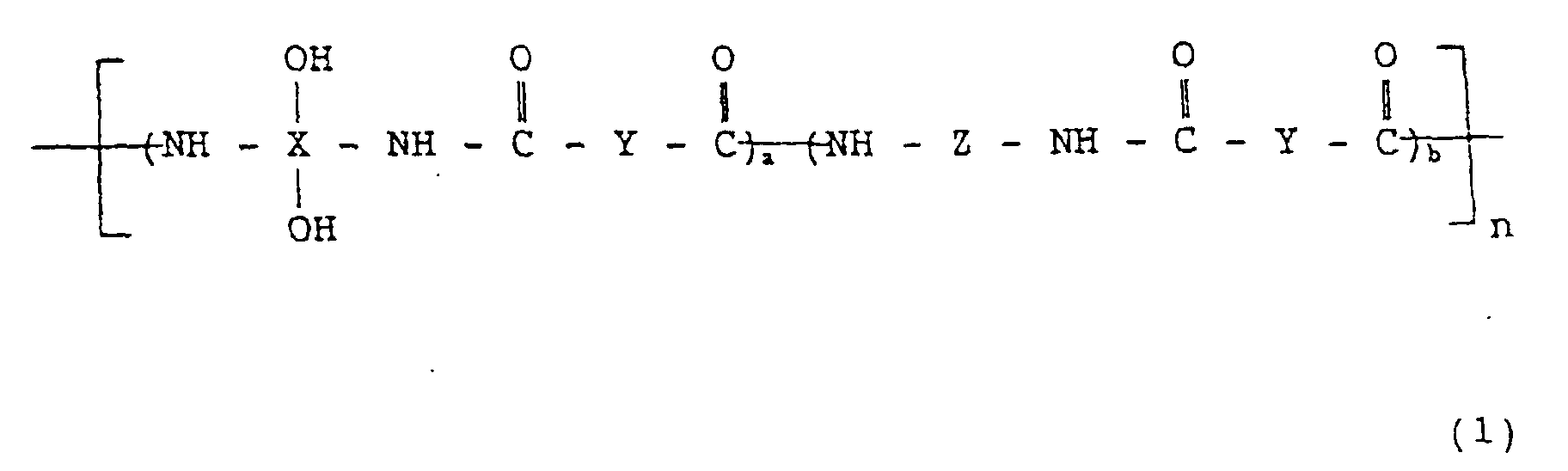
- the polyamide represented by the general formula (1) consists of a bisaminophenol having the X structure, a dicarboxylic acid having the Y structure and optionally a diamine having the Z structure, and this polyamide undergoes ring-closure upon heating at about 300-400°C, to be converted into a polybenzoxazole represented by the above-mentioned general formula (15) which is a heat resistant resin.
- X includes, for example, wherein A represents -CH 2 -, -O-, -S-, -SO 2 -, -CO-, -NHCO, -C(CH 3 ) 2 - or -C(CF 3 ) 2 -.
- those represented by the general formula (12) are preferable because a high sensitivity is imparted by them:
- Y includes, for example, the following groups: wherein A represents -CH 2 -, -O-, -S-, -SO 2 -, -CO-, -NHCO-or -C(CF 3 ) 2 -.
- groups represented by the general formula (13) are preferable because a high sensitivity is imparted by them:
- Z includes, for example,
- Z is used particularly when an adhesion to a substrate such as a silicon wafer is required, and the Z structure can be used in a proportion of at most 40.0 mole %. When the proportion exceeds 40.0 mole %, the solubility of the resin is extremely lowered, scum is produced and the pattern processing becomes impossible.
- each of X, Y and Z may be used alone or in combination of two or more.
- the photosensitive diazoquinone compound used in this invention is a compound having a 1,2-benzoquinone diazide structure or a 1,2-naphthoquinone diazide structure, and is a compound known by USP 2,772,972; 2,797,213 and 3,669,658.
- Said compound includes, for example, compounds represented by the following formulas: wherein Q represents a hydrogen atom; or and in each of the above compounds, at least one Q group is
- the following compounds are preferable in view of high yield of residual film thickness:
- the amount of the photosensitive diazoquinone compound (B) incorporated into the polyamide (A) is 1 to 100 parts by weight per 100 parts by weight of the polyamide (A).
- the amount is less than 1 part by weight, the patterning property of the resin is unsatisfactory, while when the amount exceeds 100 parts by weight, the tensile elongation of the film is remarkably lowered.
- a semiconductor device in which a film having a small tensile elongation is coated on the surface of a semiconductor element is not desirable because the reliability is lowered by a stress such as thermal stress.
- the positive type photosensitive resin composition of this invention can have, if necessary, added thereto a dihydropyridine derivative for enhancing the photosensitive characteristics.
- the dihydropyridine derivative includes, for example, 2,6-dimethyl-3,5-diacetyl-4-(2'-nitrophenyl)-1,4-dihydropyridine, 4-(2'-nitrophenyl)-2,6-dimethyl-3,5-dicarboethoxy-1,4-dihydro-pyridine and 4-(2',4'-dinitrophenyl)-2,6-dimethyl-3,5-dicarbomethoxy-1,4-dihydropyridine.
- the positive type photosensitive resin composition of this invention it is important that at least one member selected from the group consisting of phenol compounds represented by the general formulas (2) and (3) is contained in addition to the above components (A) and (B).
- the dissolution rate in the exposed portion is increased, and the sensitivity is enhanced. Furthermore, the film loss in the unexposed portion as seen when the sensitivity is increased by reducing the molecular weight is very small.
- the phenol compound represented by the general formula (2) or (3) there can be obtained a positive type photosensitive resin composition having such new characteristics that the adhesion of the composition to an encapsulating resin is enhanced, and when this composition is coated on the surface of a semiconductor element, it has been confirmed that the reliability of the semiconductor device is enhanced.
- the compounds represented by the general formula (2) include the following compounds: (m and n are 1 or 2)
- sensitivity and yield of residual film thickness are compounds represented by the structural formulas (6) and (7): and they are preferably contained alone or in combination in the phenol compound (C) in a proportion of at least 50% by weight of the total weight of the phenol compounds.
- the phenol compound represented by the general formula (2) is low in solubility at low temperatures, so that when, for example, a composition containing the phenol compound represented by the general formula (2) is stored at a very low temperature, the deposition of the phenol compound of the general formula (2) is seen in some cases. In such a case, a part of the phenol compound of the general formula (2) can be replaced by a phenol compound of the general formula (3) to enhance the storability at low temperatures.
- the phenol compound represented by the general formula (3) includes the following compounds:
- the amount of the phenol compound (C) added is 1 to 50 parts by weight per 100 parts by weight of the polyamide (A). When the amount is less than 1 part by weight, no effect of increasing the sensitivity is obtained, and when the amount exceeds 50 parts by weight, the reduction of the yield of residual film thickness becomes large or deposition is caused during the storage under refrigeration and hence said amount is poor in practicality.
- the organosilicon compounds (D) represented by the general formulas (8), (9) and (10) in this invention are used for increasing the adhesion between the photosensitive resin and an encapsulating resin. These compounds may be used alone or in admixture of two or more kinds, and the amount of the compound (D) added is 0.1 to 20 parts by weight per 100 parts by weight of the polyamide (A). When the amount is less than 0.1 part by weight, no effect of enhancing the adhesion is obtained, and when the amount exceeds 20 parts by weight, the mechanical strength of the film of polybenzoxazole formed on a semiconductor element is lowered and the stress-relaxing effect becomes small, so that the above amounts are not desirable.
- the organosilicon compound represented by the general formula (8) is disclosed in USP 3,755,354 and 4,460,739 and hence is a known compound.
- the present inventors have found that when this organosilicon compound is added to such a photosensitive polybenzoxazole precursor as shown in JP-B-1-46,862, there can be obtained such a high adhesion to a silicon wafer as not obtained with the conventional silane coupling agent.
- the organosilicon compound represented by the general formula (9) is described in JP-A-1-215,869 and is a known material used as one of the starting materials for a curable composition for forming a protective film for a transparent plate or a color filter.
- the organosilicon compounds represented by the general formulas (8) and (9) can be easily obtained by subjecting an acid anhydride or dianhydride and a silane coupling agent having an amino group to reaction at 20-100°C for 30 minutes to 10 hours in an organic solvent.
- the acid anhydride used includes, for example, maleic anhydride, succinic anhydride, methyltetrahydrophthalic anhydride, methylhexahydrophthalic anhydride, methyl-himic anhydride, hexahydrophthalic anhydride, tetrahydrophthalic anhydride and phthalic anhydride.
- acid dianhydride examples include, for example, pyrromellitic dianhydride, benzene-1,2,3,4-tetracarboxylic dianhydride, 3,3',4,4'-benzophenonetetracarboxylic dianhydride, 2,2',3,3'-benzophenonetetracarboxylic dianhydride, 2,2,3',4'-benzophenonetetracarboxylic dianhydride, naphthalene-2,3,6,7-tetracarboxylic dianhydride, naphthalene-1,2,5,6-tetracarboxylic dianhydride, naphthalene-1,2,4,5-tetracarboxylic dianhydride, naphthalene-1,4,5,8-tetracarboxylic dianhydride, naphthalene-1,2,6,7-tetracarboxylic dianhydride, 4,8-dimethyl-1,2,3,5,6,7-hexahydron
- silane coupling agent having an amino group examples include ⁇ -aminopropyltrimethoxysilane, ⁇ -aminopropyltriethoxysilane, ⁇ -aminopropylmethyldiethoxysilane, ⁇ -aminopropylmethyldimethoxysilane, ⁇ -aminopropylethyldimethoxysilane, ⁇ -aminopropylethyldiethoxysilane, ⁇ -aminopropyldimethylmethoxysilane, ⁇ -aminopropyldimethylethoxysilane, ⁇ -aminopropyldiethylmethoxysilane, ⁇ -aminopropyldiethylethoxysilane, N-( ⁇ -aminoethyl)- ⁇ -aminopropyltrimethoxysilane, N-( ⁇ -aminoethyl)- ⁇ -aminopropyltriethoxysi
- the organosilicon compound represented by the general formula (10) is easily obtained by subjecting a silane-coupling agent having an epoxy group and a tetracarboxylic dianhydride to reaction at a temperature of 20 to 100°C for a period of 30 minutes to 10 hours.
- a silane-coupling agent having an epoxy group and a tetracarboxylic dianhydride to reaction at a temperature of 20 to 100°C for a period of 30 minutes to 10 hours.
- Examples of the acid dianhydride are the same as mentioned for the organosilicon compound represented by the general formula (9).
- silane-coupling agent examples include ⁇ -glycidoxypropyltrimethoxysilane, ⁇ -glycidoxypropyltriethoxysilane, ⁇ -glycidoxypropylmethyldimethoxysilane, ⁇ -glycidoxypropylmethyldiethoxysilane, ⁇ -glycidoxypropylethyldimethoxysilane, ⁇ -glycidoxypropylethyldiethoxysilane, ⁇ -glycidoxypropyldimethylmethoxysilane, ⁇ -glycidoxypropyldimethylethoxysilane, ⁇ -glycidoxypropyldiethylmethoxysilane and ⁇ -glycidoxypropyldiethylethoxysilane.
- an additive such as a leveling agent or a silane-coupling agent.
- the above-mentioned components are dissolved in a solvent to form a varnish and this varnish is used.
- a solvent there may be used alone or in admixture N-methyl-2-pyrrolidone, ⁇ -butyrolactone, N,N-dimethylacetamide, dimethylsulfoxide, diethylene glycol dimethyl ether, diethylene glycol diethyl ether, diethylene glycol dibutyl ether, propylene glycol monomethyl ether, dipropylene glycol monomethyl ether, propylene glycol monomethyl ether acetate, methyl lactate, ethyl lactate, butyl lactate, methyl-1,3-butylene glycol acetate, 1,3-butylene glycol 3-monomethyl ether, methyl pyruvate, ethyl pyruvate and methyl 3-methoxypropionate .
- the composition is coated on a suitable support, for example, a silicon wafer, a ceramic plate or an aluminum plate.
- the coating method includes a spin coating using a spinner, a spray coating using a spray coater, an immersion, a printing and a roll coating.
- the resulting support is prebaked at a temperature of 60 to 120°C to dry the coating film and thereafter irradiated with an actinic radiation or with an electronic beam in the form of the desired pattern.
- the actinic radiation there can be used X ray, ultraviolet ray and visible ray; and, it is preferable to use an actinic radiation having a wavelength of 200 to 500 nm.
- an aqueous solution of an alkali for example, an inorganic alkali such as sodium hydroxide, potassium hydroxide, sodium carbonate, sodium silicate, sodium metasilicate or ammonia water ; a primary amine such as ethylamine or n-propylamine ; a secondary amine such as diethylamine or di-n-propylamine ; a tertiary amine such as triethylamine or (methyldiethylamine ; an alcoholamine such as dimethylethanolamine or triethanol-amine; a quaternary ammonium salt such as tetramethylammonium hydroxide or tetraethylammonium hydroxide , or there can also be used an aqueous solution formed by adding to the above alkali solution suitable amounts of a water-soluble organic solvent, for example
- the development method there can be used spray, paddle, immersion or ultrasonic wave. Subsequently, the relief pattern formed by the development is rinsed. As the rinse, distilled water is used. Subsequently, the rinsed pattern is heat-treated to form an oxazole ring, thereby obtaining the final pattern rich in heat resistance.
- the positive type photosensitive resin composition of this invention is useful for not only semiconductor applications but also interlaminar insulation of a multilayer circuit and also useful as a cover coat of a flexible copper-clad laminate, a solder resist film or a liquid crystal alignment layer.
- N-methyl-2-pyrrolidone 100 parts by weight of the polyamide (A1) obtained above, 25 parts by weight of a diazoquinone represented by the general formula (Q1): wherein Q represents a hydrogen atom or and and 70% of a total of the Q groups is and 15 parts by weight of a phenol compound represented by the structural formula (P-1): and thereafter, filtered through a 0.2- ⁇ m Teflon TM filter to obtain a photosensitive resin composition.
- Q1 diazoquinone represented by the general formula (Q1): wherein Q represents a hydrogen atom or and and 70% of a total of the Q groups is and 15 parts by weight of a phenol compound represented by the structural formula (P-1):
- This positive type photosensitive resin composition was coated on a silicon wafer by use of a spin coater and thereafter dried at 70°C for one hour in an oven to obtain a coating film having a thickness of about 3 ⁇ m.
- This coating film was exposed to light through a reticle by a g-line stepper exposing machine NSR-1505G3A (a trade name of NIKON CORP.) while changing the exposing portion of the coating film and increasing the exposure dose from 50 mJ/cm 2 to 540 mJ/cm 2 at a rate of 10 mJ/cm 2 .
- the exposed coating film was immersed in a 0.79% aqueous solution of tetramethylammonium hydroxide for 30 seconds to dissolve and remove the exposed portion and then rinsed with pure water for 30 seconds.
- a pattern was formed in the portion irradiated at an exposure dose of 200 mJ/cm 2 or more (namely, the sensitivity was 200 mJ/cm 2 ).
- the yield of residual film thickness at this time [(film thickness after development/film thickness before development) x 100] was 91.3% which was a very high value.
- the same positive type photosensitive resin composition was similarly coated on a silicon wafer, prebaked and thereafter heated in an oven at 150°C for 30 minutes, at 250°C for 30 minutes and at 350°C for 30 minutes in this order to cure the resin.
- a semiconductor-encapsulating epoxy resin composition (EME-6300H, a trade name of Sumitomo Bakelite Co., Ltd.) was molded in a size of 2 x 2 x 2 mm (width x length x height).
- EME-6300H a trade name of Sumitomo Bakelite Co., Ltd.
- the encapsulating epoxy resin composition molded on the cured film of a polybenzoxazole resin was peeled away to measure the shear strength. The result thereof was 3.2 kg/mm 2 .
- Example 1 The same procedure as in Example 1 was repeated, except that the phenol compound (P-1) was replaced by a mixture of phenol compounds represented by the structural formulas (P-3): to obtain the results shown in Table 1.
- Example 1 The same procedure as in Example 1 was repeated, except that the amount of the phenol compound (P-1) added was changed to 5 parts by weight, to obtain the results shown in Table 1.
- X is a t
- X is a tetravalent group represented by the above-mentioned formula (X-1)
- Y
- Example 1 The same procedure as in Example 1 was repeated, except that the phenol compound was not added, to obtain the results shown in Table 1.
- Example 5 The same procedure as in Example 5 was repeated, except that the phenol compound was not added, to obtain the results shown in Table 1.
- Example 1 The same procedure as in Example 1 was repeated, except that the amount of the phenol compound added was decreased to 0.5 part by weight, to obtain the results shown in Table 1.
- Example 1 The same procedure as in Example 1 was repeated, except that the amount of the phenol compound added was increased to 60 parts by weight, to obtain the results shown in Table 1.
- Example 1 The same procedure as in Example 1 was repeated, except that the phenol compound was replaced by a phenol compound represented by the structural formula (P-4): to obtain the results shown in Table 1.
- Example 1 The same procedure as in Example 1 was repeated, except that the phenol compound was replaced by a phenol compound represented by the structural formula (P-5): to obtain the results shown in Table 1.
- Example 1 The same procedure as in Example 1 was repeated, except that the phenol compound was replaced by a phenol compound represented by the structural formula (P-6): to obtain the results shown in Table 1.
- This photosensitive resin composition in the form of a varnish was coated on a silicon wafer using a spin coater, and thereafter, dried at 70°C for one hour in an oven to obtain a coating film having a thickness of about 6 ⁇ m.
- This coating film was irradiated with an ultraviolet ray from a high pressure mercury vapor lamp through a mask manufactured by TOPPAN PRINTING CO., LTD. (test chart No. 1, on which line and space of 50-0.88 ⁇ m in width were drawn), then immersed in a 0.79% aqueous solution of tetramethylammonium hydroxide for 60 seconds to dissolve and remove the exposed portion and thereafter washed with pure water for 30 seconds (rinse) to remove the developer.
- the same photosensitive resin composition varnish was coated on a silicon wafer in the same manner, prebaked and then heated in an oven at 150°C for 30 minutes, at 250°C for 30 minutes and at 350°C for 30 minutes in this order to cure the resin.
- the coating film obtained was cross-cut in 1-mm width to form 100 squares, and a Cellophane TM tape was applied to the coating film and then peeled off in order to remove the coating film squares from the silicon wafer.
- the number of the coating film squares removed (referred to hereinafter as the number of peeled squares after curing) was 0, from which it was confirmed that also the adhesion of the cured film to the wafer was excellent.
- the silicon wafer was subjected to pressure cooker treatment (PCT) at 125°C at 2,33 10 5 Pa (2.3 atm) for 100 hours and thereafter, a Cellophane TM tape was applied thereto and peeled off in the same manner as above to evaluate the adhesion.
- PCT pressure cooker treatment
- the number of the coating film squares removed (referred to hereinafter as the number of peeled squares after high temperature-high humidity treatment) was 0, from which it was confirmed that the adhesion after high temperature-high humidity treatment was excellent.
- Example 9 The same procedure as in Example 9 was repeated, except that the organosilicon compound was replaced by a compound represented by the structural formula (S-3): to obtain the results shown in Table 2.
- Example 9 The same procedure as in Example 9 was repeated, except that the polyamide was replaced by the polyamide (A2) synthesized in Example 5, to obtain the results shown in Table 2.
- Example 9 The same procedure as in Example 9 was repeated, except that the polyamide was replaced by the polyamide (A3) synthesized in Example 6, to obtain the results shown in Table 2.
- Example 9 The same procedure as in Example 9 was repeated, except that the polyamide was replaced by the polyamide (A4) synthesized in Example 7 and the diazoquinone was replaced by a diazoquinone represented by the above-mentioned general formula (Q2), to obtain the results shown in Table 2.
- Example 9 The same procedure as in Example 9 was repeatexcept that the polyamide was replaced by the polyamide (A5) synthesized in Example 8, to obtain the results shown in Table 2.
- Example 9 The same procedure as in Example 9 was repeated, except that the amount of the organosilicon compound added was reduced to 0.05 part by weight, to obtain the results shown in Table 2.
- Example 9 The same procedure as in Example 9 was repeated, except that the amount of the organosilicon compound added was increased to 50 parts by weight, to obtain the results shown in Table 2.
- Example 9 The same procedure as in Example 9 was repeated, except that the organosilicon compound was replaced by an organosilicon compound represented by the structural formula (S-4): to obtain the results shown in Table 2.
- Example 9 The same procedure as in Example 9 was repeated, except that the organosilicon compound was replaced by an organosilicon compound represented by the structural formula (S-5): to obtain the results shown in Table 2.
- Example 9 The same procedure as in Example 9 was repeated, except that the organosilicon compound was replaced by an organosilicon compound represented by the structural formula (S-6): (C 2 H 5 O) 3 SiC 3 H 6 -NH 2 to obtain the results shown in Table 2.
- organosilicon compound represented by the structural formula (S-6): (C 2 H 5 O) 3 SiC 3 H 6 -NH 2 to obtain the results shown in Table 2.
- N-methyl-2-pyrrolidone 100 parts by weight of the polyamide (A1) synthesized in Example 1, 25 parts by weight of a diazoquinone represented by the above-mentioned structural formula (Q1) and 6 parts by weight of an organosilicon compound represented by the structural formula (S-7): and then filtered through a 0.2- ⁇ m Teflon TM filter to obtain a photosensitive resin composition.
- This photosensitive resin composition in the form of a varnish was coated on a silicon wafer using a spin coater, and thereafter, dried at 70°C for one hour in an oven to obtain a coating film having a thickness of about 6 ⁇ m.
- This coating film was irradiated with an ultraviolet ray from a high pressure mercury vapor lamp through a mask manufactured by TOPPAN PRINTING CO., LTD. (test chart No. 1, on which line and space of 50-0.88 ⁇ m in width were drawn), then immersed in a 0.79% aqueous solution of tetramethylammonium hydroxide for 60 seconds to dissolve and remove the exposed portion and thereafter washed with pure water for 30 seconds (rinse) to remove the developer.
- the same photosensitive resin composition varnish was coated on a silicon wafer in the same manner, prebaked and then heated in an oven at 150°C for 30 minutes, at 250°C for 30 minutes and at 350°C for 30 minutes in this order to cure the resin.
- the coating film obtained was cross-cut in 1-mm width to form 100 squares, and a Cellophane TM tape was applied to the coating film and then peeled off in order to remove the coating film squares from the silicon wafer.
- the number of the coating film squares removed (referred to hereinafter as the number of peeled squares after curing) was 0, from which it was confirmed that also the adhesion of the cured film to the wafer was excellent.
- the silicon wafer was subjected to pressure cooker treatment (PCT) at 125°C at 2,33 10 5 Pa (2.3 atm) for 100 hours and thereafter, a Cellophane TM tape was applied thereto and peeled off in the same manner as above to evaluate the adhesion.
- the number of the coating film squares removed (referred to hereinafter as the number of peeled squares after high temperature-high humidity treatment) was 0, from which it was confirmed that also the adhesion after high temperature-high humidity treatment was excellent.
- the above photosensitive resin composition varnish was stored in a refrigerator at -20°C for 30 days, deposits and the like were not seen, from which it was confirmed that the photosensitive resin composition varnish had a good storability.
- Example 17 The same procedure as in Example 17 was repeated, except that the organosilicon compound was replaced by a organosilicon compound represented by the structural formula (S-8): to obtain the results shown in Table 3.
- Example 17 The same procedure as in Example 17 was repeated, except that the organosilicon compound was replaced by a organosilicon compound represented by the structural formula (S-9): to obtain the results shown in Table 3.
- Example 17 The same procedure as in Example 17 was repeated, except that the organosilicon compound was replaced by a organosilicon compound represented by the structural formula (S-10): to obtain the results shown in Table 3.
- Example 17 The same procedure as in Example 17 was repeated, except that the polyamide was replaced by the polyamide (A2) synthesized in Example 5, to obtain the results shown in Table 3.
- Example 17 The same procedure as in Example 17 was repeated, except that the polyamide was replaced by the polyamide (A3) synthesized in Example 6, to obtain the results shown in Table 3.
- Example 17 The same procedure as in Example 17 was repeated, except that the polyamide was replaced by the polyamide (A4) synthesized in Example 7 and the diazoquinone was replaced by a diazoquinone represented by the above-mentioned structural formula (Q2), to obtain the results shown in Table 3.
- Example 17 The same procedure as in Example 17 was repeated, except that the polyamide was replaced by the polyamide (A5) synthesized in Example 8, to obtain the results shown in Table 3.
- Example 17 The same procedure as in Example 17 was repeated, except that the amount of the organosilicon compound added was reduced to 0.05 part by weight, to obtain the results shown in Table 3.
- Example 17 The same procedure as in Example 17 was repeated, except that the amount of the organosilicon compound was increased to 50 parts by weight, to obtain the results shown in Table 3.
- Example 17 The same procedure as in Example 17 was repeated, except that the organosilicon compound was replaced by an organosilicon compound represented by the structural formula (S-11): to obtain the results shown in Table 3.
- Example 17 The same procedure as in Example 17 was repeated, except that the organosilicon compound was replaced by an organosilicon compound represented by the structural formula (S-12): to obtain the results shown in Table 3.
- Example 17 The same procedure as in Example 17 was repeated, except that the organosilicon compound was replaced by an organosilicon compound represented by the structural formula (S-13): (C 2 H 5 O) 3 SiC 3 H 6 -NH 2 to obtain the results shown in Table 3.
- organosilicon compound represented by the structural formula (S-13): (C 2 H 5 O) 3 SiC 3 H 6 -NH 2 to obtain the results shown in Table 3.
- Example 2 In the same procedure as in Example 1, the synthesis of a polyamide, the preparation of a positive type photosensitive resin composition and the evaluation of characteristics (sensitivity, yield of residual film thickness and shear strength) were conducted.
- the positive type photosensitive resin composition obtained above was coated on an element wafer provided with an aluminum circuit on its surface so that the final film thickness became 5 ⁇ m, then subjected to pattern processing and finally baked.
- the product was divided into every chip size and mounted on a lead frame for 16-pin DIP (dual inline package) with an electroconductive paste and then encapsulated with a semiconductor-encapsulating epoxy resin (EME-6300H, a trade name of Sumitomo Bakelite Co., Ltd.) to obtain a 16-pin DIP.
- a semiconductor-encapsulating epoxy resin EME-6300H, a trade name of Sumitomo Bakelite Co., Ltd.
- the package was treated under the conditions of 85°C/85% humidity for 168 hours, and then immersed in a solder bath at 260°C for 10 seconds and thereafter subjected to pressure cooker treatment at a high temperature at a high humidity (125°C, 2,33 10 5 Pa (2.3 atm), 100% RH), after which the failure of opening of the aluminum circuit was checked.
- the results obtained are shown in Table 4.
- Example 26 The same procedure as in Example 26 was repeated, except that the positive type photosensitive resin composition was replaced by those shown in Table 4 to obtain the results shown in Table 4.
- Example 26 The same procedure as in Example 26 was repeated, except that the polybenzoxazole resin was not coated on the element surface in the evaluation of reliability of semiconductor device, to obtain the results shown in Table 4.
- Example 26 In the evaluation of resin characteristics in Example 26, the pattern processing was conducted in a film thickness of 30 ⁇ m. As a result, even in an exposure dose of 1,000 mJ/cm 2 , the resin remained in the exposed portion after the development and patterning was impossible.
- Example 26 The same procedure as in Example 26 was repeated, except that the positive type photosensitive resin composition was replaced by the positive type photosensitive resin composition obtained in Comparative Example 1, to obtain the results shown in Table 4.
- Example 30 The same procedure as in Example 30 was repeated, except that the phenol compound was not added, to obtain the results shown in Table 4.
- Example 31 The same procedure as in Example 31 was repeated, except that the phenol compound was not added, to obtain the results shown in Table 4.
- Example 26 The same procedure as in Example 26 was repeated, except that the amount of the phenol compound added was reduced to 0.5 part by weight, to obtain the results shown in Table 4.
- Example 26 The same procedure as in Example 26 was repeated, except that the amount of the phenol compound added was increased to 60 parts by weight, to obtain the results shown in Table 4.
- Example 26 The same procedure as in Example 26 was repeated, except that the phenol compound was replaced by a phenol compound represented by the above-mentioned structural formula (P-4), to obtain the results shown in Table 4.
- Example 26 The same procedure as in Example 26 was repeated, except that the phenol compound was replaced by a phenol compound represented by the above-mentioned structural formula (P-5), to obtain the results shown in Table 4.
- Example 26 The same procedure as in Example 26 was repeated, except that the phenol compound was replaced by a phenol compound represented by the above-mentioned structural formula (P-6) to obtain the results shown in Table 4.
- N-methylpyrrolidone 100 parts by weight of the polyamide (A1) synthesized in Example 1, 25 parts by weight of a diazoquinone represented by the above-mentioned structural formula (Q1), 15 parts by weight of a phenol compound represented by the above-mentioned structural formula (P-1), 2.0 parts by weight of an organosilicon compound represented by the above-mentioned structural formula (S-1) obtained by reacting ⁇ -aminopropyltriethoxysilane with maleic anhydride and 1.0 part by weight of an organosilicon compound represented by the above-mentioned structural formula (S-8) obtained by reacting ⁇ -aminopropyltriethoxysilane with 3,3',4,4'-benzophenonetetracarboxylic dianhydride, and thereafter, filtered through a 0.2- ⁇ m TeflonTM filter to obtain a photosensitive resin composition.
- This positive type photosensitive resin composition was coated on a silicon wafer by use of a spin coater and thereafter dried at 70°C for one hour in an oven to obtain a coating film having a thickness of about 5 ⁇ m.
- This coating film was exposed to light through a reticle by a g-line stepper exposing machine NSR-1505G3A (a trade name of NIKON CORP.) while changing the exposing portion of the coating film and increasing the exposure dose from 50 mJ/cm 2 to 540 mJ/cm 2 at a rate of 10 mJ/cm 2 .
- the exposed coating film was immersed in a 0.79% aqueous solution of tetramethylammonium hydroxide for 30 seconds to dissolve and remove the exposed portion and then rinsed with pure water for 30 seconds.
- a pattern was formed in the portion irradiated at an exposure dose of 200 mJ/cm 2 or more (namely, the sensitivity was 200 mJ/cm 2 ).
- the yield of residual film thickness at this time [(film thickness after development/film thickness before development) x 100] was 91.3% which was a very high value.
- the same positive type photosensitive resin composition was similarly coated on a silicon wafer, prebaked and thereafter heated in an oven at 150°C for 30 minutes, at 250°C for 30 minutes and at 350°C for 30 minutes in this order to cure the resin.
- a semiconductor-encapsulating epoxy resin composition (EME-6300H, a trade name of Sumitomo Bakelite Co., Ltd.) was molded in a size of 2 x 2 x 2 mm (width x length x height).
- EME-6300H a trade name of Sumitomo Bakelite Co., Ltd.
- the encapsulating epoxy resin composition molded on the cured film of a polybenzoxazole resin was peeled to measure the shear strength. The result thereof was 4.5 kg/mm 2 .
- the above positive type photosensitive resin composition was coated on an element wafer provided with an aluminum circuit on its surface so that the final film thickness became 5 ⁇ m, then subjected to pattern processing and finally baked.
- the product was divided into every chip size and mounted on a lead frame for 16-pin DIP (dual inline package) with an electroconductive paste and then encapsulated with a semiconductor-encapsulating epoxy resin (EME-6300H, a trade name of Sumitomo Bakelite Co., Ltd.) to obtain a 16-pin DIP.
- a semiconductor-encapsulating epoxy resin EME-6300H, a trade name of Sumitomo Bakelite Co., Ltd.
- the package was treated under the conditions of 85°C/85% humidity for 168 hours, and then immersed in a solder bath at 260°C for 10 seconds and thereafter subjected to pressure cooker treatment at a high temperature at a high humidity (125°C, 2,33 10 5 Pa (2.3 atm), 100% RH), after which the failure of opening of the aluminum circuit was checked.
- the results obtained are shown in Table 5.
- Example 34 The same procedure as in Example 34 was repeated, except that the phenol compound was replaced by a phenol compound represented by the above-mentioned structural formula (P-2), to obtain the results shown in Table 5.
- Example 34 The same procedure as in Example 34 was repeated, except that the phenol compound was replaced by a phenol compound represented by the above-mentioned structural formula (P-3), to obtain the results shown in Table 5.
- Example 34 The same procedure as in Example 34 was repeated, except that the amount of the phenol compound (P-1) added was changed to 5 parts by weight, to obtain the results shown in Table 5.
- Example 34 The same procedure as in Example 34 was repeated, except that the polyamide (A1) was replaced by the polyamide (A2) synthesized in Example 5, to obtain the results shown in Table 5.
- Example 34 The same procedure as in Example 34 was repeated, except that the polyamide (A1) was replaced by the polyamide (A3) synthesized in Example 6 and the organosilicon compound was replaced by an organosilicon compound represented by the above-mentioned structural formula (S-7) obtained by reacting ⁇ -aminopropyltriethoxysilane with 3,3',4,4'-oxydiphthalic dianhydride, to obtain the results shown in Table 5.
- Example 34 The same procedure as in Example 34 was repeated, except that the polyamide (A1) was replaced by the polyamide (A4) synthesized in Example 7, the diazoquinone was replaced by a diazoquinone represented by the above-mentioned structural formula (Q2) and the organosilicon compound was replaced by 1.0 part by weight of an organosilicon compound represented by the structural formula (S-1) obtained by reacting ⁇ -aminopropyltriethoxysilane with maleic anhydride, 0.5 part by weight of an organosilicon compound represented by the above-mentioned structural formula (S-7) obtained by reacting ⁇ -aminopropyltriethoxysilane with 3,3',4,4'-oxydiphthalic dianhydride and 0.5 part by weight of an organosilicon compound represented by the structural formula (S-14): obtained by reacting ⁇ -glycidoxypropyltrimethoxysilane with 3,3',4,4'-benzophenonetetracarboxylic dian
- Example 34 The same procedure as in Example 34 was repeated, except that the polyamide (A1) was replaced by the polyamide (A5) synthesized in Example 8, to obtain the results shown in Table 5.
- Example 34 The same procedure as in Example 34 was repeated, except that the phenol compound was not added, to obtain the results shown in Table 5.
- Example 38 The same procedure as in Example 38 was repeated, except that the phenol compound was not added, to obtain the results shown in Table 5.
- Example 39 The same procedure as in Example 39 was repeated, except that the phenol compound was not added, to obtain the results shown in Table 5.
- Example 34 In the evaluation of the resin characteristics in Example 34, a coating film having a thickness of 30 ⁇ m was patterned. However, even in an exposure dose of 1,000 mJ/cm 2 , the resin remained in the exposed portion after the development and the patterning was impossible.
- Example 34 The same procedure as in Example 34 was repeated, except that the amount of the phenol compound added was increased to 60 parts by weight, to obtain the results shown in Table 5.
- Example 34 The same procedure as in Example 34 was repeated, except that the amount of the organosilicon compound represented by the above-mentioned structural formula (S-1) obtained by reacting ⁇ -aminopropyltriethoxysilane with maleic anhydride was increased to 15.0 parts by weight, and the amount of the organosilicon compound represented by the above-mentioned structural formula (S-8) obtained by reacting ⁇ -aminopropyltriethoxysilane with 3,3',4,4'-benzophenonetetracarboxylic dianhydride was increased to 10.0 parts by weight, to obtain the results shown in Table 5.
- S-1 organosilicon compound represented by the above-mentioned structural formula (S-1) obtained by reacting ⁇ -aminopropyltriethoxysilane with maleic anhydride was increased to 15.0 parts by weight
- S-8 the amount of the organosilicon compound represented by the above-mentioned structural formula (S-8) obtained by reacting ⁇ -
- Example 34 The same procedure as in Example 34 was repeated, except that the phenol compound was replaced by a phenol compound represented by the above-mentioned structural formula (P-4), to obtain the results shown in Table 5.
- Example 34 The same procedure as in Example 34 was repeated, except that the phenol compound was replaced by a phenol compound represented by the above-mentioned structural formula (P-5) to obtain the results shown in Table 5.
- Examples 34-44 and Comparative Examples 35-40 are summarized in the following Table 5.
- a positive type photosensitive resin composition which is excellent in adhesion to an encapsulating resin and a substrate, which has a high sensitivity and which can give a pattern with a high yield of residual film thickness
- a semiconductor device having a high reliability in which a pattern of a polybenzoxazole resin has been formed with a high yield of residual film thickness on a semiconductor element using the positive type photosensitive resin composition excellent in adhesion to an encapsulating resin.
Landscapes
- Physics & Mathematics (AREA)
- General Physics & Mathematics (AREA)
- Spectroscopy & Molecular Physics (AREA)
- Materials For Photolithography (AREA)
- Macromolecular Compounds Obtained By Forming Nitrogen-Containing Linkages In General (AREA)
Claims (28)
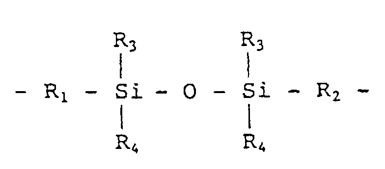
- Composition de résine photosensible de type positif, qui contient :(A) 100 parties en poids d'un polyamide représenté par la formule générale (1) :dans laquelle X représente un groupe aromatique tétravalent; Y représente un groupe aromatique divalent; Z représente un groupe divalent décrit par la formule :
 dans laquelle R1 et R2 représentent des groupes organiques divalents, et R3 et R4 représentent des groupes organiques monovalents; a et b représentent des fractions molaires; a + b = 100 % molaires; a = 60,0 à 100,0 % molaires; b = 0 à 40,0 % molaires; et n représente un entier de 2 à 500,
 (B) 1 à 100 parties en poids d'un composé diazoquinone photosensible, et(C) 1 à 50 parties en poids d'au moins un élément choisi dans l'ensemble constitué des composés phénoliques représentés par les formules générales (2) et (3) :dans laquelle R5 et R6 représentent des atomes d'hydrogène ou des groupes alkyle; et chaque groupe R7, R8, R9 et R10 représente un atome d'hydrogène, un groupe hydroxyle, ou un groupe alkyle,
 dans laquelle R11 représente un atome d'hydrogène ou un groupe alkyle;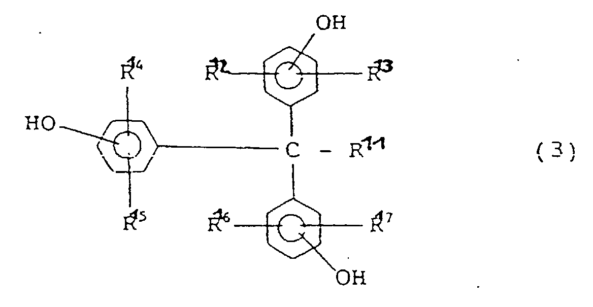
et chacun des groupes R12, R13, R14, R15, R16, et R17 représente un atome d'hydrogène, un atome d'halogène, un groupe hydroxyle, un groupe alkyle, ou un groupe alicyclique. - Composition à base de résine photosensible de type positif selon la revendication 1, dans laquelle le composé phénolique (C) est au moins un élément choisi dans l'ensemble constitué des composés phénoliques représentés par les formules structurelles (4) et (5) :


- Composition à base de résine photosensible de type positif selon la revendication 2, dans laquelle le composé phénolique (C) comprend les composés phénoliques représentés par les formules structurelles (6) et (7), seuls ou en mélange, dans une proportion d'au moins 50 % en poids du poids total des composés phénoliques (C) :


- Composition à base de résine photosensible de type positif, qui comprend :(A) 100 parties en poids d'un polyamide représenté par la formule générale (1) définie dans la revendication 1,(B) 1 à 100 parties en poids d'un composé diazoquinone photosensible, et(D) 0,1 à 20 parties en poids d'au moins un élément choisi dans l'ensemble constitué des composés organosiliciques représentés par les formules générales (8), (9) et (10) :dans laquelle R18 représente un groupe organique divalent; R19 représente un groupe organique divalent; R20 et R21 peuvent être identiques ou différents l'un de l'autre, et représentent chacun un groupe organique monovalent; et représente un entier égal à 0, 1 ou 2,
 dans laquelle R22 représente un groupe aromatique tétravalent; R23 représente un groupe organique divalent; R24 et R25 peuvent être identiques ou différents l'un de l'autre, et représentent chacun un groupe organique monovalent; et ℓ représente un entier égal à 0, 1 ou 2, et
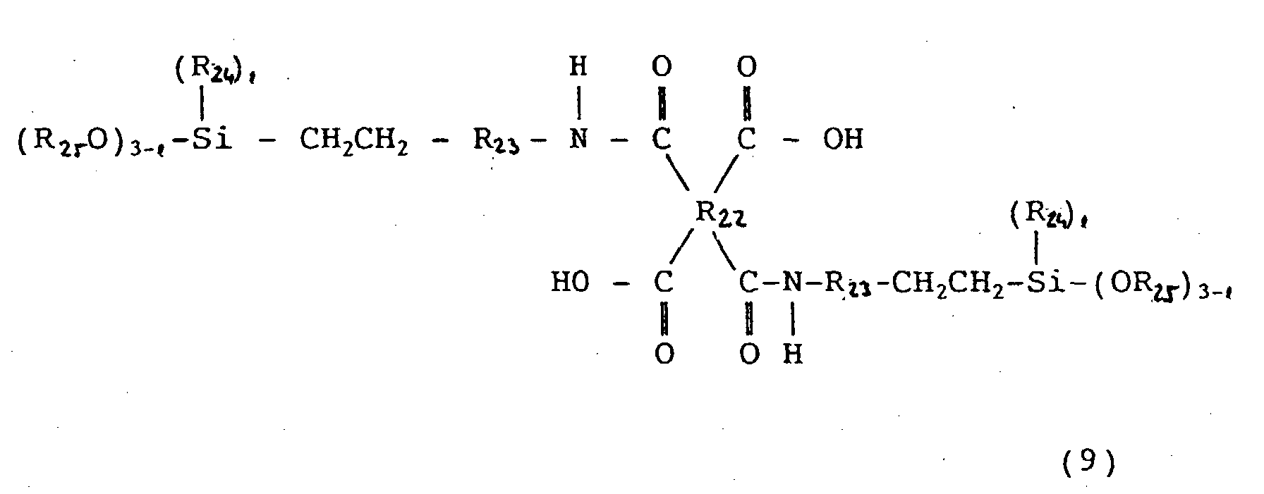 dans laquelle R26 représente un groupe aromatique tétravalent; R27 représente un groupe organique divalent; R28 et R29 peuvent être identiques ou différents l'un de l'autre, et représentent chacun un groupe organique monovalent; et représente un entier égal à 0, 1 ou 2.
- Composition à base de résine photosensible de type positif selon la revendication 4, dans laquelle R18, dans la formule générale (8), est -CH=CH-.
- Composition à base de résine photosensible de type positif selon la revendication 4, dans laquelle R22, dans la formule générale (9), est choisi dans l'ensemble constitué des groupes tétravalents représentés par les formules (11) suivantes :

- Composition à base de résine photosensible de type positif selon l'une quelconque des revendications 1 à 6, dans laquelle X, dans la formule générale (1), est choisi dans l'ensemble constitué des groupes tétravalents représentés par les formules (12) :

- Composition à base de résine photosensible de type positif selon l'une quelconque des revendications 1 à 7, dans laquelle Y, dans la formule générale (1), est choisi dans l'ensemble constitué des groupes divalents représentés par les formules (13) :

- Composition à base de résine photosensible de type positif selon l'une quelconque des revendications 1 à 8, dans laquelle le composé diazoquinone photosensible (B) est choisi dans l'ensemble constitué des composés représentés par les formules générales (14) :
 dans lesquelles Q représente un atome d'hydrogène ou un groupe décrit par la formule :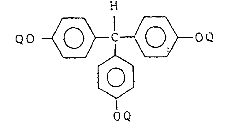

- Composition à base de résine photosensible de type positif, qui comprend :(A) 100 parties en poids d'un polyamide représenté par la formule générale (1) définie dans la revendication 1,(B) 1 à 100 parties en poids d'un composé diazoquinone photosensible,(C) 1 à 50 parties en poids d'au moins un élément choisi dans l'ensemble constitué des composés phénoliques représentés par les formules générales (2) et (3) définies dans la revendication 1, et(D) 0,1 à 20 parties en poids d'au moins un élément choisi dans l'ensemble constitué des composés organosiliciques représentés par les formules générales (8), (9) et (10), définies dans la revendication 4.
- Composition à base de résine photosensible de type positif selon la revendication 10, dans laquelle le composé phénolique (C) est au moins un élément choisi dans l'ensemble constitué des composés phénoliques représentés par les formules structurelles (4) et (5) définies dans la revendication 2.
- Composition à base de résine photosensible de type positif selon la revendication 10 ou 11, dans laquelle le composé phénolique (C) comprend les composés phénoliques représentés par les formules structurelles (6) et (7) définies dans la revendication 3, seuls ou en mélange, dans une proportion d'au moins 50 % en poids du poids total des composés phénoliques (C).
- Composition à base de résine photosensible de type positif selon la revendication 10, 11, ou 12, dans laquelle X, dans la formule générale (1), est choisi dans l'ensemble constitué des groupes tétravalents représentés par les formules (12) définies dans la revendication 7.
- Composition à base de résine photosensible de type positif selon la revendication 10, 11, 12, ou 13, dans laquelle Y, dans la formule générale (1), est choisi parmi les groupes divalents représentés par les formules (13) définies dans la revendication 8.
- Composition à base de résine photosensible de type positif selon la revendication 10, 11, 12, 13 ou 14, dans laquelle le composé diazoquinone photosensible (B) est choisi parmi les composés représentés par les formules générales (14) définies dans la revendication 9.
- Dispositif semi-conducteur dans lequel une pellicule en résine polybenzoxazole, formée à partir de la composition à base de résine photosensible de la revendication 1, 4, ou 10, et représentée par la formule générales (15) :dans laquelle X représente un groupe aromatique tétravalent; Y représente un groupe aromatique divalent; Z représente un groupe divalent représenté par la formule :
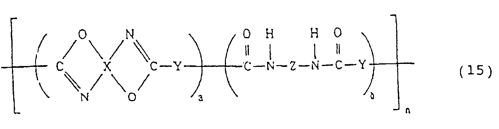 dans laquelle R1 et R2 représentent des groupes organiques divalents, et R3 et R4 représentent des groupes organiques monovalents; a et b représentent des fractions molaires; a + b = 100 % molaires; a = 60,0 à 100,0 % molaires; b = 0 à 40,0 % molaires; et n représente un entier de 2 à 500; est formée selon une épaisseur de 0,1 à 20 µm sur un élément semi-conducteur.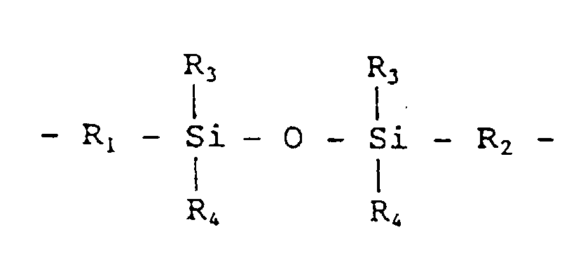
- Dispositif semi-conducteur selon la revendication 16, dans lequel la résine polybenzoxazole est obtenue en enduisant l'élément semi-conducteur avec une composition à base de résine photosensible de type positif qui comprend :(A) 100 parties en poids d'un polyamide représenté par la formule générale (1) définie dans la revendication 1,(B) 1 à 100 parties en poids d'un composé diazoquinone photosensible, et(C) 1 à 50 parties en poids d'au moins un élément choisi dans l'ensemble constitué des composés phénoliques représentés par les formules générales (2) et (3) définies dans la revendication 1,
puis en soumettant la pellicule de revêtement résultante à une pré-cuisson, en exposant et en développant le motif de celle-ci, et après cela en faisant durcir à chaud la pellicule de revêtement façonnée selon ce motif. - Dispositif semi-conducteur selon la revendication 17, dans lequel le composé phénolique (C) est au moins un élément choisi dans l'ensemble constitué des composés phénoliques représentés par les formules générales (4) et (5) définies dans la revendication 2.
- Dispositif semi-conducteur selon la revendication 17 ou 18, dans lequel le composé phénolique (C) comprend les composés phénoliques représentés par les formules structurelles (6) et (7) définies dans la revendication 3, seuls ou en mélange, dans une proportion d'au moins 50 % en poids du poids total des composés phénoliques (C).
- Dispositif semi-conducteur selon la revendication 16, dans lequel la résine polybenzoxazole est obtenue en enduisant l'élément semi-conducteur avec une composition à base de résine photosensible de type positif qui comprend :(A) 100 parties en poids d'un polyamide représenté par la formule générale (1) définie dans la revendication 1,(B) 1 à 100 parties en poids d'un composé diazoquinone photosensible, et(D) 0,1 à 20 parties en poids d'au moins un composé organosilicique choisi dans l'ensemble constitué des composés représentés par les formules générales (8), (9), et (10) définies dans la revendication 4, puis en soumettant la pellicule de revêtement résultante à une pré-cuisson, en exposant et en développant le motif de celle-ci, et après cela en faisant durcir à chaud la pellicule de revêtement façonnée selon ce motif.
- Dispositif semi-conducteur selon la revendication 20, dans lequel R18, dans la formule générale (8), est -CH=CH-.
- Dispositif semi-conducteur selon la revendication 20, dans lequel R22, dans la formule générale (9), est choisi dans l'ensemble constitué des groupes tétravalents représentés par les formules (11) suivantes :
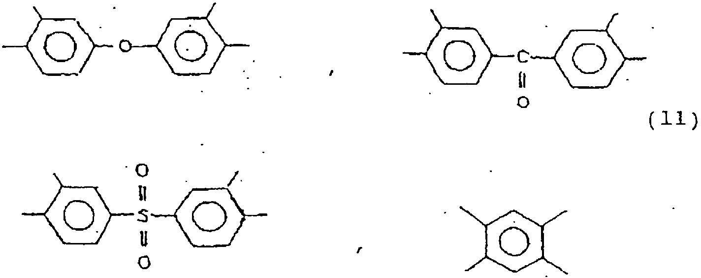
- Dispositif semi-conducteur selon la revendication 16, dans lequel la résine polybenzoxazole est obtenue en enduisant l'élément semi-conducteur avec une composition à base de résine photosensible de type positif qui comprend :(A) 100 parties en poids d'un polyamide représenté par la formule générale (1) définie dans la revendication 1,(B) 1 à 100 parties en poids d'un composé diazoquinone photosensible,(C) 1 à 50 parties en poids d'au moins un composé phénolique choisi dans l'ensemble constitué des composés représentés par les formules générales (2) et (3) définies dans la revendication 1, et(D) 0,1 à 20 parties en poids d'au moins un composé organosilicique choisi dans l'ensemble constitué des composés représentés par les formules générales (8), (9), et (10) définies dans la revendication 4,
puis en soumettant la pellicule de revêtement résultante à une pré-cuisson, en exposant et en développant le motif de celle-ci, et, après cela, en faisant durcir à chaud la pellicule de revêtement façonnée selon ce motif. - Dispositif semi-conducteur selon la revendication 23, dans lequel le composé phénolique (C) est au moins un élément choisi dans l'ensemble constitué des composés phénoliques représentés par les formules structurelles (4) et (5) définies dans la revendication 2.
- Dispositif semi-conducteur selon la revendication 23 ou 24, dans lequel le composé phénolique (C) comprend les composés phénoliques représentés par les formules structurelles (6) et (7) définies dans la revendication 3, seuls ou en mélange, dans une proportion d'au moins 50 % en poids du poids total de composés phénoliques (C).
- Dispositif semi-conducteur selon l'une quelconque des revendications 17 à 25, dans lequel X, dans la formule générale (1), est choisi dans l'ensemble constitué des groupes tétravalents représentés par les formules (12) définies dans la revendication 7.
- Dispositif semi-conducteur selon l'une quelconque des revendications 17 à 26, dans lequel Y, dans la formule générale (1), est choisi dans l'ensemble constitué des groupes divalents représentés par les formules (13) définies dans la revendication 8.
- Dispositif semi-conducteur selon l'une quelconque des revendications 17 à 27, dans lequel le composé diazoquinone photosensible (B) est choisi dans l'ensemble constitué des composés représentés par les formules générales (14) définies dans la revendication 9.
Applications Claiming Priority (15)
| Application Number | Priority Date | Filing Date | Title |
|---|---|---|---|
| JP117387/96 | 1996-05-13 | ||
| JP11738796A JP3207352B2 (ja) | 1996-05-13 | 1996-05-13 | ポジ型感光性樹脂組成物 |
| JP11738796 | 1996-05-13 | ||
| JP13859396A JP3346981B2 (ja) | 1996-05-31 | 1996-05-31 | 半導体装置 |
| JP138593/96 | 1996-05-31 | ||
| JP13859396 | 1996-05-31 | ||
| JP15967996A JP3449856B2 (ja) | 1996-06-20 | 1996-06-20 | ポジ型感光性樹脂組成物 |
| JP15967996 | 1996-06-20 | ||
| JP159679/96 | 1996-06-20 | ||
| JP164472/96 | 1996-06-25 | ||
| JP16447296 | 1996-06-25 | ||
| JP16447296A JP3449858B2 (ja) | 1996-06-25 | 1996-06-25 | ポジ型感光性樹脂組成物 |
| JP169319/96 | 1996-06-28 | ||
| JP16931996A JP3390303B2 (ja) | 1996-06-28 | 1996-06-28 | 半導体装置 |
| JP16931996 | 1996-06-28 |
Publications (2)
| Publication Number | Publication Date |
|---|---|
| EP0807852A1 EP0807852A1 (fr) | 1997-11-19 |
| EP0807852B1 true EP0807852B1 (fr) | 2001-03-21 |
Family
ID=27526762
Family Applications (1)
| Application Number | Title | Priority Date | Filing Date |
|---|---|---|---|
| EP97107190A Expired - Lifetime EP0807852B1 (fr) | 1996-05-13 | 1997-04-30 | Composition à base de résine photosensible, de type positif et dispositif semi-conducteur utilisant celle-ci |
Country Status (6)
| Country | Link |
|---|---|
| US (2) | US6071666A (fr) |
| EP (1) | EP0807852B1 (fr) |
| KR (1) | KR100533488B1 (fr) |
| CN (2) | CN1113273C (fr) |
| DE (1) | DE69704294T2 (fr) |
| TW (1) | TW502135B (fr) |
Cited By (3)
| Publication number | Priority date | Publication date | Assignee | Title |
|---|---|---|---|---|
| DE10137376A1 (de) * | 2001-07-31 | 2003-02-27 | Infineon Technologies Ag | Geklebte Chip- und Waferstapel |
| DE10137375A1 (de) * | 2001-07-31 | 2003-02-27 | Infineon Technologies Ag | Verwendung von Polybenzoxazolen (PBO) zum Kleben |
| TWI490652B (zh) * | 2008-05-07 | 2015-07-01 | Sumitomo Bakelite Co | 正型感光性樹脂組成物,硬化膜,保護膜及絕緣膜,暨利用其等之半導體裝置及顯示體裝置 |
Families Citing this family (46)
| Publication number | Priority date | Publication date | Assignee | Title |
|---|---|---|---|---|
| JP3509612B2 (ja) * | 1998-05-29 | 2004-03-22 | 日立化成デュポンマイクロシステムズ株式会社 | 感光性重合体組成物、レリーフパターンの製造法及び電子部品 |
| US6214516B1 (en) * | 1998-10-01 | 2001-04-10 | Arch Specialty Chemicals, Inc. | Photosensitive resin compositions |
| JP3426531B2 (ja) * | 1998-10-30 | 2003-07-14 | 日立化成デュポンマイクロシステムズ株式会社 | 感光性重合体組成物、レリーフパターンの製造法及び電子部品 |
| JP3667184B2 (ja) * | 1999-02-26 | 2005-07-06 | 住友ベークライト株式会社 | 半導体装置 |
| EP1132773B1 (fr) * | 1999-06-01 | 2007-07-11 | Toray Industries, Inc. | Composition de precurseur de polyimide photosensible de type positif |
| JP2002040654A (ja) * | 2000-07-31 | 2002-02-06 | Sumitomo Bakelite Co Ltd | ポジ型感光性樹脂組成物 |
| DE60142844D1 (de) * | 2000-10-31 | 2010-09-30 | Intel Corp | Positive lichtempfindliche harzzusammensetzung, prozess zu ihrer herstellung und halbleiterbauelemente |
| JP4371587B2 (ja) * | 2001-01-05 | 2009-11-25 | 住友ベークライト株式会社 | 半導体装置の製造方法 |
| KR100830773B1 (ko) * | 2001-05-07 | 2008-05-20 | 스미토모 베이클리트 컴퍼니 리미티드 | 포지티브형 감광성 수지 조성물 및 반도체 장치 |
| JP4084597B2 (ja) * | 2002-05-07 | 2008-04-30 | 群栄化学工業株式会社 | アミノ基含有フェノール誘導体 |
| US7214455B2 (en) * | 2002-05-29 | 2007-05-08 | Toray Industries, Inc. | Photosensitive resin composition and process for producing heat-resistant resin film |
| DE10228769A1 (de) * | 2002-06-27 | 2004-02-05 | Infineon Technologies Ag | Isoliermaterial für Aluminium und Kupfermetallisierungen |
| US6887643B2 (en) * | 2002-08-05 | 2005-05-03 | Toray Industries, Inc. | Photosensitive resin precursor composition |
| KR20060002768A (ko) * | 2003-03-11 | 2006-01-09 | 후지필름 일렉트로닉 머티리얼스 유.에스.에이., 아이엔씨. | 새로운 감광성 수지 조성물들 |
| WO2004109400A2 (fr) * | 2003-03-11 | 2004-12-16 | Arch Speciality Chemicals, Inc. | Nouvelles compositions de resine photosensible |
| EP1606326A2 (fr) * | 2003-03-11 | 2005-12-21 | FujiFilm Electronic Materials USA, Inc. | Compositions de resine photosensibles |
| EP1491952B1 (fr) * | 2003-06-23 | 2015-10-07 | Sumitomo Bakelite Co., Ltd. | Composition à base de résine photosensible de type positif, procédé de fabrication d'un film de résine à motifs, dispositif semi-conducteur, dispositif d'affichage, et procédé de fabrication de ces derniers |
| TW200512543A (en) | 2003-08-06 | 2005-04-01 | Sumitomo Bakelite Co | Polyamide resin, positive-working photosensitive resin composition, method for producing pattern-formed resin film, semiconductor device, display device, and method for producing the semiconductor device and the display device |
| US7416822B2 (en) * | 2004-01-20 | 2008-08-26 | Asahi Kasei Emd Corporation | Resin and resin composition |
| US7435525B2 (en) * | 2004-05-07 | 2008-10-14 | Hitachi Chemical Dupont Microsystems Ltd. | Positive photosensitive resin composition, method for forming pattern, and electronic part |
| WO2006044338A1 (fr) * | 2004-10-13 | 2006-04-27 | Dow Global Technologies Inc. | Formule de polymère de benzocylclobutène hydroexpansible et méthode d’utilisation de telles formules |
| US7795462B2 (en) | 2005-01-13 | 2010-09-14 | Xerox Corporation | Crosslinked siloxane outmost layer having aromatic silicon-containing compounds for photoreceptors |
| TW200702913A (en) * | 2005-06-03 | 2007-01-16 | Fujifilm Electronic Materials | Pretreatment compositions |
| KR100669508B1 (ko) * | 2005-08-31 | 2007-01-16 | 한국화학연구원 | 아믹산-실록산 화합물과 이 화합물을 졸-겔 반응하여제조된 이미드-실록산 중합체 |
| WO2007063721A1 (fr) * | 2005-11-30 | 2007-06-07 | Sumitomo Bakelite Co., Ltd. | Composition de resine photosensible positive et dispositif semi-conducteur et ecran l’utilisant |
| JP2007240975A (ja) * | 2006-03-09 | 2007-09-20 | Fujifilm Corp | 感光性樹脂組成物及びそれを用いた半導体装置の製造方法 |
| WO2008020573A1 (fr) * | 2006-08-15 | 2008-02-21 | Asahi Kasei Emd Corporation | Composition de résine photosensible positive |
| TWI397770B (zh) * | 2006-08-17 | 2013-06-01 | Hitachi Chem Dupont Microsys | 正型光阻組成物、圖案的製造方法以及電子零件 |
| US8269358B2 (en) | 2006-10-24 | 2012-09-18 | Sumitomo Bakelite Company Limited | Bis(aminophenol) derivative, process for producing same, polyamide resin, positive photosensitive resin composition, protective film, interlayer dielectric film, semiconductor device, and display element |
| US20100009290A1 (en) * | 2006-12-03 | 2010-01-14 | Central Glass Co., Ltd. | Photosensitive Polybenzoxazines and Methods of Making the Same |
| US20100216070A1 (en) * | 2006-12-04 | 2010-08-26 | Central Glass Co., Ltd. | Photosensitive Polyimides and Methods of Making the Same |
| US7678514B2 (en) * | 2007-12-27 | 2010-03-16 | Sumitomo Bakelite Co., Ltd. | Positive-type photosensitive resin composition, cured film, protecting film, insulating film and semiconductor device and display device using these films |
| KR100995079B1 (ko) | 2008-09-29 | 2010-11-18 | 제일모직주식회사 | 포지티브형 감광성 수지 조성물 |
| JP5410918B2 (ja) * | 2008-10-20 | 2014-02-05 | チェイル インダストリーズ インコーポレイテッド | ポジティブ型感光性樹脂組成物 |
| US8530119B2 (en) * | 2009-05-20 | 2013-09-10 | Sumitomo Bakelite Co., Ltd. | Positive photosensitive resin composition, cured film, protective film, interlayer insulating film, and semiconductor device and display element using the same |
| KR101354640B1 (ko) * | 2011-12-30 | 2014-01-27 | 제일모직주식회사 | 포지티브형 감광성 수지 조성물 |
| TW201525064A (zh) * | 2013-12-16 | 2015-07-01 | Daxin Materials Corp | 感光樹脂組成物、感光樹脂及有機發光二極體顯示元件 |
| CN109563353B (zh) * | 2016-07-27 | 2022-01-14 | 东丽株式会社 | 树脂组合物 |
| JP6637871B2 (ja) | 2016-10-27 | 2020-01-29 | 信越化学工業株式会社 | テトラカルボン酸ジエステル化合物、ポリイミド前駆体の重合体及びその製造方法、ネガ型感光性樹脂組成物、パターン形成方法、及び硬化被膜形成方法 |
| KR102341494B1 (ko) * | 2016-11-02 | 2021-12-23 | 도레이 카부시키가이샤 | 수지 조성물, 수지 시트, 경화막, 유기 el 표시 장치, 반도체 전자 부품, 반도체 장치 및 유기 el 표시 장치의 제조 방법 |
| EP3616903B1 (fr) * | 2017-04-28 | 2023-09-27 | Mitsui Chemicals, Inc. | Corps stratifié et méthode de fabrication d'un corps stratifié |
| US11634529B2 (en) | 2017-06-16 | 2023-04-25 | Fujifilm Electronic Materials U.S.A., Inc. | Multilayer structure |
| KR102331157B1 (ko) * | 2019-10-23 | 2021-11-26 | (주)휴넷플러스 | 폴리실록산 공중합체, 이의 제조방법 및 이를 포함하는 수지 조성물 |
| CN111019345B (zh) * | 2019-12-17 | 2021-06-29 | 中国科学院化学研究所 | 一种聚(酰亚胺-苯并噁唑)薄膜及其制备方法与用途 |
| CN111518272B (zh) * | 2020-04-20 | 2023-11-28 | Tcl华星光电技术有限公司 | 显示面板 |
| WO2022163673A1 (fr) * | 2021-01-27 | 2022-08-04 | 日産化学株式会社 | Composition de formation de film de sous-couche de réserve contenant un produit de réaction de dianhydride d'acide |
Family Cites Families (27)
| Publication number | Priority date | Publication date | Assignee | Title |
|---|---|---|---|---|
| NL95406C (fr) * | 1954-08-20 | |||
| BE540225A (fr) * | 1954-08-20 | |||
| US3755354A (en) * | 1969-05-05 | 1973-08-28 | Gen Electric | Amide acid and imido-substituted organosilanes |
| US3669658A (en) * | 1969-06-11 | 1972-06-13 | Fuji Photo Film Co Ltd | Photosensitive printing plate |
| JPS6036571B2 (ja) * | 1978-06-14 | 1985-08-21 | 株式会社日立製作所 | 液晶表示セル |
| DE2931297A1 (de) * | 1979-08-01 | 1981-02-19 | Siemens Ag | Waermebestaendige positivresists und verfahren zur herstellung waermebestaendiger reliefstrukturen |
| US4460739A (en) * | 1983-07-01 | 1984-07-17 | General Electric Company | Composition for promoting adhesion of curable silicones to substrates |
| EP0291779B1 (fr) * | 1987-05-18 | 1994-07-27 | Siemens Aktiengesellschaft | Réserves positives résistantes à la chaleur et procédé de fabrication de structures formant réserve résistantes à la chaleur |
| US4927736A (en) * | 1987-07-21 | 1990-05-22 | Hoechst Celanese Corporation | Hydroxy polyimides and high temperature positive photoresists therefrom |
| JPS6446862A (en) * | 1987-08-18 | 1989-02-21 | Fujitsu Ltd | Bus controller |
| JPH0830167B2 (ja) * | 1988-02-24 | 1996-03-27 | 日本合成ゴム株式会社 | 硬化性組成物 |
| DE3837612A1 (de) * | 1988-11-05 | 1990-05-23 | Ciba Geigy Ag | Positiv-fotoresists von polyimid-typ |
| US5288588A (en) * | 1989-10-27 | 1994-02-22 | Nissan Chemical Industries Ltd. | Positive photosensitive polyimide resin composition comprising an o-quinone diazide as a photosensitive compound |
| JP2566169B2 (ja) * | 1989-12-28 | 1996-12-25 | 日本ゼオン株式会社 | ポジ型レジスト組成物 |
| JP2566171B2 (ja) * | 1989-12-28 | 1996-12-25 | 日本ゼオン株式会社 | ポジ型レジスト組成物 |
| JPH087435B2 (ja) * | 1989-12-28 | 1996-01-29 | 日本ゼオン株式会社 | ポジ型レジスト組成物 |
| JPH061377B2 (ja) * | 1989-12-28 | 1994-01-05 | 日本ゼオン株式会社 | ポジ型レジスト組成物 |
| JP2764220B2 (ja) | 1990-04-27 | 1998-06-11 | パイオニア株式会社 | オーディオディスク・メモリディスク兼用ディスクプレーヤ |
| JPH041651A (ja) * | 1990-04-18 | 1992-01-07 | Nippon Zeon Co Ltd | ポジ型レジスト組成物 |
| JP2694472B2 (ja) * | 1990-04-18 | 1997-12-24 | 日本ゼオン株式会社 | ポジ型レジスト組成物 |
| JPH0411260A (ja) * | 1990-04-27 | 1992-01-16 | Toray Ind Inc | ポジ型フォトレジスト組成物 |
| JPH0412356A (ja) * | 1990-04-28 | 1992-01-16 | Toray Ind Inc | ポジ型フォトレジスト組成物 |
| JP2629403B2 (ja) * | 1990-04-28 | 1997-07-09 | 東レ株式会社 | ポジ型フォトレジスト組成物 |
| EP0459395B1 (fr) * | 1990-05-29 | 1999-08-18 | Sumitomo Bakelite Company Limited | Composition résineuse photosensible positive |
| JP2806622B2 (ja) * | 1990-10-25 | 1998-09-30 | 日本電気株式会社 | ヒートシンクの取付構造 |
| KR0134753B1 (ko) * | 1993-02-26 | 1998-04-18 | 사토 후미오 | 폴리아미드산 조성물 |
| JP3078175B2 (ja) * | 1994-05-06 | 2000-08-21 | 住友ベークライト株式会社 | 感光性樹脂組成物 |
-
1997
- 1997-04-29 TW TW086105647A patent/TW502135B/zh not_active IP Right Cessation
- 1997-04-30 EP EP97107190A patent/EP0807852B1/fr not_active Expired - Lifetime
- 1997-04-30 DE DE69704294T patent/DE69704294T2/de not_active Expired - Lifetime
- 1997-05-12 CN CN97111184A patent/CN1113273C/zh not_active Expired - Fee Related
- 1997-05-12 KR KR1019970018351A patent/KR100533488B1/ko not_active Expired - Lifetime
- 1997-05-12 US US08/854,863 patent/US6071666A/en not_active Expired - Lifetime
-
1999
- 1999-11-17 US US09/442,277 patent/US6235436B1/en not_active Expired - Lifetime
-
2002
- 2002-04-29 CN CNB021190453A patent/CN1215380C/zh not_active Expired - Fee Related
Cited By (5)
| Publication number | Priority date | Publication date | Assignee | Title |
|---|---|---|---|---|
| DE10137376A1 (de) * | 2001-07-31 | 2003-02-27 | Infineon Technologies Ag | Geklebte Chip- und Waferstapel |
| DE10137375A1 (de) * | 2001-07-31 | 2003-02-27 | Infineon Technologies Ag | Verwendung von Polybenzoxazolen (PBO) zum Kleben |
| US6787244B2 (en) | 2001-07-31 | 2004-09-07 | Infineon Technologies Ag | Adhesively bonded chip-and wafer stacks |
| US7052936B2 (en) | 2001-07-31 | 2006-05-30 | Infineon Technologies Ag | Use of polybenzoxazoles (PBOS) for adhesion |
| TWI490652B (zh) * | 2008-05-07 | 2015-07-01 | Sumitomo Bakelite Co | 正型感光性樹脂組成物,硬化膜,保護膜及絕緣膜,暨利用其等之半導體裝置及顯示體裝置 |
Also Published As
| Publication number | Publication date |
|---|---|
| DE69704294T2 (de) | 2001-09-13 |
| KR970076084A (ko) | 1997-12-10 |
| KR100533488B1 (ko) | 2006-04-14 |
| US6235436B1 (en) | 2001-05-22 |
| CN1165980A (zh) | 1997-11-26 |
| TW502135B (en) | 2002-09-11 |
| CN1113273C (zh) | 2003-07-02 |
| CN1381768A (zh) | 2002-11-27 |
| DE69704294D1 (de) | 2001-04-26 |
| CN1215380C (zh) | 2005-08-17 |
| EP0807852A1 (fr) | 1997-11-19 |
| US6071666A (en) | 2000-06-06 |
Similar Documents
| Publication | Publication Date | Title |
|---|---|---|
| EP0807852B1 (fr) | Composition à base de résine photosensible, de type positif et dispositif semi-conducteur utilisant celle-ci | |
| JP3207352B2 (ja) | ポジ型感光性樹脂組成物 | |
| JP3478376B2 (ja) | ポジ型感光性樹脂組成物 | |
| JP3995962B2 (ja) | ポジ型感光性樹脂組成物及び半導体装置 | |
| US5587275A (en) | Photosensitive resin composition and a process for forming a patterned polyimide film using the same | |
| JP3449925B2 (ja) | ポジ型感光性樹脂組成物 | |
| JP3078175B2 (ja) | 感光性樹脂組成物 | |
| EP1400849B1 (fr) | Compositions de resine photosensibles positives et dispositif a semi-conducteur | |
| JP3422691B2 (ja) | ポジ型感光性樹脂組成物 | |
| JPH11312675A (ja) | 半導体装置及びその製造方法 | |
| JP4206709B2 (ja) | ポジ型感光性樹脂組成物及び半導体装置 | |
| JP2002040654A (ja) | ポジ型感光性樹脂組成物 | |
| JP3390303B2 (ja) | 半導体装置 | |
| JP3422703B2 (ja) | ポジ型感光性樹脂組成物及びそれを用いた半導体装置 | |
| JP4040216B2 (ja) | ポジ型感光性樹脂組成物及びそれを用いた半導体装置 | |
| JP3449926B2 (ja) | ポジ型感光性樹脂組成物 | |
| JP3422704B2 (ja) | ポジ型感光性樹脂組成物 | |
| JP3449858B2 (ja) | ポジ型感光性樹脂組成物 | |
| JP3737342B2 (ja) | ポリアミド樹脂、ポジ型感光性樹脂組成物及び半導体装置 | |
| JP4325159B2 (ja) | ナフトキノンジアジドスルホン酸エステル、それを用いたポジ型感光性樹脂組成物及び半導体装置 | |
| JP2000131845A (ja) | ポジ型感光性樹脂組成物、およびそれを用いた半導体装置 | |
| JP3844106B2 (ja) | ポジ型感光性樹脂組成物の硬化方法及びその方法により製作された半導体装置 | |
| JP3449856B2 (ja) | ポジ型感光性樹脂組成物 | |
| JP2002241611A (ja) | ポジ型感光性樹脂組成物及び半導体装置 | |
| JP4348846B2 (ja) | 有機層の形成方法 |
Legal Events
| Date | Code | Title | Description |
|---|---|---|---|
| PUAI | Public reference made under article 153(3) epc to a published international application that has entered the european phase |
Free format text: ORIGINAL CODE: 0009012 |
|
| AK | Designated contracting states |
Kind code of ref document: A1 Designated state(s): DE FR GB IT NL |
|
| 17P | Request for examination filed |
Effective date: 19980403 |
|
| 17Q | First examination report despatched |
Effective date: 19990217 |
|
| GRAG | Despatch of communication of intention to grant |
Free format text: ORIGINAL CODE: EPIDOS AGRA |
|
| GRAG | Despatch of communication of intention to grant |
Free format text: ORIGINAL CODE: EPIDOS AGRA |
|
| GRAG | Despatch of communication of intention to grant |
Free format text: ORIGINAL CODE: EPIDOS AGRA |
|
| GRAH | Despatch of communication of intention to grant a patent |
Free format text: ORIGINAL CODE: EPIDOS IGRA |
|
| GRAH | Despatch of communication of intention to grant a patent |
Free format text: ORIGINAL CODE: EPIDOS IGRA |
|
| GRAA | (expected) grant |
Free format text: ORIGINAL CODE: 0009210 |
|
| ITF | It: translation for a ep patent filed | ||
| AK | Designated contracting states |
Kind code of ref document: B1 Designated state(s): DE FR GB IT NL |
|
| REF | Corresponds to: |
Ref document number: 69704294 Country of ref document: DE Date of ref document: 20010426 |
|
| ET | Fr: translation filed | ||
| REG | Reference to a national code |
Ref country code: GB Ref legal event code: IF02 |
|
| PLBE | No opposition filed within time limit |
Free format text: ORIGINAL CODE: 0009261 |
|
| STAA | Information on the status of an ep patent application or granted ep patent |
Free format text: STATUS: NO OPPOSITION FILED WITHIN TIME LIMIT |
|
| 26N | No opposition filed | ||
| PGFP | Annual fee paid to national office [announced via postgrant information from national office to epo] |
Ref country code: GB Payment date: 20140430 Year of fee payment: 18 |
|
| PGFP | Annual fee paid to national office [announced via postgrant information from national office to epo] |
Ref country code: IT Payment date: 20140415 Year of fee payment: 18 Ref country code: NL Payment date: 20140308 Year of fee payment: 18 Ref country code: DE Payment date: 20140430 Year of fee payment: 18 Ref country code: FR Payment date: 20140409 Year of fee payment: 18 |
|
| REG | Reference to a national code |
Ref country code: DE Ref legal event code: R119 Ref document number: 69704294 Country of ref document: DE |
|
| GBPC | Gb: european patent ceased through non-payment of renewal fee |
Effective date: 20150430 |
|
| REG | Reference to a national code |
Ref country code: NL Ref legal event code: MM Effective date: 20150501 |
|
| PG25 | Lapsed in a contracting state [announced via postgrant information from national office to epo] |
Ref country code: IT Free format text: LAPSE BECAUSE OF NON-PAYMENT OF DUE FEES Effective date: 20150430 Ref country code: GB Free format text: LAPSE BECAUSE OF NON-PAYMENT OF DUE FEES Effective date: 20150430 Ref country code: DE Free format text: LAPSE BECAUSE OF NON-PAYMENT OF DUE FEES Effective date: 20151103 |
|
| REG | Reference to a national code |
Ref country code: FR Ref legal event code: ST Effective date: 20151231 |
|
| PG25 | Lapsed in a contracting state [announced via postgrant information from national office to epo] |
Ref country code: FR Free format text: LAPSE BECAUSE OF NON-PAYMENT OF DUE FEES Effective date: 20150430 |
|
| PG25 | Lapsed in a contracting state [announced via postgrant information from national office to epo] |
Ref country code: NL Free format text: LAPSE BECAUSE OF NON-PAYMENT OF DUE FEES Effective date: 20150501 |