EP0809100A1 - Capteur pour la détection des fluides et méthode de production - Google Patents
Capteur pour la détection des fluides et méthode de production Download PDFInfo
- Publication number
- EP0809100A1 EP0809100A1 EP97107121A EP97107121A EP0809100A1 EP 0809100 A1 EP0809100 A1 EP 0809100A1 EP 97107121 A EP97107121 A EP 97107121A EP 97107121 A EP97107121 A EP 97107121A EP 0809100 A1 EP0809100 A1 EP 0809100A1
- Authority
- EP
- European Patent Office
- Prior art keywords
- substrate
- sensor
- sensor element
- element according
- sensor layer
- Prior art date
- Legal status (The legal status is an assumption and is not a legal conclusion. Google has not performed a legal analysis and makes no representation as to the accuracy of the status listed.)
- Granted
Links
Images
Classifications
-
- G—PHYSICS
- G01—MEASURING; TESTING
- G01N—INVESTIGATING OR ANALYSING MATERIALS BY DETERMINING THEIR CHEMICAL OR PHYSICAL PROPERTIES
- G01N27/00—Investigating or analysing materials by the use of electric, electrochemical, or magnetic means
- G01N27/02—Investigating or analysing materials by the use of electric, electrochemical, or magnetic means by investigating impedance
- G01N27/04—Investigating or analysing materials by the use of electric, electrochemical, or magnetic means by investigating impedance by investigating resistance
- G01N27/12—Investigating or analysing materials by the use of electric, electrochemical, or magnetic means by investigating impedance by investigating resistance of a solid body in dependence upon absorption of a fluid; of a solid body in dependence upon reaction with a fluid, for detecting components in the fluid
Definitions
- the invention relates to a sensor element for the detection of liquid, gaseous or fluid substances with a sensor layer formed on a substrate as well as a manufacturing method of such a sensor element.
- the sensor layer is the layer with which the substance to be measured is converted into a measurable sensor signal.
- the sensor layer can consist of a coherent layer of a suitable material, for example tin oxide, or can comprise interdigital capacitor structures, gate regions of field effect transistors, Hall structures etc.
- Such a sensor element and such a manufacturing method are known from practice.
- the electrical contacting of the sensor element leads to a number of difficulties.
- the sensor layer must be connected to external electrical contacts in order to record measured values of the sensor element.
- This connection is usually made using bond wires.
- bond pads are arranged at a spatially very small distance from the sensor surface. As a rule, this leads to bond pads and bond wires coming into contact with the substance to be detected during the measurement process. This significantly affects the reliability of the bond connections.
- the bond pads require additional area of the sensor layer, since a reaction of the sensor layer due to the substance to be detected is prevented at the point at which the bond wire is attached.
- the heater would reduce the reliability of the bond connection.
- the measuring accuracy of the sensor element can be impaired by the fact that a part of the substance to be detected that does not contribute to the reaction with the sensor surface leads to reactions with the bonding wire that significantly impair the measuring accuracy.
- the production of such sensor elements is also costly since the sensor elements have to be attached to special chip carriers (lead frames), and so on the assembly technology is complex because individual sensor elements have to be handled in order to carry out various process steps.
- the invention has for its object to provide a reliable, simple and inexpensive generic sensor element.
- a generic sensor element in which a signal line device for conducting a sensor signal is arranged in the substrate in such a way that it connects the back of the sensor layer facing the substrate to the back of the substrate or at least one side of the substrate.
- the object is achieved by a production method in which a signal line device for conducting a sensor signal is arranged in the substrate in such a way that it connects the back side of the sensor layer facing the substrate to the back side of the substrate or to a side surface of the substrate.
- the signal line device Due to the arrangement of the signal line device according to the invention, no electrical contacts in the form of bond pads and bond wires are required on the front side of the sensor layer to which the substance to be measured is applied. In this way, an impairment of the measuring accuracy of the sensor element, as can occur due to the above-mentioned bond connections, is completely excluded.
- the sensor layer and thus also the sensor element can be smaller be formed since no additional space is required to apply bond pads. This contributes significantly to the cost reduction, in particular if an expensive material is used for the substrate. In addition, smaller and smaller sensors are also desirable for many applications, since this can save space.
- the reliability of the signal line device is also not impaired by heating the sensor, since the heater can be attached to another location in the substrate.
- such a sensor is also cheaper in that no additional chip carrier is required, since the contact can be made directly on the back of the substrate or on the substrate side surface (s). Interaction of the substance to be measured with the signal line device is also reliably prevented since it runs in the substrate.
- the signal line device comprises line-shaped cavities for receiving signal lines, which extend from the back of the sensor layer to the back of the substrate or the substrate side surface (s).
- the cavities can be filled with a metal. This enables a simple, reliable, electrical connection between the sensor surface and external electrical contacts.
- the sensor element can be further simplified in that contact pins are inserted directly into the metal in the cavities, with which contact pins the sensor element can be inserted, for example, into a circuit board.
- the cavities are particularly easy to produce if they extend in a line from the back of the sensor layer to the back of the substrate.
- a protective device which delimits the side surface of the substrate and projects beyond the sensor layer is formed.
- the area in which the substance to be detected can spread is spatially limited.
- the substance is prevented from reaching the contacts outside the substrate.
- the protective device against the substance is expediently sealed on the side surfaces educated. This ensures that the entire substance used remains on the surface of the substrate. Even small amounts are prevented from reaching the side surface or the back of the substrate and thus the electrical contacts. As a result, a smaller part of the substance is required.
- the sensor layer extends essentially over the entire cross section of the substrate.
- the upper end of the protective device can be provided with a connection device. Then it is particularly easy to add the substance in a targeted manner. The substance can be added without losses.
- a discharge device for the portion of the substance which is not used for detection and for the reaction on the sensor surface can also be arranged in the connection device.
- the substrate is a semiconductor substrate.
- the substrate is a glass substrate.
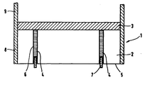
- FIG. 1 shows a sensor element according to the invention in cross section.
- the sensor element 1 has a substrate 2, on the front of which a sensor layer 3 is applied.
- the sensor layer 3 covers the entire cross section of the substrate 1.
- Two signal lines 4 are arranged in the substrate 2 in such a way that they connect the rear side of the sensor layer 3 facing the substrate 1 to the substrate rear side 5.
- the signal lines 4 lie in line-shaped, here cylindrical, cavities 6 and consist of a metal with which the cavities 6 are filled.
- Contact pins 7 are introduced into the cavities 6 from the substrate rear side 5 and are firmly connected to the metal present in the cavities 6.
- the substrate 2 and the sensor layer 3 are surrounded by a protective device 8, which is formed on the side surfaces of the substrate, preferably sealing against the substance.
- the protective device 8 stands above the surface of the Sensor layer 3 over.
- the length of the protruding part 9 of the protective device 8 above the sensor layer 3 is selected depending on the substance to be measured. It is essential that the substance to be measured is prevented from reaching the rear of the sensor element 1, where the electrical contacts, here the contact styles 7, are located.
- the protruding part 9 of the protective device 8 can be provided with a connection device to which devices for supplying or discharging the substance to be measured, such as pumps, valves etc., can be connected.
- the sensor layer 3 is applied to the substrate 2 in a conventional manner.
- the back of the body is thinned if necessary and further suitable method steps are carried out.
- the cavities 6 are formed in the sensor elements 1 and filled with a suitable metal.
- the contact pins 7 are attached to the signal lines 4, for example by soldering, welding, gluing, etc.
- the sensor elements 1 are separated from each other.
- the protective device 8 is then applied to the side surfaces of the individually present sensor elements.
- the protective device 8 can be, for example, a shrink tube, which is attached to the substance in a sealing manner by heat treatment on the side surfaces of the substrate 2.
- the protective device 8 can also be produced, for example, by an interference fit of a metal.
Landscapes
- Chemical & Material Sciences (AREA)
- Chemical Kinetics & Catalysis (AREA)
- Electrochemistry (AREA)
- Physics & Mathematics (AREA)
- Health & Medical Sciences (AREA)
- Life Sciences & Earth Sciences (AREA)
- Analytical Chemistry (AREA)
- Biochemistry (AREA)
- General Health & Medical Sciences (AREA)
- General Physics & Mathematics (AREA)
- Immunology (AREA)
- Pathology (AREA)
- Investigating Or Analyzing Materials By The Use Of Fluid Adsorption Or Reactions (AREA)
- Investigating Or Analyzing Materials By The Use Of Electric Means (AREA)
Applications Claiming Priority (2)
| Application Number | Priority Date | Filing Date | Title |
|---|---|---|---|
| DE19621227A DE19621227C2 (de) | 1996-05-25 | 1996-05-25 | Sensorelement zum Nachweis von flüssigen, gasförmigen oder fluiden Substanzen |
| DE19621227 | 1996-05-25 |
Publications (2)
| Publication Number | Publication Date |
|---|---|
| EP0809100A1 true EP0809100A1 (fr) | 1997-11-26 |
| EP0809100B1 EP0809100B1 (fr) | 2004-11-17 |
Family
ID=7795391
Family Applications (1)
| Application Number | Title | Priority Date | Filing Date |
|---|---|---|---|
| EP97107121A Expired - Lifetime EP0809100B1 (fr) | 1996-05-25 | 1997-04-29 | Capteur pour la détection des fluides et méthode de production |
Country Status (3)
| Country | Link |
|---|---|
| EP (1) | EP0809100B1 (fr) |
| JP (1) | JPH10132772A (fr) |
| DE (2) | DE19621227C2 (fr) |
Families Citing this family (3)
| Publication number | Priority date | Publication date | Assignee | Title |
|---|---|---|---|---|
| EP1189281B1 (fr) * | 1998-06-30 | 2007-08-22 | Micronas GmbH | Agencement de puce électronique |
| DE10156227C1 (de) * | 2001-11-15 | 2003-05-28 | Schott Glas | pH-Einstabmeßkette mit einem Diaphragma-Verschluß |
| DE102007036473A1 (de) * | 2007-08-01 | 2009-02-05 | Testo Ag | Vorrichtung zum Messen des Zustands eines Messguts, insbesondere von Ölen oder Fetten |
Citations (3)
| Publication number | Priority date | Publication date | Assignee | Title |
|---|---|---|---|---|
| US4151503A (en) * | 1977-10-05 | 1979-04-24 | Ford Motor Company | Temperature compensated resistive exhaust gas sensor construction |
| US5417100A (en) * | 1993-03-10 | 1995-05-23 | Hughes Aircraft Company | Reversible sensor for detecting solvent vapors |
| US5511428A (en) * | 1994-06-10 | 1996-04-30 | Massachusetts Institute Of Technology | Backside contact of sensor microstructures |
Family Cites Families (6)
| Publication number | Priority date | Publication date | Assignee | Title |
|---|---|---|---|---|
| JPH02269947A (ja) * | 1989-04-11 | 1990-11-05 | Matsushita Electric Ind Co Ltd | 燃焼制御用センサ |
| DE4013593A1 (de) * | 1990-04-27 | 1991-10-31 | Biotechnolog Forschung Gmbh | Verfahren und sensor fuer amperometrische messprinzipien mit dickschicht-biosensoren |
| US5391272A (en) * | 1992-03-06 | 1995-02-21 | Andcare, Inc. | Electrochemical immunoassay methods |
| DE4230602C2 (de) * | 1992-09-12 | 1995-04-20 | Draegerwerk Ag | Elektrochemischer Sensor mit modularem Aufbau |
| US5284566A (en) * | 1993-01-04 | 1994-02-08 | Bacharach, Inc. | Electrochemical gas sensor with wraparound reference electrode |
| US5540086A (en) * | 1994-08-30 | 1996-07-30 | Kavlico Corporation | Oil deterioration sensor |
-
1996
- 1996-05-25 DE DE19621227A patent/DE19621227C2/de not_active Expired - Fee Related
-
1997
- 1997-04-29 EP EP97107121A patent/EP0809100B1/fr not_active Expired - Lifetime
- 1997-04-29 DE DE59712078T patent/DE59712078D1/de not_active Expired - Fee Related
- 1997-05-26 JP JP9135625A patent/JPH10132772A/ja active Pending
Patent Citations (3)
| Publication number | Priority date | Publication date | Assignee | Title |
|---|---|---|---|---|
| US4151503A (en) * | 1977-10-05 | 1979-04-24 | Ford Motor Company | Temperature compensated resistive exhaust gas sensor construction |
| US5417100A (en) * | 1993-03-10 | 1995-05-23 | Hughes Aircraft Company | Reversible sensor for detecting solvent vapors |
| US5511428A (en) * | 1994-06-10 | 1996-04-30 | Massachusetts Institute Of Technology | Backside contact of sensor microstructures |
Also Published As
| Publication number | Publication date |
|---|---|
| JPH10132772A (ja) | 1998-05-22 |
| DE19621227C2 (de) | 2003-02-20 |
| DE59712078D1 (de) | 2004-12-23 |
| EP0809100B1 (fr) | 2004-11-17 |
| DE19621227A1 (de) | 1997-11-27 |
Similar Documents
| Publication | Publication Date | Title |
|---|---|---|
| DE10141259B4 (de) | Drucksensor mit einem Halbleitersensorchip | |
| EP1182432B1 (fr) | Capteur de débit avec boîtier | |
| DE8407322U1 (de) | Piezoresestive druckmesszelle | |
| DE10228000A1 (de) | Vorrichtung zur Druckmessung | |
| EP0189492B1 (fr) | Méthode de fabrication d'un transducteur de mesure pour mesurer des grandeurs mécaniques | |
| DE69936199T2 (de) | Sensorpackung mit einer integrierten pfropfenelektrode | |
| DE19827237A1 (de) | Substrat für Halbleiterbauelementgehäuse und Halbleiterbauelementgehäuse unter Verwenden desselben, sowie Herstellungsverfahren für diese | |
| EP1682882A1 (fr) | Ensemble de detection comportant plusieurs capteurs potentiometriques | |
| DE102004059397A1 (de) | Drucksensor mit gekapselter Membran | |
| EP1917509A1 (fr) | Dispositif de detection comportant un substrat et un boitier et procede de fabrication d'un dispositif de detection | |
| DE69737320T2 (de) | Halbleitervorrichtung | |
| DE4201634C2 (de) | Halbleiter-Druckaufnahmevorrichtung | |
| DE19626081A1 (de) | Halbleiter-Bauelement | |
| DE202009013919U1 (de) | Drucktransmitter | |
| DE69218004T2 (de) | Flussmittelloses lötverfahren | |
| DE19843471B4 (de) | Druckerkennungsvorrichtung | |
| EP0809100B1 (fr) | Capteur pour la détection des fluides et méthode de production | |
| WO2008098954A1 (fr) | Appareil de mesure modulaire | |
| DE19902450B4 (de) | Miniaturisiertes elektronisches System und zu dessen Herstellung geeignetes Verfahren | |
| EP2044405A1 (fr) | Capteur de temperature et procede de production associe | |
| DE19845537A1 (de) | Sensor und Verfahren zu seiner Herstellung | |
| EP1692476A1 (fr) | Composant et son procede de fabrication | |
| DE3818191C2 (fr) | ||
| DE3330975A1 (de) | Verfahren und anordnung zur kapselung eines halbleiterbauelementes | |
| WO1983001344A1 (fr) | Circuit electronique a couche mince et son procede de fabrication |
Legal Events
| Date | Code | Title | Description |
|---|---|---|---|
| PUAI | Public reference made under article 153(3) epc to a published international application that has entered the european phase |
Free format text: ORIGINAL CODE: 0009012 |
|
| AK | Designated contracting states |
Kind code of ref document: A1 Designated state(s): DE FR GB IT NL |
|
| RAP1 | Party data changed (applicant data changed or rights of an application transferred) |
Owner name: MICRONAS SEMICONDUCTOR HOLDING AG |
|
| 17P | Request for examination filed |
Effective date: 19980526 |
|
| RAP1 | Party data changed (applicant data changed or rights of an application transferred) |
Owner name: MICRONAS SEMICONDUCTOR HOLDING AG |
|
| 17Q | First examination report despatched |
Effective date: 20030611 |
|
| GRAP | Despatch of communication of intention to grant a patent |
Free format text: ORIGINAL CODE: EPIDOSNIGR1 |
|
| GRAS | Grant fee paid |
Free format text: ORIGINAL CODE: EPIDOSNIGR3 |
|
| GRAA | (expected) grant |
Free format text: ORIGINAL CODE: 0009210 |
|
| AK | Designated contracting states |
Kind code of ref document: B1 Designated state(s): DE FR GB IT NL |
|
| REG | Reference to a national code |
Ref country code: GB Ref legal event code: FG4D Free format text: NOT ENGLISH |
|
| GBT | Gb: translation of ep patent filed (gb section 77(6)(a)/1977) |
Effective date: 20041117 |
|
| REF | Corresponds to: |
Ref document number: 59712078 Country of ref document: DE Date of ref document: 20041223 Kind code of ref document: P |
|
| ET | Fr: translation filed | ||
| PLBE | No opposition filed within time limit |
Free format text: ORIGINAL CODE: 0009261 |
|
| STAA | Information on the status of an ep patent application or granted ep patent |
Free format text: STATUS: NO OPPOSITION FILED WITHIN TIME LIMIT |
|
| 26N | No opposition filed |
Effective date: 20050818 |
|
| PGFP | Annual fee paid to national office [announced via postgrant information from national office to epo] |
Ref country code: NL Payment date: 20070424 Year of fee payment: 11 |
|
| PGFP | Annual fee paid to national office [announced via postgrant information from national office to epo] |
Ref country code: GB Payment date: 20070425 Year of fee payment: 11 |
|
| PGFP | Annual fee paid to national office [announced via postgrant information from national office to epo] |
Ref country code: IT Payment date: 20070521 Year of fee payment: 11 |
|
| PGFP | Annual fee paid to national office [announced via postgrant information from national office to epo] |
Ref country code: FR Payment date: 20070417 Year of fee payment: 11 |
|
| PGFP | Annual fee paid to national office [announced via postgrant information from national office to epo] |
Ref country code: DE Payment date: 20080602 Year of fee payment: 12 |
|
| GBPC | Gb: european patent ceased through non-payment of renewal fee |
Effective date: 20080429 |
|
| NLV4 | Nl: lapsed or anulled due to non-payment of the annual fee |
Effective date: 20081101 |
|
| PG25 | Lapsed in a contracting state [announced via postgrant information from national office to epo] |
Ref country code: NL Free format text: LAPSE BECAUSE OF NON-PAYMENT OF DUE FEES Effective date: 20081101 |
|
| REG | Reference to a national code |
Ref country code: FR Ref legal event code: ST Effective date: 20081231 |
|
| PG25 | Lapsed in a contracting state [announced via postgrant information from national office to epo] |
Ref country code: FR Free format text: LAPSE BECAUSE OF NON-PAYMENT OF DUE FEES Effective date: 20080430 |
|
| PG25 | Lapsed in a contracting state [announced via postgrant information from national office to epo] |
Ref country code: GB Free format text: LAPSE BECAUSE OF NON-PAYMENT OF DUE FEES Effective date: 20080429 |
|
| PG25 | Lapsed in a contracting state [announced via postgrant information from national office to epo] |
Ref country code: IT Free format text: LAPSE BECAUSE OF NON-PAYMENT OF DUE FEES Effective date: 20080429 |
|
| PG25 | Lapsed in a contracting state [announced via postgrant information from national office to epo] |
Ref country code: DE Free format text: LAPSE BECAUSE OF NON-PAYMENT OF DUE FEES Effective date: 20091103 |