EP0809100B1 - Capteur pour la détection des fluides et méthode de production - Google Patents
Capteur pour la détection des fluides et méthode de production Download PDFInfo
- Publication number
- EP0809100B1 EP0809100B1 EP97107121A EP97107121A EP0809100B1 EP 0809100 B1 EP0809100 B1 EP 0809100B1 EP 97107121 A EP97107121 A EP 97107121A EP 97107121 A EP97107121 A EP 97107121A EP 0809100 B1 EP0809100 B1 EP 0809100B1
- Authority
- EP
- European Patent Office
- Prior art keywords
- substrate
- sensing
- sensor
- sensing element
- sensor element
- Prior art date
- Legal status (The legal status is an assumption and is not a legal conclusion. Google has not performed a legal analysis and makes no representation as to the accuracy of the status listed.)
- Expired - Lifetime
Links
- 238000004519 manufacturing process Methods 0.000 title claims description 7
- 239000012530 fluid Substances 0.000 title claims description 4
- 238000001514 detection method Methods 0.000 title description 3
- 239000000758 substrate Substances 0.000 claims description 47
- 239000000126 substance Substances 0.000 claims description 26
- 230000001681 protective effect Effects 0.000 claims description 13
- 239000002184 metal Substances 0.000 claims description 7
- 238000000034 method Methods 0.000 claims description 5
- 239000007788 liquid Substances 0.000 claims description 3
- 239000004065 semiconductor Substances 0.000 claims description 3
- 239000011521 glass Substances 0.000 claims description 2
- 238000010438 heat treatment Methods 0.000 description 5
- 239000003990 capacitor Substances 0.000 description 4
- 238000006243 chemical reaction Methods 0.000 description 4
- 238000005259 measurement Methods 0.000 description 3
- 238000011161 development Methods 0.000 description 2
- 238000005516 engineering process Methods 0.000 description 2
- 239000000463 material Substances 0.000 description 2
- 238000007789 sealing Methods 0.000 description 2
- QVGXLLKOCUKJST-UHFFFAOYSA-N atomic oxygen Chemical compound [O] QVGXLLKOCUKJST-UHFFFAOYSA-N 0.000 description 1
- 239000000969 carrier Substances 0.000 description 1
- 230000001427 coherent effect Effects 0.000 description 1
- 239000000567 combustion gas Substances 0.000 description 1
- 238000002485 combustion reaction Methods 0.000 description 1
- 238000007796 conventional method Methods 0.000 description 1
- 238000013461 design Methods 0.000 description 1
- 238000009792 diffusion process Methods 0.000 description 1
- 238000007599 discharging Methods 0.000 description 1
- 230000005669 field effect Effects 0.000 description 1
- 239000007789 gas Substances 0.000 description 1
- 239000003292 glue Substances 0.000 description 1
- 230000003993 interaction Effects 0.000 description 1
- 239000001301 oxygen Substances 0.000 description 1
- 229910052760 oxygen Inorganic materials 0.000 description 1
- 238000005476 soldering Methods 0.000 description 1
- XOLBLPGZBRYERU-UHFFFAOYSA-N tin dioxide Chemical compound O=[Sn]=O XOLBLPGZBRYERU-UHFFFAOYSA-N 0.000 description 1
- 229910001887 tin oxide Inorganic materials 0.000 description 1
- 239000002699 waste material Substances 0.000 description 1
- 238000003466 welding Methods 0.000 description 1
Images
Classifications
-
- G—PHYSICS
- G01—MEASURING; TESTING
- G01N—INVESTIGATING OR ANALYSING MATERIALS BY DETERMINING THEIR CHEMICAL OR PHYSICAL PROPERTIES
- G01N27/00—Investigating or analysing materials by the use of electric, electrochemical, or magnetic means
- G01N27/02—Investigating or analysing materials by the use of electric, electrochemical, or magnetic means by investigating impedance
- G01N27/04—Investigating or analysing materials by the use of electric, electrochemical, or magnetic means by investigating impedance by investigating resistance
- G01N27/12—Investigating or analysing materials by the use of electric, electrochemical, or magnetic means by investigating impedance by investigating resistance of a solid body in dependence upon absorption of a fluid; of a solid body in dependence upon reaction with a fluid, for detecting components in the fluid
Definitions
- the invention relates to a sensor element for the detection of liquid, gaseous or fluid substances with a sensor layer formed on a substrate with the Features of the preamble of claim 1, and a manufacturing method of such a sensor element with the features of claim 8.
- Die Sensor layer is the layer with which the substance to be measured can be measured Sensor signal is converted.
- the sensor layer can consist of a coherent Layer of a suitable material, such as tin oxide, or interdigital Capacitor structures, gate areas of field effect transistors, Hall structures etc. include.
- Such a sensor element is known from US 5,511,428. From Patent Abstracts of Japan 02269947 a sensor for combustion control is known. With one The sensor measures the oxygen concentration in a waste combustion gas via a measured for a long period.
- a pair of electrodes is on a base body applied.
- Another body 4 is located on the electrode serving as the cathode applied, which consists of MgO and limits the gas diffusion rate.
- WO9607094 discloses a sensor element and a method for producing such Elements for detecting the quality of oil according to the preamble of claims 1 and 8, wherein instead of the sensor layer on the first capacitor plate of a plate capacitor the substrate is formed. The side surfaces of the substrate and the plate capacitor are limited by a projecting over the sensor element, the The interior of the housing is protected from the ingress of oil by an additional sealing ring becomes.
- the electrical contacting of the sensor element leads to a number of Trouble.
- the sensor layer must be used to record measured values from the Sensor element can be connected to external electrical contacts. This Connection is usually made using bond wires.
- bond pads in a spatially very small distance from the sensor surface. This results in the As a rule, bond pads and bond wires during the measurement process with the substance to be detected come into contact. This will increase the reliability of the Bond connections significantly affected.
- the Bondpads additional area of the sensor layer required, because at the point where the Bond wire is attached, a reaction of the sensor layer due to the detected Substance is prevented.
- the heating would result in the Reliability of the bond connection reduced.
- the measurement accuracy of the Sensor element are affected by the fact that a part of the detected Substance that does not contribute to the reaction with the sensor surface, to reactions with leads the bond wire, which significantly affect the measurement accuracy. It is too complex to connect the sensor element with devices by means of which the Substance to be detected is supplied, such as with pumps, valves, etc.
- the Manufacture of such sensor elements is also expensive because the Sensor elements on special chip carriers (lead frames) must be attached, and because the assembly technology is complex, because to carry out various Process steps individual sensor elements must be handled.
- the invention has for its object a reliable, simple and Inexpensive generic sensor element and a corresponding Creating manufacturing processes.
- This task is performed by a generic sensor element with the features of Claim 1 and by a generic method with the features of Claim 8 solved.
- the front of the sensor layer to which the substance to be measured is applied no electrical contacts in the form of bond pads and bond wires required. This will impair the measuring accuracy of the sensor element as it does due to the above-mentioned bond connections, completely locked out.
- the sensor layer and thus also the sensor element can be smaller be trained since there is no additional space for applying bond pads is required. This is particularly important if the substrate is an expensive material is used to significantly reduce costs. They are also for many Smaller and smaller sensors are desirable since this saves space can be.
- the reliability of the signal line device is also ensured by a Heating of the sensor is not affected, as the heating is elsewhere in the Substrate can be attached.
- such a sensor also becomes cheaper, that no additional chip carrier is required because the contact is made directly on the Back of the substrate or the substrate side surfaces can be done. Also one Interaction of the substance to be measured with the signal line device reliably prevented because it runs in the substrate.
- the sensor element can be further simplified in that in the metal in the Cavities are used directly contact pins with which the sensor element can be used for example in a circuit board.
- the cavities are special easy to make if they line up from the back of the sensor layer extend to the back of the substrate.
- Protective device protruding becomes the area in which the demonstrable Can spread substance, spatially limited.
- the substance is prevented from doing so to reach the contacts lying outside the substrate.
- the protective device is sealed against the substance on the side surfaces. This will ensured that all of the substance used was on the surface of the substrate remains. Even small amounts are prevented on the side surface or the Back of the substrate and thus to reach the electrical contacts. It will therefore a smaller part of the substance is required.
- the Signal line device line-shaped cavities for receiving Signal lines that extend from the back of the sensor layer to the Extend substrate back or the substrate side surface (s).
- the cavities can be filled with a metal. So it becomes a simple, reliable, electrical Connection between the sensor surface and external electrical contacts possible.
- the sensor layer extends essentially over the entire cross section of the substrate.
- the top of the Protective device can be provided with a connection device. Then it is particularly easy to deliver the substance specifically.
- the substance can be without Losses are fed. It can also be in the connection device Removal device can be arranged for the proportion of the substance, which is not for Detection and reaction to the sensor surface is used.
- the substrate is a semiconductor substrate. According to another embodiment, the substrate is a glass substrate.
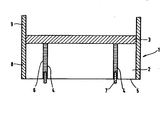
- FIG. 1 shows a sensor element according to the invention in cross section.
- the sensor element 1 has a substrate 2, on the front of which a sensor layer 3 is applied.
- the sensor layer 3 covers the entire cross section of the substrate 1.
- two signal lines 4 are arranged such that they the Back side of the sensor layer 3 facing the substrate 1 with the back side 5 of the substrate connect.
- the signal lines 4 lie in line-shaped, here cylindrical, Cavities 6 and consist of a metal with which the cavities 6 are filled are.
- Contact pins 7 are introduced into the cavities 6 from the back of the substrate 5 and firmly connected to the metal present in the cavities 6.
- the substrate 2 and the sensor layer 3 are surrounded by a protective device 8 which, preferably sealing against the substance, on the substrate side surfaces is trained.
- the protective device 8 stands above the surface of the Sensor layer 3 over.
- the length of the protruding part 9 of the protective device 8 The sensor layer 3 is selected depending on the substance to be measured. It is essential that it is prevented that the substance to be measured on the Back of the sensor element 1 arrives where the electrical contacts, here the Contact pin 7.
- the protruding part 9 of the protective device 8 can with a Connection device to be provided to the devices for feeding or discharging the measuring substance, such as pumps, valves, etc., can be connected.
- the sensor layer 3 is opened applied to the substrate 2 in a conventional manner.
- very small sensor elements In particular in semiconductor technology, it is often common to use multiple sensor elements 1 in to manufacture a body. According to conventional methods, if so is required, the back of the body is thinned and other appropriate Process steps carried out. Then the cavities 6 in the Sensor elements 1 formed and filled with a suitable metal.
- the Contact pins 7 are connected to the signal lines 4, for example by soldering, welding, Glue etc., attached. Then the sensor elements 1 are separated from each other.
- the protective device 8 can be, for example Heat shrink tubing, which by heat treatment on the side surfaces of the Substrate 2 is attached sealingly against the substance.
- the protective device 8 can also be generated, for example, by a press fit of a metal.
Landscapes
- Chemical & Material Sciences (AREA)
- Chemical Kinetics & Catalysis (AREA)
- Electrochemistry (AREA)
- Physics & Mathematics (AREA)
- Health & Medical Sciences (AREA)
- Life Sciences & Earth Sciences (AREA)
- Analytical Chemistry (AREA)
- Biochemistry (AREA)
- General Health & Medical Sciences (AREA)
- General Physics & Mathematics (AREA)
- Immunology (AREA)
- Pathology (AREA)
- Investigating Or Analyzing Materials By The Use Of Fluid Adsorption Or Reactions (AREA)
- Investigating Or Analyzing Materials By The Use Of Electric Means (AREA)
Claims (8)
- Elément capteur pour la mise en évidence de substances liquides, gazeuses ou fluides, comportant une couche de capteur (4) réalisée sur un substrat (7), dans lequel un circuit d'acheminement des signaux pour acheminer un signal de capteur est agencé dans le substrat (2) de telle sorte qu'il relie à la face postérieure de substrat (5) la face postérieure, tournée vers le substrat (2), de la couche de capteur (3), caractérisé en ce qu'est réalisé un dispositif de protection (8) limitant les surfaces latérales du substrat (2), faisant saillie au-delà de la couche de capteur et fournissant un étanchement vis-à-vis des substances à mettre en évidence.
- Elément capteur selon la revendication 1, caractérisé en ce que le circuit d'acheminement des signaux comprend des cavités (6) en forme de conduits (6) destinés à recevoir des lignes de signaux (4), lesquelles s'étendent depuis la face postérieure de la couche de capteur jusqu'à la face postérieure de substrat (5) ou jusqu'à la/les surface(s) latérales(s) de substrat.
- Elément capteur selon l'une ou l'autre des revendications 1 et 2, caractérisé en ce que les cavités (6) sont remplies d'un métal.
- Elément capteur selon l'une des revendications précédentes, caractérisé en ce que la couche de capteur (3) s'étend sensiblement sur toute la section transversale du substrat (2).
- Elément capteur selon l'une des revendications précédentes, caractérisé en ce que l'extrémité supérieure du dispositif de protection (8) est pourvue d'un dispositif de raccordement.
- Elément capteur selon l'une des revendications précédentes, caractérisé en ce que le substrat (2) est un substrat en semi-conducteur.
- Elément capteur selon l'une des revendications précédentes, caractérisé en ce que le substrat (2) est un substrat en verre.
- Procédé de fabrication d'un élément capteur pour la mise en évidence de substances liquides, gazeuses ou fluides, dans lequel une couche de capteur est réalisée sur un substrat, et un circuit d'acheminement des signaux pour acheminer un signal de capteur est réalisé dans le substrat de telle sorte que le circuit d'acheminement des signaux relie à la face postérieure de substrat ou aux surfaces latérales du substrat la face postérieure, tournée vers le substrat, de la couche de capteur, caractérisé en ce qu'est réalisé un dispositif de protection limitant les surfaces latérales du substrat, faisant saillie au-delà de la couche de capteur et fournissant un étanchement vis-à-vis des substances à mettre en évidence.
Applications Claiming Priority (2)
| Application Number | Priority Date | Filing Date | Title |
|---|---|---|---|
| DE19621227A DE19621227C2 (de) | 1996-05-25 | 1996-05-25 | Sensorelement zum Nachweis von flüssigen, gasförmigen oder fluiden Substanzen |
| DE19621227 | 1996-05-25 |
Publications (2)
| Publication Number | Publication Date |
|---|---|
| EP0809100A1 EP0809100A1 (fr) | 1997-11-26 |
| EP0809100B1 true EP0809100B1 (fr) | 2004-11-17 |
Family
ID=7795391
Family Applications (1)
| Application Number | Title | Priority Date | Filing Date |
|---|---|---|---|
| EP97107121A Expired - Lifetime EP0809100B1 (fr) | 1996-05-25 | 1997-04-29 | Capteur pour la détection des fluides et méthode de production |
Country Status (3)
| Country | Link |
|---|---|
| EP (1) | EP0809100B1 (fr) |
| JP (1) | JPH10132772A (fr) |
| DE (2) | DE19621227C2 (fr) |
Families Citing this family (3)
| Publication number | Priority date | Publication date | Assignee | Title |
|---|---|---|---|---|
| EP1189281B1 (fr) * | 1998-06-30 | 2007-08-22 | Micronas GmbH | Agencement de puce électronique |
| DE10156227C1 (de) * | 2001-11-15 | 2003-05-28 | Schott Glas | pH-Einstabmeßkette mit einem Diaphragma-Verschluß |
| DE102007036473A1 (de) * | 2007-08-01 | 2009-02-05 | Testo Ag | Vorrichtung zum Messen des Zustands eines Messguts, insbesondere von Ölen oder Fetten |
Citations (2)
| Publication number | Priority date | Publication date | Assignee | Title |
|---|---|---|---|---|
| JPH02269947A (ja) * | 1989-04-11 | 1990-11-05 | Matsushita Electric Ind Co Ltd | 燃焼制御用センサ |
| WO1996007094A1 (fr) * | 1994-08-30 | 1996-03-07 | Kavlico Corporation | Detecteur de deterioration d'huile |
Family Cites Families (7)
| Publication number | Priority date | Publication date | Assignee | Title |
|---|---|---|---|---|
| US4151503A (en) * | 1977-10-05 | 1979-04-24 | Ford Motor Company | Temperature compensated resistive exhaust gas sensor construction |
| DE4013593A1 (de) * | 1990-04-27 | 1991-10-31 | Biotechnolog Forschung Gmbh | Verfahren und sensor fuer amperometrische messprinzipien mit dickschicht-biosensoren |
| US5391272A (en) * | 1992-03-06 | 1995-02-21 | Andcare, Inc. | Electrochemical immunoassay methods |
| DE4230602C2 (de) * | 1992-09-12 | 1995-04-20 | Draegerwerk Ag | Elektrochemischer Sensor mit modularem Aufbau |
| US5284566A (en) * | 1993-01-04 | 1994-02-08 | Bacharach, Inc. | Electrochemical gas sensor with wraparound reference electrode |
| US5417100A (en) * | 1993-03-10 | 1995-05-23 | Hughes Aircraft Company | Reversible sensor for detecting solvent vapors |
| US5511428A (en) * | 1994-06-10 | 1996-04-30 | Massachusetts Institute Of Technology | Backside contact of sensor microstructures |
-
1996
- 1996-05-25 DE DE19621227A patent/DE19621227C2/de not_active Expired - Fee Related
-
1997
- 1997-04-29 EP EP97107121A patent/EP0809100B1/fr not_active Expired - Lifetime
- 1997-04-29 DE DE59712078T patent/DE59712078D1/de not_active Expired - Fee Related
- 1997-05-26 JP JP9135625A patent/JPH10132772A/ja active Pending
Patent Citations (2)
| Publication number | Priority date | Publication date | Assignee | Title |
|---|---|---|---|---|
| JPH02269947A (ja) * | 1989-04-11 | 1990-11-05 | Matsushita Electric Ind Co Ltd | 燃焼制御用センサ |
| WO1996007094A1 (fr) * | 1994-08-30 | 1996-03-07 | Kavlico Corporation | Detecteur de deterioration d'huile |
Also Published As
| Publication number | Publication date |
|---|---|
| JPH10132772A (ja) | 1998-05-22 |
| DE19621227C2 (de) | 2003-02-20 |
| DE59712078D1 (de) | 2004-12-23 |
| EP0809100A1 (fr) | 1997-11-26 |
| DE19621227A1 (de) | 1997-11-27 |
Similar Documents
| Publication | Publication Date | Title |
|---|---|---|
| EP1518098B1 (fr) | Capteur haute pression comprenant une membrane de silicium et une couche de brasure | |
| WO2005047878A1 (fr) | Ensemble de detection comportant plusieurs capteurs potentiometriques | |
| DE69936199T2 (de) | Sensorpackung mit einer integrierten pfropfenelektrode | |
| EP1396718B1 (fr) | Capteur électrochimique | |
| EP1917509A1 (fr) | Dispositif de detection comportant un substrat et un boitier et procede de fabrication d'un dispositif de detection | |
| DE10325020A1 (de) | Verfahren zum Versiegeln eines Halbleiterbauelements und eine Vorrichtung, die das Verfahren ausführt | |
| DE69734039T2 (de) | Vorrichtung mit zwei mikromechanischen Substraten für ein mikromechanisches System oder Teil eines mikromechanischen Systems und Verfahren zur Zusammensetzung zweier mikromechanischer Substrate | |
| EP2435797A2 (fr) | Élément capteur | |
| EP1740932B1 (fr) | Cellule de mesure, son procédé de production | |
| DE19611964A1 (de) | Gasmeßfühler | |
| DE2736200A1 (de) | Chemisch sensitiver feldeffekt- transistor und verfahren zur herstellung desselben | |
| DE102009018364A1 (de) | Vorrichtung zur Detektion eines Gases oder Gasgemisches und Verfahren zum Herstellen einer solchen | |
| DE102004045896A1 (de) | Transponder mit Antenne und Flip-Chip-Modul und Verfahren zu dessen Herstellung | |
| DE102018108744A1 (de) | Verfahren zur Herstellung eines Drucksensors | |
| DE69218004T2 (de) | Flussmittelloses lötverfahren | |
| DE102005027365A1 (de) | Hochdrucksensoreinrichtung und Verfahren zu ihrer Herstellung | |
| DE202009013919U1 (de) | Drucktransmitter | |
| DE19621227C2 (de) | Sensorelement zum Nachweis von flüssigen, gasförmigen oder fluiden Substanzen | |
| DE19843471B4 (de) | Druckerkennungsvorrichtung | |
| DE102005012355B4 (de) | Kompakter Drucksensor mit hoher Korrosionsbeständigkeit und hoher Genauigkeit | |
| EP1204301B1 (fr) | Agencement pour constituer un circuit d'entrée pour l'enregistrement et le traitement d'un signal électrique | |
| DE102012111811A1 (de) | Elektrochemischer Sensor zur Erfassung einer Analytkonzentration in einem Messmedium | |
| WO2008098954A1 (fr) | Appareil de mesure modulaire | |
| EP1475623B1 (fr) | Dispositif de mesure de pression avec connection transversale et procédé de connection | |
| DE19845537A1 (de) | Sensor und Verfahren zu seiner Herstellung |
Legal Events
| Date | Code | Title | Description |
|---|---|---|---|
| PUAI | Public reference made under article 153(3) epc to a published international application that has entered the european phase |
Free format text: ORIGINAL CODE: 0009012 |
|
| AK | Designated contracting states |
Kind code of ref document: A1 Designated state(s): DE FR GB IT NL |
|
| RAP1 | Party data changed (applicant data changed or rights of an application transferred) |
Owner name: MICRONAS SEMICONDUCTOR HOLDING AG |
|
| 17P | Request for examination filed |
Effective date: 19980526 |
|
| RAP1 | Party data changed (applicant data changed or rights of an application transferred) |
Owner name: MICRONAS SEMICONDUCTOR HOLDING AG |
|
| 17Q | First examination report despatched |
Effective date: 20030611 |
|
| GRAP | Despatch of communication of intention to grant a patent |
Free format text: ORIGINAL CODE: EPIDOSNIGR1 |
|
| GRAS | Grant fee paid |
Free format text: ORIGINAL CODE: EPIDOSNIGR3 |
|
| GRAA | (expected) grant |
Free format text: ORIGINAL CODE: 0009210 |
|
| AK | Designated contracting states |
Kind code of ref document: B1 Designated state(s): DE FR GB IT NL |
|
| REG | Reference to a national code |
Ref country code: GB Ref legal event code: FG4D Free format text: NOT ENGLISH |
|
| GBT | Gb: translation of ep patent filed (gb section 77(6)(a)/1977) |
Effective date: 20041117 |
|
| REF | Corresponds to: |
Ref document number: 59712078 Country of ref document: DE Date of ref document: 20041223 Kind code of ref document: P |
|
| ET | Fr: translation filed | ||
| PLBE | No opposition filed within time limit |
Free format text: ORIGINAL CODE: 0009261 |
|
| STAA | Information on the status of an ep patent application or granted ep patent |
Free format text: STATUS: NO OPPOSITION FILED WITHIN TIME LIMIT |
|
| 26N | No opposition filed |
Effective date: 20050818 |
|
| PGFP | Annual fee paid to national office [announced via postgrant information from national office to epo] |
Ref country code: NL Payment date: 20070424 Year of fee payment: 11 |
|
| PGFP | Annual fee paid to national office [announced via postgrant information from national office to epo] |
Ref country code: GB Payment date: 20070425 Year of fee payment: 11 |
|
| PGFP | Annual fee paid to national office [announced via postgrant information from national office to epo] |
Ref country code: IT Payment date: 20070521 Year of fee payment: 11 |
|
| PGFP | Annual fee paid to national office [announced via postgrant information from national office to epo] |
Ref country code: FR Payment date: 20070417 Year of fee payment: 11 |
|
| PGFP | Annual fee paid to national office [announced via postgrant information from national office to epo] |
Ref country code: DE Payment date: 20080602 Year of fee payment: 12 |
|
| GBPC | Gb: european patent ceased through non-payment of renewal fee |
Effective date: 20080429 |
|
| NLV4 | Nl: lapsed or anulled due to non-payment of the annual fee |
Effective date: 20081101 |
|
| PG25 | Lapsed in a contracting state [announced via postgrant information from national office to epo] |
Ref country code: NL Free format text: LAPSE BECAUSE OF NON-PAYMENT OF DUE FEES Effective date: 20081101 |
|
| REG | Reference to a national code |
Ref country code: FR Ref legal event code: ST Effective date: 20081231 |
|
| PG25 | Lapsed in a contracting state [announced via postgrant information from national office to epo] |
Ref country code: FR Free format text: LAPSE BECAUSE OF NON-PAYMENT OF DUE FEES Effective date: 20080430 |
|
| PG25 | Lapsed in a contracting state [announced via postgrant information from national office to epo] |
Ref country code: GB Free format text: LAPSE BECAUSE OF NON-PAYMENT OF DUE FEES Effective date: 20080429 |
|
| PG25 | Lapsed in a contracting state [announced via postgrant information from national office to epo] |
Ref country code: IT Free format text: LAPSE BECAUSE OF NON-PAYMENT OF DUE FEES Effective date: 20080429 |
|
| PG25 | Lapsed in a contracting state [announced via postgrant information from national office to epo] |
Ref country code: DE Free format text: LAPSE BECAUSE OF NON-PAYMENT OF DUE FEES Effective date: 20091103 |