EP0810493A2 - Appareil de formation d'images - Google Patents
Appareil de formation d'images Download PDFInfo
- Publication number
- EP0810493A2 EP0810493A2 EP97303614A EP97303614A EP0810493A2 EP 0810493 A2 EP0810493 A2 EP 0810493A2 EP 97303614 A EP97303614 A EP 97303614A EP 97303614 A EP97303614 A EP 97303614A EP 0810493 A2 EP0810493 A2 EP 0810493A2
- Authority
- EP
- European Patent Office
- Prior art keywords
- toner
- developer
- supporting medium
- image forming
- control electrode
- Prior art date
- Legal status (The legal status is an assumption and is not a legal conclusion. Google has not performed a legal analysis and makes no representation as to the accuracy of the status listed.)
- Granted
Links
- 230000002401 inhibitory effect Effects 0.000 claims abstract description 4
- 230000001276 controlling effect Effects 0.000 claims description 23
- 239000002245 particle Substances 0.000 claims description 9
- 230000000007 visual effect Effects 0.000 claims description 5
- 239000000463 material Substances 0.000 claims description 2
- 230000002093 peripheral effect Effects 0.000 abstract description 53
- 238000009413 insulation Methods 0.000 description 5
- 230000015556 catabolic process Effects 0.000 description 4
- 230000007547 defect Effects 0.000 description 4
- 238000006731 degradation reaction Methods 0.000 description 4
- 230000009191 jumping Effects 0.000 description 4
- 239000011800 void material Substances 0.000 description 4
- 230000005684 electric field Effects 0.000 description 3
- XAGFODPZIPBFFR-UHFFFAOYSA-N aluminium Chemical compound [Al] XAGFODPZIPBFFR-UHFFFAOYSA-N 0.000 description 2
- 229910052782 aluminium Inorganic materials 0.000 description 2
- 239000003086 colorant Substances 0.000 description 2
- 230000007812 deficiency Effects 0.000 description 2
- 230000000593 degrading effect Effects 0.000 description 2
- 238000010438 heat treatment Methods 0.000 description 2
- RYGMFSIKBFXOCR-UHFFFAOYSA-N Copper Chemical compound [Cu] RYGMFSIKBFXOCR-UHFFFAOYSA-N 0.000 description 1
- 239000002033 PVDF binder Substances 0.000 description 1
- 239000011889 copper foil Substances 0.000 description 1
- 230000007423 decrease Effects 0.000 description 1
- 229910052736 halogen Inorganic materials 0.000 description 1
- 150000002367 halogens Chemical class 0.000 description 1
- 238000005259 measurement Methods 0.000 description 1
- 238000002844 melting Methods 0.000 description 1
- 230000008018 melting Effects 0.000 description 1
- 238000000034 method Methods 0.000 description 1
- 108091008695 photoreceptors Proteins 0.000 description 1
- 229920001721 polyimide Polymers 0.000 description 1
- 239000009719 polyimide resin Substances 0.000 description 1
- 229920002981 polyvinylidene fluoride Polymers 0.000 description 1
- 230000001105 regulatory effect Effects 0.000 description 1
- 229920002050 silicone resin Polymers 0.000 description 1
- 230000003068 static effect Effects 0.000 description 1
- 239000000758 substrate Substances 0.000 description 1
- 230000001360 synchronised effect Effects 0.000 description 1
- 238000011144 upstream manufacturing Methods 0.000 description 1
Images




Classifications
-
- B—PERFORMING OPERATIONS; TRANSPORTING
- B41—PRINTING; LINING MACHINES; TYPEWRITERS; STAMPS
- B41J—TYPEWRITERS; SELECTIVE PRINTING MECHANISMS, i.e. MECHANISMS PRINTING OTHERWISE THAN FROM A FORME; CORRECTION OF TYPOGRAPHICAL ERRORS
- B41J2/00—Typewriters or selective printing mechanisms characterised by the printing or marking process for which they are designed
- B41J2/385—Typewriters or selective printing mechanisms characterised by the printing or marking process for which they are designed characterised by selective supply of electric current or selective application of magnetism to a printing or impression-transfer material
- B41J2/41—Typewriters or selective printing mechanisms characterised by the printing or marking process for which they are designed characterised by selective supply of electric current or selective application of magnetism to a printing or impression-transfer material for electrostatic printing
- B41J2/415—Typewriters or selective printing mechanisms characterised by the printing or marking process for which they are designed characterised by selective supply of electric current or selective application of magnetism to a printing or impression-transfer material for electrostatic printing by passing charged particles through a hole or a slit
- B41J2/4155—Typewriters or selective printing mechanisms characterised by the printing or marking process for which they are designed characterised by selective supply of electric current or selective application of magnetism to a printing or impression-transfer material for electrostatic printing by passing charged particles through a hole or a slit for direct electrostatic printing [DEP]
-
- G—PHYSICS
- G03—PHOTOGRAPHY; CINEMATOGRAPHY; ANALOGOUS TECHNIQUES USING WAVES OTHER THAN OPTICAL WAVES; ELECTROGRAPHY; HOLOGRAPHY
- G03G—ELECTROGRAPHY; ELECTROPHOTOGRAPHY; MAGNETOGRAPHY
- G03G15/00—Apparatus for electrographic processes using a charge pattern
- G03G15/22—Apparatus for electrographic processes using a charge pattern involving the combination of more than one step according to groups G03G13/02 - G03G13/20
- G03G15/34—Apparatus for electrographic processes using a charge pattern involving the combination of more than one step according to groups G03G13/02 - G03G13/20 in which the powder image is formed directly on the recording material, e.g. by using a liquid toner
- G03G15/344—Apparatus for electrographic processes using a charge pattern involving the combination of more than one step according to groups G03G13/02 - G03G13/20 in which the powder image is formed directly on the recording material, e.g. by using a liquid toner by selectively transferring the powder to the recording medium, e.g. by using a LED array
- G03G15/346—Apparatus for electrographic processes using a charge pattern involving the combination of more than one step according to groups G03G13/02 - G03G13/20 in which the powder image is formed directly on the recording material, e.g. by using a liquid toner by selectively transferring the powder to the recording medium, e.g. by using a LED array by modulating the powder through holes or a slit
Definitions
- the present invention relates to an image forming apparatus such as a digital copier, facsimile machine, laser printer and the like, in particular relating to an image forming apparatus which forms images by causing developer particles to jump to the recording medium.
- the image forming apparatus includes an image forming unit 51 having a toner supplying section 52 and a printing section 53.
- toner 71 is made to jump from toner supplying section 52 and adhere to a sheet of paper 55, the recording medium. During this, the jumping of toner 71 is controlled in accordance with the image data.
- Toner supplying section 52 is composed of a toner reservoir 70 for holding toner 71 as developer particles which are negatively charged, and a toner support 72 which supports toner 71 on its peripheral surface by magnetic force whilst rotating in the direction of arrow E.
- Printing section 53 is composed of an opposing electrode 75 of a cylindrical shape and a control electrode 76 which is provided between opposing electrode 75 and toner support 72. Opposing electrode 75 rotates in the direction of arrow F so that paper 55 is conveyed between opposing electrode 75 and control electrode 76 in the direction of arrow G.
- control electrode 76 has a plurality of gates 79 formed therein, each gate 79 having an annular electrode 77 formed around the edge thereof.
- each gate 79 having an annular electrode 77 formed around the edge thereof.
- toner 71 supported on the peripheral surface of toner support 72 is made to jump toward opposing electrode 75 and pass through selective gates 79 hence being made to adhere to paper 55 which is placed between opposing electrode 75 and control electrode 76.
- the image forming apparatus configured as above is one which directly forms the image on the surface of recording medium such as paper etc. Therefore, it is no longer necessary to use a developer medium such as a photoreceptor etc., which was used in conventional image forming apparatuses. Further, the operation for transferring the image from the developer medium to the paper can be omitted, thus making it possible to eliminate degradation of the image due to the existence of this operation. Moreover, the structure of the apparatus can be simplified needing fewer parts, thus making it possible to reduce the apparatus in size and cost.
- toner support 72 might partially lack the toner 71, which may be needed for later transfer. Therefore, the amount of toner 71 transferred through gate 79n+1 becomes low resulting in insufficient dot density and dot diameter in the formed image, lowering the image contrast and degrading the reproduction of halftone. In color image forming apparatus, it becomes impossible to reproduce the desired colors. Moreover, image deficiency such as white strips and color voids may occur.
- toner 71 on the peripheral surface of toner support 72 needs to be increased.
- toner density on toner support 72 there is a limit for the toner density on toner support 72, and it is impossible to obtain an adequate toner density under the present conditions.
- the thickness of the toner layer on toner support 72 tends to become unstable and in some cases, it may become difficult to obtain the desired layer thickness, making it impossible to form an stable image.
- control electrode 76 when the thickness of the toner layer on toner support 72 is enhanced to increase the density of toner 71, the distance between control electrode 76 and toner 71 becomes shortened. This means that toner 71 becomes more likely to adhere to control electrode 76 and becomes further unstable in its layer thickness. If toner 71 has adhered to control electrode 76, the potential created by the charge carried by toner 71 changes the potential of control electrode 76 resulting in an ineptness in controlling the potential used for image forming. This also causes obstruction or clogging in gates 79.
- control electrode 76 In order to avoid the above situation, if control electrode 76 is made more distant from toner support 72, the potentials to be applied to toner support 72, opposing electrode 75 and control electrode 76 need to be increased, resulting in increase in cost for the power source. In addition, the elevation of the potential applied to opposing electrode 75 requires a more thorough insulation and also the price for the high-voltage driver for switching the potential applied to control electrode 76 increases.
- the present invention has been devised to attain the above object, and the gist of the invention is as follows:
- an image forming apparatus comprises: a supporting medium for supporting the developer; an opposing electrode spaced a predetermined distance apart from the supporting medium and disposed facing the supporting medium; a control electrode disposed between the supporting medium and the opposing electrode and having a plurality of gates which form passage for the developer particles; and a drive controlling means which moves the surface of the supporting medium at a constant velocity relative to the control electrode, so that the image forming apparatus forms a visual image on a recording medium conveyed between the opposing electrode and the control electrode whilst varying the potential applied to the control electrode so as to selectively control transfer of the developer particles through the gates, and is constructed such that the moving velocity of the supporting medium surface controlled by the drive controlling means is set at a higher rate than the moving velocity of the recording medium relative to control electrode.
- an image forming apparatus having the above first feature is constructed such that the moving velocity of the supporting medium surface controlled by the drive controlling means is set up based on the moving velocity of recording medium relative to the control electrode, conditions of the arrangement of the gates in the control electrode and the size of the area where no developer adhere to, which is produced on supporting medium surface by the transfer of the developer through the gate.
- an image forming apparatus having the above second feature is constructed such the moving velocity vs of the supporting medium surface controlled by the drive controlling means is set up so as to satisfy the following condition: vs ⁇ (d/t) ⁇ cos ⁇ - (1/t) (L 2 - d 2 sin 2 ⁇ ) 1/2
- t is the shortest time interval between the voltage application to one gate and the voltage application to the proximal gate
- d is the distance between the centers of the two gates for which the times of voltage application is closest to each other
- L is the maximum length of developer-free area on the supporting medium surface
- ⁇ is the angle of the slant connected between the centers of the two gates for which the times of voltage application is closet to each other, with respect to the conveying direction of the recording medium.
- an image forming apparatus having the above second or third feature is constructed such that the moving velocity vs of the supporting medium surface controlled by the drive controlling means is set up so as to satisfy the following condition: L ⁇ vs ⁇ T where L is the maximum length of developer-free area on the supporting medium surface and T is the shortest period of time during which the voltage for inhibiting passage of the developer is applied to an identical gate.
- Fig.3 is a view showing the configuration of an image forming apparatus of a typical embodiment of the invention.
- This image forming apparatus has an image forming unit 1 which is composed of a toner supplying section 2 and a printing section 3.
- Image forming unit 1 creates a visual image in accordance with an image signal, onto a sheet of paper as recording medium with toner as the developer.
- the toner is made to jump and adhere onto the paper whilst the jumping of the toner is controlled based on the image forming signal, so as to directly form the image on the paper.
- a paper feeder 10 which is composed of a paper cassette 4 for storing sheets of paper 5 as recording medium, a pickup roller 6 for delivering paper 5 supplied from paper cassette 4, and a paper guide 7 for guiding paper 5 sent out.
- Pickup roller 6 receives rotational force from an unillustrated driver.
- Fixing unit 11 for heating and pressurizing the toner image which was formed on paper 5 at the image forming unit 1, to fix it onto paper 5.
- Fixing unit 11 is composed of a heat roller 12, a heater 13, a pressure roller 14, a temperature sensor 15, and an unillustrated temperature controller circuit.
- Heat roller 12 is made up of, for example, an aluminum pipe of about 2 mm thick.
- Heater 13 is a halogen lamp, for example, which is incorporated in heat roller 12.
- Pressure roller 14 is a pipe made up of silicone resin, for example. Heat roller 12 and pressure roller 14 are pressed against one another with a constant pressure.
- Temperature sensor 15 measures the surface temperature of heat roller 12.
- Temperature controlling circuit controls the operation of heater 13 based on the measurement result from temperature sensor 15 so that the surface temperature of heat roller 12 is maintained at 150°C, for example, which allows the melting of the toner.
- Fixing unit 11 has an unillustrated paper discharge sensor for detecting the discharge of paper 5.
- fixing unit 11 may be constructed so that the toner image is fixed by heating or pressing paper 5.
- Toner supplying section 2 in image forming apparatus 1 is composed of a toner reservoir 20 for storing toner 21 as the developer, a cylindrical support 22 for magnetically supporting toner 21, a doctor blade 23 which imparts charge to toner 21 and regulates the thickness of the toner layer carried on the peripheral surface of toner support 22.
- Doctor blade 23 is arranged on the upstream side of toner support 22 with respect to the rotational direction of the peripheral surface of toner support 22, spaced with a distance of about 60 ⁇ m, for example, from the peripheral surface of toner support 22.
- Toner 21 is of a magnetic type having a mean particle diameter of, for example, 6 ⁇ m, and is electrified with static charge of -4 ⁇ C/g to -5 ⁇ C/g by doctor blade 23.
- Toner support 22 receives rotational force from driver controller 33 so that it rotates at a constant peripheral speed in the direction indicated by arrow A. Toner support 22 is grounded and has unillustrated fixed magnets therein, at the position opposite doctor blade 23 and at the position opposite a control electrode 26 (which will be described later). This arrangement permits toner support 22 to magnetically carry toner 21 on its peripheral surface, and toner 21 supported on the peripheral surface of toner support 22 is made to stand up in 'spikes' at the areas corresponding to the positions of the magnets. Toner support 22 can be configured so as to support toner 21 by electric force or combination of electric and magnetic forces.
- Printing section 3 includes: a dielectric belt 24 tensioned between a pair of support rollers 16a and 16b at the position opposite the peripheral surface of toner support 22; an opposing electrode 25 which is in contact with the inner peripheral surface of the upper side of dielectric belt 24; a high-voltage power source 30 for applying a high voltage to opposing electrode 25; a control electrode 26 provided between toner support 22 and opposing electrode 25; a charge eraser brush 32 which is in contact with the outer peripheral surface of dielectric belt 24; a charge eraser power source 17 for imparting a charge eraser voltage to charge eraser brush 32; a cleaner 19 abutting the outer peripheral surface of dielectric belt 24; and a charging brush 8 for electrifying paper 5 whilst it is being conveyed along the upper surface of dielectric belt 24.
- Opposing electrode 25 is made up of an aluminum plate of, for example, about 1 mm thick, and is arranged about 1 mm apart from the peripheral surface of toner support 22.
- Dielectric belt 24 is made of, for example, PVDF as a base material of about 75 ⁇ m thick with a volume resistivity of about 10 10 ⁇ cm.
- Support rollers 16a and 16b supporting dielectric belt 24 is rotated by an unillustrated driver in the direction of arrow B at a constant peripheral velocity.
- Applied to opposing electrode 25 is a high voltage, e.g., 2.3 kV from high voltage power source 30. This arrangement generates an electric field between opposing electrode 25 and toner support 22, required for causing toner 21 being supported on the peripheral surface of toner support 22 to jump toward opposing electrode 25.
- Charge eraser brush 32 is pressed against dielectric belt 24 on the control electrode 26 side, relative to the rotational direction of dielectric belt 24.
- Charge eraser brush 32 has an eraser potential of, for example, about 2.5 kV applied from charge eraser power source 17 so as to eliminate unnecessary charges on the surface of dielectric belt 24.
- Cleaner 19 removes the toner adhering to the outer peripheral surface of dielectric belt 24. For example, if paper jam or some other defects occur, the toner adhering to the outer peripheral surface of dielectric belt 24 stains the underside of the next conveyed paper 5. The cleaner prevents this.
- this image forming apparatus includes: a main controller as a control circuit for controlling the whole image forming apparatus; an image processor for converting the image data which was obtained from image pickup device into an image data format by which the image can be printed; an image memory for storing the converted image data; and an image forming control unit for converting the image data obtained from the image processor into the image data to be given to control electrode 26.
- Fig.4 is a plan view showing the control electrode provided in the above image forming apparatus.
- Control electrode 26 is supported parallel to opposing electrode 25 by means of an unillustrated supporter member so that its distance from the peripheral surface of toner support 22 is set at, for example, 100 ⁇ m.
- Control electrode 26 is composed of an insulative plate-like member made of a polyimide resin or the like of about 75 ⁇ m thick with a plurality of annular electrodes 27 formed independently of each other. Annular electrodes 27 are individually formed around the edges of respective plural holes or gates 29. Annular electrodes 27 are formed of copper foil, for example, of 30 ⁇ m.
- Each gate 29 forms a passage for toner 21 to jump from the peripheral surface of toner support 22 toward opposing electrode 25.
- Each annular electrode 27 is connected to a control power source 31 via a respective feeder line 28 and an unillustrated high voltage driver.
- gates 29 as well as annular electrodes 27 are formed at 2,560 sites, for instance. This number corresponds to a resolution of 300 DPI across the width of A4 sized paper, or in the direction perpendicular to the conveyance direction of the paper.
- the surface of annular electrodes 27 as well as the surface of feeder lines 28 is coated with an insulative layer of 30 ⁇ m thick, thus ensuring insulation between annular electrodes 27, insulation between feeder lines 28, and insulation between annular electrodes 27 and feeder lines 28, not related to each other.
- control electrode 26 By controlling the potential to be applied to annular electrodes 27 of control electrode 26, the intensity of the electric field created between toner support 22 and opposing electrode 25 is changed so that the jumping of toner 21 from toner support 22 to opposing electrode 25 is controlled. Specifically, selective voltages are applied to annular electrode 27 from control power source 31 in accordance with the image data. When toner 21 supported on toner support 22 needs to be transferred toward opposing electrode 25, control power source 31 applies a voltage, e.g., 150 V to annular electrodes 27, whereas it applies another voltage, e.g., -200 V when the toner is not to be transferred.
- control power source 31 is controlled by a control-electrode controlling signal transmitted, from an unillustrated image forming control unit.
- Fig.5 is a flowchart showing the procedural flow of the image forming operation of the image forming apparatus.
- the image reading operation is effected.
- the image pickup section reads the original image, and the image data thus picked up is image processed in the image processing section to be stored into the image memory (s1-s3).
- This image data is transferred to the image forming control unit at a predetermined timing (s4) so that the image forming control unit transforms the input image data into a control-electrode controlling signal to be imparted to control electrode 26 (s5).
- the image forming control unit When the image forming control unit has created a predetermined amount of the control signal, it causes toner support 22 to rotate (s6, s7) while a voltage of -200 V is applied to control electrode 26 (s8). At the same time, the same voltage as applied to opposing electrode 25 also is applied to roller 16a from high voltage power source 30 (s8).
- Charging brush 8 is applied with a charging potential of 1.2 kV from charger power source 18 while charge eraser brush 32 is applied with an erasing potential from charge eraser power source 17 (s9).
- an unillustrated driver is activated to start rotating pickup roller 6 (s10).
- This rotation of pickup roller 6 delivers a sheet of paper out from paper cassette 4 toward image forming unit 1.
- paper 5 is conveyed between charging brush 8 and dielectric belt 24.
- Paper 5 is supplied with charge due to the potential difference between charging brush 8 and dielectric belt 24.
- Electrostatically attracted to dielectric belt 24 paper 5 is conveyed with the rotational movement of dielectric belt 24, to a position in printing section 3, where it faces toner support 22.
- control power source 31 supplies the control-electrode controlling signal to control power source 31 so that control power source 31 applies a high voltage to annular electrodes 27 of control electrode 26 (s12).
- This control-electrode controlling signal is supplied at a time synchronized with the conveyance of paper 5 by dielectric belt 24.
- Control power source 31 controls the high voltage to be applied to annular electrodes 27 based on the control-electrode controlling signal.
- a voltage, 150 V or -200 V is applied to each of designated annular electrodes 27 from control power source 31 so as to control the electric field near control electrode 26.
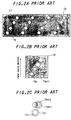
- Figs.6A and 6B are enlarged views showing essential components of the control electrode.
- voltage is first applied to annular electrode 27n of gate 29n and then applied to annular electrode 27n+1 of gate 29n+1.
- the voltage application to annular electrode 27n causes toner 21 to jump from the portion facing gate 29n on the peripheral surface of toner support 22 toward opposing electrode 25 thus forming a toner-free area 22n where no toner 21 exists as shown in Fig.6B.
- a plurality of gates 29 formed on control electrode 26 as a whole correspond to one line at right angle to the conveyance direction of the image. Therefore, if the movement of toner-free area 22n due to the rotation of toner support 22 during the time interval between voltage application to annular electrode 27n and to annular electrode 27n+1 is equal to the distance between gates 29n and 29n+1, part of area on toner support 22 facing gate 29n+1 overlaps toner-free area 22n as shown in Fig.6B when voltage application is performed to annular electrode 27n+1. For this reason, when voltage application is performed to annular electrode 27n+1, the amount of toner 21 transferred from the peripheral surface of toner support 22 decreases, causing a partial void in the image formed on paper 5.
- toner 21 on the peripheral surface of toner support 22 needs to be increased.
- toner density on toner support 22 there is a limit for the toner density on toner support 22, and it is impossible to obtain an adequate toner density under the present conditions.
- the thickness of the layer of toner 21 tends to become unstable and in some cases, it may become difficult to obtain the desired layer thickness, making it impossible to form an stable image.
- the distance between control electrode 26 and the layer of toner 21 becomes shortened. This means that toner 21 becomes more likely to adhere to control electrode 26 and becomes even further unstable in its layer thickness. If toner 21 has adhered to control electrode 26, the potential created by the charge carried by toner 21 changes the potential of control electrode 26 resulting in an ineptness in controlling the potential used for image forming. This also causes obstruction or clogging in gates 29. In order to avoid the above situation, if control electrode 26 is made more distant from toner support 22, the potentials to be applied to toner support 22, opposing electrode 25 and control electrode 26 need to be increased, resulting in increase in cost for the power source. In addition, the elevation of the potential applied to opposing electrode 25 requires a more thorough insulation and also the price for the high-voltage driver for switching the potential applied to control electrode 26 increases.
- toner-free area 22n produced on the peripheral surface of toner support 22 by the previous transfer through gate 29n overlaps the subsequent printing area designated at 22n+1 on the peripheral surface of toner support 22 that opposes gate 29n+1, thus area 22n+1 on the peripheral surface of toner support 22 partially lacks toner 21. Therefore, the amount of toner 21 supplied becomes low resulting in insufficient dot density and dot diameter in the formed image, lowering the image contrast and degrading the reproduction of halftone. In color image forming apparatus, it becomes impossible to reproduce the desired colors. Moreover, image deficiency such as white strips and color voids may occur.
- the above problem can be solved by specifying the peripheral velocity of toner support 22 based on the diameter and positional relationship of gates 29. More detailedly, the peripheral velocity of toner support 22 is regulated so that toner-free area 22n on the peripheral surface of toner support 22 which has been produced by the transfer of toner 21 through gate 29n, moves to a position where it will not overlap toner-free area 22n+1 facing gate 29n+1 when annular electrode 27n+1 provided in gate 29n+1 adjoining gate 29n is voltage applied.
- the peripheral velocity vs of toner support 22 must satisfy the following condition (1): vs ⁇ t ⁇ (d/t) ⁇ cos ⁇ - (1/t) (L 2 - d 2 sin 2 ⁇ ) 1/2 In this way, it is possible to set the peripheral velocity vs of toner support 22 at a rate higher than the conveyance speed of paper 5.
- the currently forming toner-free area 22n on the peripheral surface of toner support 22 needs to be adapted so as not to overlap the toner-free area 22n' formed at the time of the previous application of voltage to annular electrode gate 29n.
- the previous toner-free area 22n' must at least move up to the position shown in Fig.7B, or the position where it does not overlap the toner-free area 22n to be formed at the current event.
- the peripheral velocity vs of toner support 22 should fall within the following range: L/T ⁇ vs ⁇ (d/t) ⁇ cos ⁇ - (1/t) (L 2 - d 2 sin 2 ⁇ ) 1/2
- the peripheral velocity vs of toner support 22 should be above about 81 mm/sec and below about 438 mm/sec.
- the peripheral velocity vs of toner support 22 must satisfy the following condition: vs ⁇ (d/t) ⁇ cos ⁇ + (1/t) (L 2 - d 2 sin 2 ⁇ ) 1/2 .
- the peripheral velocity vs will take such a large value as vs ⁇ 1803 mm/sec. Therefore, the peripheral velocity of toner support 22 should and can be limited within a realistic range by imposing the condition, i.e., L ⁇ d.
- toner was used as the developer, it is also possible to use ink.
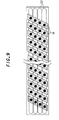
- control electrode 26 having annular electrodes 27 it is also possible to control toner transfer from the toner support by providing a plurality of strip-like electrodes 51 and 52 matrix-wise on both sides of the substrate as shown in Fig.9 and governing the voltage to be applied to the strip-like electrodes crossing over each other at right angles or at an angle.
- the present invention can be applied in the same manner to a color image forming apparatus, as shown in Fig.10, which has a plurality of image forming units 1a-1d made up of toner supplying sections 2a-2d and control electrodes 26a-26d wherein toner supplying sections 2a-2d are filled with toners, e.g., yellow, magenta, cyan and black.
- a color image forming apparatus as shown in Fig.10, which has a plurality of image forming units 1a-1d made up of toner supplying sections 2a-2d and control electrodes 26a-26d wherein toner supplying sections 2a-2d are filled with toners, e.g., yellow, magenta, cyan and black.
- the present invention can be also applied in the same manner to a configuration which uses an ion flow process in its toner supplying section.
- the developer when the developer has been made to jump through an arbitrary gate of the control electrode and subsequently the developer is made to jump through its adjoining gate, it is possible to prevent the amount of the developer at the second transfer from being affected by the developer free-area which has been produced on the peripheral support of the toner support by the first developer transfer, and therefore it is possible to secure an adequate amount of developer even when the developer is made to jump through a plurality of adjoining gates. Accordingly, degradation of image forming states such as image defects or void etc., due to an insufficient amount of developer can be definitely prevented.
Landscapes
- Physics & Mathematics (AREA)
- General Physics & Mathematics (AREA)
- Printers Or Recording Devices Using Electromagnetic And Radiation Means (AREA)
- Electrophotography Using Other Than Carlson'S Method (AREA)
Applications Claiming Priority (3)
| Application Number | Priority Date | Filing Date | Title |
|---|---|---|---|
| JP8133279A JPH09314889A (ja) | 1996-05-28 | 1996-05-28 | 画像形成装置 |
| JP133279/96 | 1996-05-28 | ||
| JP13327996 | 1996-05-28 |
Publications (3)
| Publication Number | Publication Date |
|---|---|
| EP0810493A2 true EP0810493A2 (fr) | 1997-12-03 |
| EP0810493A3 EP0810493A3 (fr) | 1997-12-17 |
| EP0810493B1 EP0810493B1 (fr) | 2002-10-16 |
Family
ID=15100929
Family Applications (1)
| Application Number | Title | Priority Date | Filing Date |
|---|---|---|---|
| EP97303614A Expired - Lifetime EP0810493B1 (fr) | 1996-05-28 | 1997-05-28 | Appareil de formation d'images |
Country Status (5)
| Country | Link |
|---|---|
| US (1) | US6056390A (fr) |
| EP (1) | EP0810493B1 (fr) |
| JP (1) | JPH09314889A (fr) |
| CN (1) | CN1106597C (fr) |
| DE (1) | DE69716340T2 (fr) |
Families Citing this family (3)
| Publication number | Priority date | Publication date | Assignee | Title |
|---|---|---|---|---|
| JP4156359B2 (ja) * | 2002-12-20 | 2008-09-24 | シャープ株式会社 | 現像装置 |
| JP5206026B2 (ja) * | 2007-03-16 | 2013-06-12 | 株式会社リコー | 画像形成装置、プロセスカートリッジ及び画像形成方法 |
| JP4771484B2 (ja) * | 2007-05-07 | 2011-09-14 | 有限会社 福岡テクノ研工業 | 画像形成方法及び画像形成装置 |
Family Cites Families (9)
| Publication number | Priority date | Publication date | Assignee | Title |
|---|---|---|---|---|
| JPH04239661A (ja) * | 1991-01-24 | 1992-08-27 | Brother Ind Ltd | 画像形成装置 |
| US5508723A (en) * | 1992-09-01 | 1996-04-16 | Brother Kogyo Kabushiki Kaisha | Electric field potential control device for an image forming apparatus |
| JP3242193B2 (ja) * | 1992-09-24 | 2001-12-25 | ブラザー工業株式会社 | 画像形成装置 |
| JP3053340B2 (ja) * | 1994-10-31 | 2000-06-19 | シャープ株式会社 | 現像装置 |
| JP3197438B2 (ja) * | 1994-11-04 | 2001-08-13 | シャープ株式会社 | カラー画像形成装置 |
| JP3411434B2 (ja) * | 1994-12-27 | 2003-06-03 | シャープ株式会社 | 画像形成装置 |
| EP0736822B1 (fr) * | 1995-04-03 | 2001-08-22 | Agfa-Gevaert N.V. | Dispositif d'impression électrostatique directe |
| EP0740224B1 (fr) * | 1995-04-25 | 1998-07-08 | Agfa-Gevaert N.V. | Imprimante électrostatographique directe (DEP) |
| US5781218A (en) * | 1996-02-06 | 1998-07-14 | Sharp Kabushiki Kaisha | Image forming apparatus |
-
1996
- 1996-05-28 JP JP8133279A patent/JPH09314889A/ja active Pending
-
1997
- 1997-05-20 US US08/859,371 patent/US6056390A/en not_active Expired - Fee Related
- 1997-05-26 CN CN97105423A patent/CN1106597C/zh not_active Expired - Fee Related
- 1997-05-28 DE DE69716340T patent/DE69716340T2/de not_active Expired - Lifetime
- 1997-05-28 EP EP97303614A patent/EP0810493B1/fr not_active Expired - Lifetime
Also Published As
| Publication number | Publication date |
|---|---|
| US6056390A (en) | 2000-05-02 |
| CN1106597C (zh) | 2003-04-23 |
| EP0810493B1 (fr) | 2002-10-16 |
| CN1170156A (zh) | 1998-01-14 |
| DE69716340T2 (de) | 2003-09-18 |
| JPH09314889A (ja) | 1997-12-09 |
| DE69716340D1 (de) | 2002-11-21 |
| EP0810493A3 (fr) | 1997-12-17 |
Similar Documents
| Publication | Publication Date | Title |
|---|---|---|
| US5966151A (en) | Image forming apparatus | |
| EP0751443B1 (fr) | Appareil de formation d'images | |
| US5874973A (en) | Image forming apparatus that controls flight of developer particles at the start and/or end of an image forming operation | |
| EP0810493B1 (fr) | Appareil de formation d'images | |
| EP0826506B1 (fr) | Appareil de formation d'images | |
| EP0860753B1 (fr) | Appareil de formation d'images | |
| EP0860289B1 (fr) | Appareil de formation d'images | |
| US6079818A (en) | Image forming apparatus forming images using jumping toner/developer | |
| EP0785076B1 (fr) | Appareil de formation d'images | |
| US6039435A (en) | Image forming apparatus with restructured image data | |
| US6250741B1 (en) | Image forming apparatus using gates and electrodes for selectively passing toner | |
| US6283583B1 (en) | Image forming apparatus having float electrode provided to make uniform electric field | |
| US6270195B1 (en) | Image forming apparatus using gates and electrodes for selectively passing toner | |
| EP0864946B1 (fr) | Appareil de formation d'images | |
| JP3319936B2 (ja) | 画像形成装置 | |
| JPH0920029A (ja) | 画像形成装置 | |
| JPH11235841A (ja) | 画像形成装置 | |
| JPH0789117A (ja) | 画像形成装置 | |
| JPH11301010A (ja) | 画像形成装置 | |
| JPH09240038A (ja) | 画像形成装置 | |
| JPH09240039A (ja) | 画像形成装置 | |
| JPH09286130A (ja) | 画像形成装置 | |
| JPH09207373A (ja) | 画像形成装置 | |
| JPH09240034A (ja) | 画像形成装置 | |
| JPH10244699A (ja) | 画像形成装置 |
Legal Events
| Date | Code | Title | Description |
|---|---|---|---|
| PUAI | Public reference made under article 153(3) epc to a published international application that has entered the european phase |
Free format text: ORIGINAL CODE: 0009012 |
|
| PUAL | Search report despatched |
Free format text: ORIGINAL CODE: 0009013 |
|
| AK | Designated contracting states |
Kind code of ref document: A2 Designated state(s): DE GB |
|
| AK | Designated contracting states |
Kind code of ref document: A3 Designated state(s): DE GB |
|
| 17P | Request for examination filed |
Effective date: 19980223 |
|
| 17Q | First examination report despatched |
Effective date: 20010706 |
|
| GRAG | Despatch of communication of intention to grant |
Free format text: ORIGINAL CODE: EPIDOS AGRA |
|
| GRAG | Despatch of communication of intention to grant |
Free format text: ORIGINAL CODE: EPIDOS AGRA |
|
| GRAH | Despatch of communication of intention to grant a patent |
Free format text: ORIGINAL CODE: EPIDOS IGRA |
|
| GRAH | Despatch of communication of intention to grant a patent |
Free format text: ORIGINAL CODE: EPIDOS IGRA |
|
| GRAA | (expected) grant |
Free format text: ORIGINAL CODE: 0009210 |
|
| AK | Designated contracting states |
Kind code of ref document: B1 Designated state(s): DE GB |
|
| REG | Reference to a national code |
Ref country code: GB Ref legal event code: FG4D |
|
| REF | Corresponds to: |
Ref document number: 69716340 Country of ref document: DE Date of ref document: 20021121 |
|
| PLBE | No opposition filed within time limit |
Free format text: ORIGINAL CODE: 0009261 |
|
| STAA | Information on the status of an ep patent application or granted ep patent |
Free format text: STATUS: NO OPPOSITION FILED WITHIN TIME LIMIT |
|
| 26N | No opposition filed |
Effective date: 20030717 |
|
| PGFP | Annual fee paid to national office [announced via postgrant information from national office to epo] |
Ref country code: GB Payment date: 20110525 Year of fee payment: 15 |
|
| PGFP | Annual fee paid to national office [announced via postgrant information from national office to epo] |
Ref country code: DE Payment date: 20110525 Year of fee payment: 15 |
|
| GBPC | Gb: european patent ceased through non-payment of renewal fee |
Effective date: 20120528 |
|
| REG | Reference to a national code |
Ref country code: DE Ref legal event code: R119 Ref document number: 69716340 Country of ref document: DE Effective date: 20121201 |
|
| PG25 | Lapsed in a contracting state [announced via postgrant information from national office to epo] |
Ref country code: GB Free format text: LAPSE BECAUSE OF NON-PAYMENT OF DUE FEES Effective date: 20120528 |
|
| PG25 | Lapsed in a contracting state [announced via postgrant information from national office to epo] |
Ref country code: DE Free format text: LAPSE BECAUSE OF NON-PAYMENT OF DUE FEES Effective date: 20121201 |