EP0810503B1 - Ein integrierter Schaltkreis mit einer Vorrichtung die eine festgelegte Sperrspannungsschwelle und eine Temperaturkompensationsvorrichtung mittels Vbe-Multiplizierer aufweist - Google Patents
Ein integrierter Schaltkreis mit einer Vorrichtung die eine festgelegte Sperrspannungsschwelle und eine Temperaturkompensationsvorrichtung mittels Vbe-Multiplizierer aufweist Download PDFInfo
- Publication number
- EP0810503B1 EP0810503B1 EP96830276A EP96830276A EP0810503B1 EP 0810503 B1 EP0810503 B1 EP 0810503B1 EP 96830276 A EP96830276 A EP 96830276A EP 96830276 A EP96830276 A EP 96830276A EP 0810503 B1 EP0810503 B1 EP 0810503B1
- Authority
- EP
- European Patent Office
- Prior art keywords
- region
- type
- transistor
- terminal
- conductivity
- Prior art date
- Legal status (The legal status is an assumption and is not a legal conclusion. Google has not performed a legal analysis and makes no representation as to the accuracy of the status listed.)
- Expired - Lifetime
Links
- 230000002441 reversible effect Effects 0.000 title description 16
- 239000004065 semiconductor Substances 0.000 claims description 15
- 239000000758 substrate Substances 0.000 claims description 7
- 239000000463 material Substances 0.000 claims 1
- 238000009413 insulation Methods 0.000 description 10
- 239000012535 impurity Substances 0.000 description 9
- 238000000034 method Methods 0.000 description 9
- 230000015556 catabolic process Effects 0.000 description 8
- 238000010586 diagram Methods 0.000 description 7
- 238000009792 diffusion process Methods 0.000 description 4
- 238000002513 implantation Methods 0.000 description 4
- 239000002184 metal Substances 0.000 description 3
- 230000003071 parasitic effect Effects 0.000 description 3
- VYPSYNLAJGMNEJ-UHFFFAOYSA-N Silicium dioxide Chemical compound O=[Si]=O VYPSYNLAJGMNEJ-UHFFFAOYSA-N 0.000 description 2
- 230000000694 effects Effects 0.000 description 2
- 230000001939 inductive effect Effects 0.000 description 2
- 238000004519 manufacturing process Methods 0.000 description 2
- 230000000873 masking effect Effects 0.000 description 2
- 238000004377 microelectronic Methods 0.000 description 2
- 238000010276 construction Methods 0.000 description 1
- 230000007423 decrease Effects 0.000 description 1
- 230000001419 dependent effect Effects 0.000 description 1
- 230000008021 deposition Effects 0.000 description 1
- 238000005137 deposition process Methods 0.000 description 1
- 230000009977 dual effect Effects 0.000 description 1
- 238000005530 etching Methods 0.000 description 1
- 230000005669 field effect Effects 0.000 description 1
- 238000003780 insertion Methods 0.000 description 1
- 230000037431 insertion Effects 0.000 description 1
- 230000007257 malfunction Effects 0.000 description 1
- 229910021421 monocrystalline silicon Inorganic materials 0.000 description 1
- 235000012239 silicon dioxide Nutrition 0.000 description 1
- 239000000377 silicon dioxide Substances 0.000 description 1
Images



Classifications
-
- H—ELECTRICITY
- H10—SEMICONDUCTOR DEVICES; ELECTRIC SOLID-STATE DEVICES NOT OTHERWISE PROVIDED FOR
- H10D—INORGANIC ELECTRIC SEMICONDUCTOR DEVICES
- H10D89/00—Aspects of integrated devices not covered by groups H10D84/00 - H10D88/00
- H10D89/10—Integrated device layouts
- H10D89/105—Integrated device layouts adapted for thermal considerations
-
- H—ELECTRICITY
- H10—SEMICONDUCTOR DEVICES; ELECTRIC SOLID-STATE DEVICES NOT OTHERWISE PROVIDED FOR
- H10D—INORGANIC ELECTRIC SEMICONDUCTOR DEVICES
- H10D84/00—Integrated devices formed in or on semiconductor substrates that comprise only semiconducting layers, e.g. on Si wafers or on GaAs-on-Si wafers
- H10D84/60—Integrated devices formed in or on semiconductor substrates that comprise only semiconducting layers, e.g. on Si wafers or on GaAs-on-Si wafers characterised by the integration of at least one component covered by groups H10D10/00 or H10D18/00, e.g. integration of BJTs
- H10D84/611—Combinations of BJTs and one or more of diodes, resistors or capacitors
- H10D84/613—Combinations of vertical BJTs and one or more of diodes, resistors or capacitors
Definitions
- the present invention relates to a monolithic integrated semiconductor circuit and, in particular to an integrated circuit according to the preamble to Claim 1.
- Devices with predetermined reverse-conduction thresholds are used in various applications in order to limit the maximum voltage which can be applied between two nodes of a circuit.
- a typical example is one or more Zener diodes connected in series (a Zener chain).
- Vz threshold value
- the Zener voltage varies from a few volts to a few tens or hundreds of volts.
- a device with a predetermined reverse-conduction threshold can also be formed with the use of a bipolar transistor with an open base taken between the emitter and the collector, making use of the reversible breakdown ("punch-through") effect of the base, or of a diode the conduction characteristic of which, although not based on the Zener effect, is similar to that of a Zener diode, that is, a predetermined, nondestructive breakdown threshold voltage like most diodes with avalanche reverse-breakdown junctions.
- a chain of Zener diodes having a total reverse threshold voltage equal to the voltage which is not be to exceeded is inserted between them. As long as the voltage applied between the two nodes remains below this value, the Zener diodes behave as in open circuit; when the voltage exceeds the reverse threshold voltage of the Zener chain, however, the Zener diodes become conductive, maintaining a substantially constant voltage at the terminals of the Zener chain.
- These devices with predetermined reverse-conduction thresholds are often used in power applications in which the voltage which has to be maintained at the two nodes of the circuit reaches high values, typically greater than 50V (for example, 400V).
- An example of these applications is constituted by integrated circuits for electronic ignition.
- Such a circuit comprises a power transistor used as a switch for the switched supply of a load with currents which may be very high.
- the opening of the switch that is, the instantaneous change from the conductive state to the cut-off state of the transistor, causes a transitory surge voltage condition between the collector and emitter terminals of the power transistor.
- This surge voltage may also be several volts higher than the supply voltage of the transistor and may reach values and durations such as to exceed the safety limits set by the structural characteristics of the transistor.
- a protection device constituted by a Zener diode or a chain of Zener diodes is commonly inserted between the collector and the base of the power transistor.
- the value of the reverse threshold voltage is highly dependent upon the temperature.
- the reverse threshold voltage varies with temperature because of the high thermal drift of these components; in particular, the reverse threshold voltage increases as the temperature increases so that the temperature coefficient of a high-voltage Zener diode, that is, the ratio between the reverse threshold-voltage variation and the temperature variation (dVz/dT) is positive.
- a Zener diode may demonstrate a thermal drift of 0.1% per °C (1mV/V°C); this means that, for a 400V chain of Zener diodes there is a variation of 400mV/°C. This phenomenon is the source of inaccuracies which may be unacceptable in many applications.
- a technique known in the art for the thermal compensation of a Zener chain is that of the use of one or more diodes placed in series with the Zener chain so that they are polarized directly during the reverse-conduction stage of the Zener diodes.
- the threshold voltage of a diode (Vbe) in fact decreases as the temperature increases, so that the temperature coefficient of a diode (dVbe/dT) is negative; a diode having a threshold voltage of 0.7V typically has a variation of -2mv/°C. It is therefore possible, by a suitable circuit design, to compensate for the increase of the reverse threshold voltage of the Zener diodes with temperature by a corresponding equal variation, with the opposite sign, of the threshold voltage of the compensation diodes.
- each compensation diode has to be of a size such as to have an adequate area and dynamic resistance for the working current of the Zener chain; for example, in the case of the electronic-ignition integrated circuit described above, the thermal-compensation diodes have to be able to withstand the base current necessary to switch the power transistor on again.
- document US-A-4749889 discloses a temperature compensation apparatus for a peaking circuit comprising a plurality of Vbe multipliers.
- FIG. 1 is a circuit diagram of a Vbe multiplier.
- a Vbe multiplier is constituted by a transistor T having a collector terminal C, an emitter terminal E, and a base terminal B.
- a first resistor R1 is connected between the emitter terminal E and the base terminal B and a second resistor R2 is connected between the collector terminal C and the same base terminal B.
- the circuit shown in the drawing produces a voltage drop Vce between its terminals C and E, which depends upon the value of the voltage Vbe of the transistor T and upon the resistances of the resistors R1 and R2.
- a Vbe multiplier can thus be used as a thermal compensation device for a Zener chain if the sizes of the two resistors R1 and R2 are suitable to achieve the desired voltage value.
- the resistor R2 has to be a high-voltage resistor since it has to withstand a voltage practically equal to that supplied by the Vbe multiplier.
- This resistor takes up a considerable area in the chip constituting the integrated circuit; moreover, its production requires surface protection devices ("field plates”) with consequent further wastage of area.
- the ratio between the resistances of the two resistors R1 and R1 is very high (more than 140 in the example given above). It is known that, in an integrated circuit, it is quite difficult to produce resistors of very different values with a good degree of precision in their ratio; it is therefore difficult to produce a Vbe multiplier which provides precisely the voltage necessary for compensation of the Zener chain.
- FIG. 2 shows a circuit diagram corresponding to a first embodiment of the present invention.
- the device shown in the drawing comprises a high-voltage device 210 with a predetermined reverse-conduction threshold constituted, in this embodiment, by a chain of Zener diodes 220-240 connected in series.
- a thermal compensation device 250 connected in series with the high-voltage predetermined reverse-conduction threshold device is constituted by a plurality of Vbe multipliers in series, each comprising a low-voltage transistor; typically, this transistor has a breakdown voltage Bv cbo below 50V (commonly 20V).
- the predetermined reverse-conduction threshold device 210 may also be connected in series with the thermal compensation device 250 in a manner other than that shown in the drawing; for example, one or more of the Vbe multipliers constituting the thermal compensation device 250 may be inserted between each pair of adjacent Zener diodes.
- the circuit shown in the drawing comprises n Vbe multipliers; the i-th Vbe multiplier is constituted by a low-voltage transistor Ti and by a resistive divider formed by two resistors R1i and R2i.
- the terminals of the resistive divider R1i-R2i constitute the terminals of the Vbe multiplier to which the emitter terminal Ei and the collector terminal Ci of the transistor Ti are connected, its base terminal Bi being connected to the intermediate tap of the resistive divider.
- the first resistor R1i is connected between the emitter terminal Ei and the base terminal Bi of the transistor Ti and the second resistor R2i is connected between the collector terminal Ci and the same base terminal Bi of the transistor Ti.
- the n Vbe multipliers are connected in series with one another; in particular, the collector and emitter terminals of the transistor Ti are connected, respectively, to an emitter terminal of a transistor Ti+1 and to a collector terminal of a transistor Ti-1 (not shown in the drawing).
- the emitter terminal E1 of the first transistor T1 and the collector terminal Cn of the last transistor Tn constitute the terminals of the thermal compensation device.
- Vbe multipliers The number of Vbe multipliers used depends upon the total voltage required and upon the open-emitter, collector-base junction breakdown voltage (Bv cbo ) of the individual low-voltage transistors. With reference to the previous example, the voltage Vc n e 1 should be 100V; if the application of a maximum voltage of 12.5 V to each transistor is considered (upon the assumption, for example, that the breakdown voltage Bv cbo is 20V), in this example, 8 Vbe multipliers are required.
- the ratio between the resistances of the two resistors R2i and R1i is therefore much lower than that of the structure using a single high-voltage transistor; it is therefore possible to form the various resistors with a good degree of precision in the ratios between them, producing a thermal compensation device which provides precisely the voltage necessary to compensate the Zener chain.
- the resistor R1i is of a size such that the base current of the transistor Ti is negligible in comparison with that flowing in the resistor R1i and so that the voltage drop therein caused by any currents due to structural leakages of the circuit is less than the threshold voltage Vbe of the transistor Ti so as to prevent undesired switching-on thereof;
- typical values for the resistor R1i are from a few hundreds of ⁇ to a few k ⁇ .
- the resistance of the resistor R2i therefore has values between a few k ⁇ and a few tens of k ⁇ .
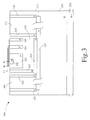
- FIG 3 shows an integrated circuit comprising the structure of Figure 2 and formed with the use of the VIPower process (VIPower is a trade mark of SGS-THOMSON MICROELECTRONICS S.r.l.).
- VIPower is a trade mark of SGS-THOMSON MICROELECTRONICS S.r.l.
- This is a mixed (signal and power) integrated circuit in which both the low-voltage control circuits and the high-voltage power devices are integrated on the same semiconductor chip.
- the semiconductor chip is formed from a semiconductor substrate with a first type of conductivity on which an epitaxial layer doped with the same type of impurities is formed.
- the power transistors (bipolar or field-effect) are constructed with a structure with wholly vertical conduction in which the various P-N junctions are buried in the epitaxial layer; the collector or drain electrode is formed on the back of the chip, that is on the opposite face of the substrate to that with the epitaxial layer.
- the control circuitry on the other hand is formed within one or more wells insulated by means of regions having a second type of conductivity and formed in the epitaxial layer. This construction process is described in European patent application EP-322040 in the name of SGS-THOMSON MICROELECTRONICS S.r.l.
- a first epitaxial layer 310 is formed by epitaxial growth on a substrate 305 of monocrystalline silicon strongly doped with N-type impurities (N+), the epitaxial layer 310 having the same type of conductivity N but with a low concentration of impurities (N-).
- P-type regions having an intermediate concentration of impurities (P) are formed by implantation on the surface of the epitaxial layer 310; regions with N-type doping are then formed on these P-type regions by a subsequent implantation step.
- a second, N-type epitaxial layer 315 having a concentration of impurities greater than or equal to that of the first layer 310 is formed thereon by epitaxial growth.
- the implanted P-type and N-type regions described above extend by diffusion into the two epitaxial layers 310 and 315 giving rise to buried regions.
- the P-type region 320 forms a buried insulation region for an N-type well
- the N-type region 325 constitutes a buried collector region of the low-voltage NPN transistor Ti.
- P-type regions having high concentrations of impurities are then formed in the second epitaxial layer 315 by known masking and diffusion techniques and extend through the entire second epitaxial layer.
- the P-type region 330 is connected to the buried P-type region 320 to complete the insulation region which defines an insulated N-type well.
- the P-type regions 335 and 340 are connected to the same buried P-type region 320, subdividing the insulated N-type well described above into a plurality of cells 349, 350 and 351 insulated from one another.
- an N-type region 345 with a high concentration of impurities is formed by implantation techniques (or alternatively by a deposition process) and diffusion techniques and extends into the second epitaxial layer 315 as far as the respective buried collector region 325 to form a deep collector contact of the vertical NPN transistor Ti.
- P-type regions are then implanted and diffused into the insulated cell 350 by similar techniques.
- the P-type region 355 defines the base region of the vertical NPN transistor Ti and the P-type regions 360 and 365 define the resistors R1i and R2i, respectively.
- a further high-concentration N-type region 370 is formed by implantation and diffusion within the region 355 and defines the emitter region of the vertical NPN transistor.
- Metal strips are then formed by known deposition, masking and etching techniques, in contact with surface regions of the various components, on the front face of the chip, which is coated with a layer of silicon dioxide (not shown in the drawing).
- the two terminals of the resistor R1i are connected to the emitter terminal (Ei) and to the base terminal (Bi) of the transistor Ti, respectively; similarly, the two terminals of the resistor R2i are connected to the collector terminal (Ci) of the transistor Ti and to the same base terminal (Bi).
- each of the two resistors R1i and R2i integrated in the insulated N-type well 350 creates a parasitic PNP transistor defined by the P-type region 360 or 365, by the N-type well 350 and the buried N region 325, and by the buried P insulation region 320.
- the collector terminal of the transistor Ti, and hence the buried N-type region 325 is conductive at a higher potential than that of the other regions constituting the Vbe multiplier in question, this parasitic transistor is always cut off so that the two resistors R1i and R2i thus integrated in the N-type well 350 do not activate any parasitic components.
- Vbe multipliers can be integrated in respective insulated cells within a single P-type insulation region.
- the number of Vbe multipliers which can be integrated in the same insulated well depends upon the breakdown voltage of the P-N junction between the buried insulation region 320 and the buried collector regions (for example, the region 325) of the various low-voltage transistors (typically below 50V).
- the P-N junction described above in fact has to be polarized in reverse; the buried P-type insulation region 320 is therefore connected (by means of the region 330) to the terminal with the lowest potential present within it, that is, the emitter terminal of the transistor constituting the first Vbe multiplier.
- the voltage produced by the series of Vbe multipliers integrated within the insulated well is supplied between the emitter terminal of the first transistor (connected as mentioned above to the buried insulation region 320) and the collector terminal of the last transistor (connected to a buried N-type region in contact with the buried insulation region 320).
- the voltage supplied by the series of Vbe multipliers integrated within the same insulated well cannot exceed the breakdown voltage of the P-N junction formed between the buried P-type insulation region 320 and the buried N-type collector region of the last transistor.
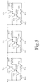
- FIG. 4 this is a circuit diagram corresponding to a different embodiment of the present invention using stages in a Darlington configuration.
- the thermal compensation device shown in the drawing is constituted by a series of n Vbe multipliers, each comprising two low-voltage transistors having a common collector, the emitter of one transistor being connected directly to the base of the other transistor.
- the resistor R1i is connected between an emitter terminal of a first low-voltage transistor T1i and a base terminal of a second low-voltage transistor T2i and the second resistor R2i is connected between a collector terminal of the first transistor T1i and the same base terminal of the transistor T2i.
- the collector terminal of the transistor T1i is connected to a collector terminal of the transistor T2i; the transistor T1i also has a base terminal connected to an emitter terminal of the transistor T2i.
- each Vbe multiplier also includes an "anti-leakage" resistor.
- resistor R3i connected between the base terminal and the emitter terminal of the transistor T1i.
- currents may in fact arise due to structural leakages; in particular, the current injected into the base terminal of the transistor T1i may cause undesired switching-on thereof.
- the resistor R3i connected between the base and emitter terminals of the transistor T1i enables this current to be "shunted”; if the resistor R3i is of a size such that the voltage drop therein is always less than the threshold voltage Vbe of the transistor T1i, undesired switching-on of the transistor is prevented.
- Typical values of the resistances of these "anti-leakage" resistors are from a few hundreds of ⁇ to a few tens of k ⁇ .
- the three transistors T1i, T2i and T3i are connected in a Darlington configuration, that is, with a common collector and with the emitter of one transistor connected directly to the base of the next transistor; the first resistor R1i is connected between an emitter terminal of the transistor T1i and a base terminal of the transistor T3i and the second resistor R2i is connected between a collector terminal of the transistor T1i and the same base terminal of the transistor T3i.
- respective "anti-leakage" resistors R3i and R4i are connected between the base and emitter terminals of the transistors T1i and T2i, to prevent undesired switching-on of these transistors because of currents caused by structural leakages of the circuit.
- thermal compensation device can be also be formed in a manner similar to that described above, with Vbe multipliers comprising 4 or more transistors in a Darlington configuration.
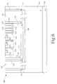
- FIG. 6 An integrated circuit comprising the structure of Figure 5 is shown in Figure 6.
- the integrated circuit 600 shown in the drawing is formed on an N+ substrate 305 on which an N epitaxial layer 310-315 is grown.
- An insulated well is formed within the epitaxial layer 310-315 by means of a P-type insulation region (constituted by a buried region 320 and a contact region 330) and is subdivided into a plurality of insulated cells by means of P-type regions 335 and 340.
- the low-voltage transistors T1i, T2i and T3i and the resistors R1i, R2i, R3i and R4i are shown in an insulated cell 350.
- this insulated cell 350 there is a buried N-type region 325 and an N-type region 345 which extends from the surface of the chip to contact the buried region 325; the N-type region 325 constitutes the buried collector region of the three transistors T1i, T2i and T3i.
- the base regions of the transistors T1i, T2i and T3i constituted by respective P-type regions 610, 615 and 620.
- the emitter regions of the transistors T1i, T2i and T3i, formed by respective N-type regions 625, 630 and 635, are formed within the P-type regions 610, 615 and 620.
- the resistors R1i, R2i, R3i and R4i are formed by respective P-type regions 640, 645, 650 and 655 formed within the insulated well 350 which is common to the three transistors T1i, T2i and T3i.
- the various components of the integrated circuit are suitably interconnected by means of surface metal contacts (not shown in the drawing).
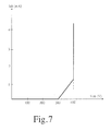
- FIG. 7 shows graphically the voltage-current characteristic of a Zener chain compensated for temperature by means of the device according to the present invention.
- the graph shows the variation of the current Iab (in mA) between the two terminals of the device (Zener chain plus Vbe multipliers) as a function of the voltage Vab (in V) applied to the same terminals; the foregoing numerical example is considered, in which, of a total voltage of 400V, 300V is supplied by the Zener chain and 100V by the thermal compensation device.
- the entire device is non-conductive so that the current lab is zero.
- the Zener chain becomes conductive and a current starts to flow through the resistive path formed by the various resistors present in the thermal compensation device, the transistors of which are still cut off.
- a resistive path is formed by the series of resistors R11-R2n. It will be noted that this current has to be small enough (a few mA) not to create malfunctions in the circuit; for example, if this circuit is used in the electronic-ignition integrated circuit described at the beginning, this current has to be small enough not to switch the power transistor on again.
- the transistors constituting the series of Vbe multipliers become conductive so that the voltage is kept substantially constant irrespective of the current Iab.
Landscapes
- Bipolar Integrated Circuits (AREA)
- Semiconductor Integrated Circuits (AREA)
Claims (8)
- Eine monolithische integrierte Halbleiterschaltung, die in einem Chip (300) eines Halbleitermaterials (310-315) mit einem ersten Leitfähigkeitstyp gebildet ist, wobei die Schaltung eine Hochspannungsvorrichtung (210) mit einer vorbestimmten Rückwärtsleitungsschwelle und eine Wärmekompensationsvorrichtung (250) für die Rückwärtsleitungsschwellenvorrichtung (210), die mit derselben in Reihe geschaltet ist, aufweist, dadurch gekennzeichnet, daß
die Wärmekompensationsvorrichtung (250) eine Mehrzahl von Niedrigspannungs-Vbe-Multiplizierern aufweist, die miteinander in Reihe geschaltet sind, und der Chip (300) eine Mehrzahl von Mulden mit dem ersten Leitfähigkeitstyp aufweist, die mittels eines ersten vergrabenen Bereichs (320) mit einem zweiten Leitfähigkeitstyp und mittels eines ersten Kontaktbereichs (330) mit dem zweiten Leitfähigkeitstyp, der sich von einer Oberfläche des Chips (300) erstreckt, um den ersten vergrabenen Bereich (320) zu berühren, isoliert sind, wobei jede Mulde in eine Mehrzahl von Zellen (349, 350, 351) unterteilt ist, die mittels weiterer Kontaktbereiche (335, 340) mit dem zweiten Leitfähigkeitstyp, die sich von der Oberfläche erstrecken, um den ersten vergrabenen Bereich (320) zu berühren, voneinander isoliert sind, wobei jeder Vbe-Multiplizierer in einer entsprechenden der Zellen gebildet ist, und wobei jeder der Vbe-Multiplizierer einen Widerstandsteiler (R1i, R2i), der aus einem ersten und einem zweiten Widerstand (R1i, R2i) besteht, die zwischen einen ersten Anschluß (Ei) und einen zweiten Anschluß (Ci) des Vbe-Multiplizierers in Reihe geschaltet sind, und einen ersten Transistor (Ti) aufweist, der einen Emitteranschluß (Ei) und einen Kollektoranschluß (Ci), die mit dem ersten beziehungsweise dem zweiten Anschluß des Vbe-Multiplizierers verbunden sind, und einen Basisanschluß (Bi), der mit einem Zwischenabgriff des Teilers (R1, R2) verbunden ist, umfaßt. - Eine monolithische integrierte Halbleiterschaltung gemäß Anspruch 1, bei der der Chip (300) ein Substrat (305) mit dem ersten Leitfähigkeitstyp, eine erste Epitaxialschicht (310) mit dem ersten Leitfähigkeitstyp, die auf dem-Substrat (305) aufgewachsen ist, und eine zweite Epitaxialschicht (315) mit dem ersten Leitfähigkeitstyp, die auf der ersten Epitaxialschicht (310) aufgewachsen ist, umfaßt, wobei jeder erste vergrabene Bereich (320) zwischen der ersten (310) und der zweiten (315) Epitaxialschicht vergraben ist.
- Eine monolithische integrierte Halbleiterschaltung gemäß Anspruch 1 oder 2, bei der jede der Zellen einen zweiten vergrabenen Bereich (325) mit dem ersten Leitfähigkeitstyp, der eine vergrabene Verbindung mit dem ersten vergrabenen Bereich (320) bildet, und einen zweiten Kontaktbereich (345) mit dem ersten Leitfähigkeitstyp, der sich von der Oberfläche erstreckt, um den zweiten vergrabenen Bereich (325) zu berühren, aufweist, wobei sich ein erster Bereich (355) mit dem zweiten Leitfähigkeitstyp von der Oberfläche in die Zelle (350) erstreckt, und sich ein zweiter Bereich (370) mit dem ersten Leitfähigkeitstyp von der Oberfläche in den ersten Bereich (355) erstreckt, wobei die Zelle (350), der erste Bereich (355) und der zweite Bereich (370) die Kollektor-, Basis- beziehungsweise Emitterbereiche des ersten Transistors (Ti) bilden, und wobei sich ein dritter Bereich (360) und ein vierter Bereich (365) mit dem zweiten Leitfähigkeitstyp von der Oberfläche in die Zelle (350) erstrecken und den ersten Widerstand (R1i) bzw. den zweiten Widerstand (R2i) bilden, und wobei bei jeder Mulde der Emitterbereich (370) in einer ersten der Zellen mit dem ersten Kontaktbereich (330) verbunden ist.
- Eine monolithische integrierte Haltleiterschaltung gemäß Anspruch 3, bei der der Basisanschluß des ersten Transistors (T1i) mit dem Zwischenabgriff des Teilers (R1i, R2i) mittels eines zweiten Transistors (T2i) verbunden ist, der einen Emitteranschluß und einen Kollektoranschluß, die mit dem Basisanschluß beziehungsweise dem Kollektoranschluß des ersten Transistors (T1i) verbunden sind, und einen Basisanschluß aufweist, der mit dem Zwischenabgriff des Teilers (R1, R2) verbunden ist, und bei der jede Zelle einen fünften Bereich (615) mit dem zweiten Leitfähigkeitstyp, der sich von der Oberfläche in die Zelle (350) erstreckt, und einen sechsten Bereich (630) mit dem ersten Leitfähigkeitstyp, der sich von der Oberfläche in den fünften Bereich (615) erstreckt, aufweist, wobei die Zelle (350), der fünfte Bereich (615) und der sechste Bereich (630) die Kollektor-, Basis- beziehungsweise Emitterbereiche des zweiten Transistors (T2i) bilden.
- Eine monolithische integrierte Halbleiterschaltung gemäß Anspruch 4, bei der jeder der Vbe-Multiplizierer einen dritten Widerstand (R3i) aufweist, der zwischen den Basisanschluß und den Emitteranschluß des ersten Transistors (T1i) geschaltet ist, und bei der jede Zelle einen siebten Bereich (650) mit dem zweiten Leitfähigkeitstyp aufweist, der sich von der Oberfläche in die Zelle (350) erstreckt und den dritten Widerstand (R3i) bildet.
- Eine monolithische integrierte Halbleiterschaltung gemäß Anspruch 4 oder 5, bei der der Basisanschluß des zweiten Transistors (T2i) mit dem Zwischenabgriff des Teilers (R1i, R2i) mittels eines dritten Transistors (T3i) verbunden ist, der einen Emitteranschluß und einen Kollektoranschluß, die mit dem Basisanschluß beziehungsweise mit dem Kollektoranschluß des zweiten Transistors (T2i) verbunden sind, und einen Basisanschluß aufweist, der mit dem Zwischenabgriff des Teilers (R1i, R2i) verbunden ist, und bei der jede Zelle einen achten Bereich (620) mit dem zweiten Leitfähigkeitstyp, der sich von der Oberfläche in die Zelle (350) erstreckt, und einen neunten Bereich (635) mit dem ersten Leitfähigkeitstyp, der sich von der Oberfläche in den achten Bereich (620) erstreckt, aufweist, wobei die Zelle (350), der achte Bereich (620) und der neunte Bereich (635) die Kollektor-, Basisbeziehungsweise Emitterbereiche des dritten Transistors (T3i) bilden.
- Eine monolithische integrierte Halbleiterschaltung gemäß Anspruch 6, bei der jeder der Vbe-Multiplizierer einen vierten Widerstand (R4i) aufweist, der zwischen den Basisanschluß und den Emitteranschluß des zweiten Transistors (T2i) geschaltet ist, und bei der jede Zelle einen zehnten Bereich (655) mit dem zweiten Leitfähigkeitstyp aufweist, der sich von der Oberfläche in die Zelle (350) erstreckt und den vierten Widerstand (R4i) bildet.
- Eine monolithische integrierte Halbleiterschaltung gemäß einem der Ansprüche 1 bis 7, bei der die Vorrichtung (210) mit einer vorbestimmten Rückwärtsleitungsschwelle durch eine oder mehr Zener-Dioden gebildet ist, die miteinander in Reihe geschaltet sind.
Priority Applications (4)
| Application Number | Priority Date | Filing Date | Title |
|---|---|---|---|
| DE69618178T DE69618178D1 (de) | 1996-05-14 | 1996-05-14 | Ein integrierter Schaltkreis mit einer Vorrichtung die eine festgelegte Sperrspannungsschwelle und eine Temperaturkompensationsvorrichtung mittels Vbe-Multiplizierer aufweist |
| EP96830276A EP0810503B1 (de) | 1996-05-14 | 1996-05-14 | Ein integrierter Schaltkreis mit einer Vorrichtung die eine festgelegte Sperrspannungsschwelle und eine Temperaturkompensationsvorrichtung mittels Vbe-Multiplizierer aufweist |
| JP9117247A JPH1051011A (ja) | 1996-05-14 | 1997-05-07 | モノリシック半導体集積回路 |
| US08/854,452 US5949122A (en) | 1996-05-14 | 1997-05-12 | Integrated circuit with a device having a predetermined reverse conduction threshold and a thermal compensation device with Vbe multipliers |
Applications Claiming Priority (1)
| Application Number | Priority Date | Filing Date | Title |
|---|---|---|---|
| EP96830276A EP0810503B1 (de) | 1996-05-14 | 1996-05-14 | Ein integrierter Schaltkreis mit einer Vorrichtung die eine festgelegte Sperrspannungsschwelle und eine Temperaturkompensationsvorrichtung mittels Vbe-Multiplizierer aufweist |
Publications (2)
| Publication Number | Publication Date |
|---|---|
| EP0810503A1 EP0810503A1 (de) | 1997-12-03 |
| EP0810503B1 true EP0810503B1 (de) | 2001-12-19 |
Family
ID=8225907
Family Applications (1)
| Application Number | Title | Priority Date | Filing Date |
|---|---|---|---|
| EP96830276A Expired - Lifetime EP0810503B1 (de) | 1996-05-14 | 1996-05-14 | Ein integrierter Schaltkreis mit einer Vorrichtung die eine festgelegte Sperrspannungsschwelle und eine Temperaturkompensationsvorrichtung mittels Vbe-Multiplizierer aufweist |
Country Status (4)
| Country | Link |
|---|---|
| US (1) | US5949122A (de) |
| EP (1) | EP0810503B1 (de) |
| JP (1) | JPH1051011A (de) |
| DE (1) | DE69618178D1 (de) |
Cited By (1)
| Publication number | Priority date | Publication date | Assignee | Title |
|---|---|---|---|---|
| EP3701350A2 (de) * | 2017-10-25 | 2020-09-02 | Schneider Electric Solar Inverters USA, Inc. | Anlaufschaltung |
Families Citing this family (6)
| Publication number | Priority date | Publication date | Assignee | Title |
|---|---|---|---|---|
| SE515836C3 (sv) | 1999-05-17 | 2001-11-06 | Ericsson Telefon Ab L M | Förfarande för tillverkning av en bipolär högfrekvent kiseltransistor samt effekttransistoranordning |
| IT1311309B1 (it) * | 1999-12-10 | 2002-03-12 | St Microelectronics Srl | Resistore verticale integrato ad alta tensione e relativo processo difabbricazione. |
| US6222350B1 (en) | 2000-01-21 | 2001-04-24 | Titan Specialties, Ltd. | High temperature voltage regulator circuit |
| US6713991B1 (en) | 2002-04-24 | 2004-03-30 | Rantec Power Systems Inc. | Bipolar shunt regulator |
| DE10301586B3 (de) * | 2003-01-17 | 2004-02-26 | Micronas Gmbh | Integrierte Schaltung |
| US7508096B1 (en) * | 2007-09-20 | 2009-03-24 | General Electric Company | Switching circuit apparatus having a series conduction path for servicing a load and switching method |
Family Cites Families (7)
| Publication number | Priority date | Publication date | Assignee | Title |
|---|---|---|---|---|
| NL6705024A (de) * | 1967-04-08 | 1968-10-09 | ||
| US3723776A (en) * | 1971-12-27 | 1973-03-27 | Us Navy | Temperature compensated zener diode circuit |
| US3953254A (en) * | 1972-11-07 | 1976-04-27 | Thomson-Csf | Method of producing temperature compensated reference diodes utilizing selective epitaxial growth |
| JPS6048765B2 (ja) * | 1977-12-19 | 1985-10-29 | 日本電気株式会社 | 定電圧半導体集積回路 |
| US4564771A (en) * | 1982-07-17 | 1986-01-14 | Robert Bosch Gmbh | Integrated Darlington transistor combination including auxiliary transistor and Zener diode |
| US4749889A (en) * | 1986-11-20 | 1988-06-07 | Rca Licensing Corporation | Temperature compensation apparatus |
| JPH02210860A (ja) * | 1989-02-09 | 1990-08-22 | Fujitsu Ltd | 半導体集積回路装置 |
-
1996
- 1996-05-14 EP EP96830276A patent/EP0810503B1/de not_active Expired - Lifetime
- 1996-05-14 DE DE69618178T patent/DE69618178D1/de not_active Expired - Lifetime
-
1997
- 1997-05-07 JP JP9117247A patent/JPH1051011A/ja active Pending
- 1997-05-12 US US08/854,452 patent/US5949122A/en not_active Expired - Lifetime
Cited By (1)
| Publication number | Priority date | Publication date | Assignee | Title |
|---|---|---|---|---|
| EP3701350A2 (de) * | 2017-10-25 | 2020-09-02 | Schneider Electric Solar Inverters USA, Inc. | Anlaufschaltung |
Also Published As
| Publication number | Publication date |
|---|---|
| JPH1051011A (ja) | 1998-02-20 |
| US5949122A (en) | 1999-09-07 |
| EP0810503A1 (de) | 1997-12-03 |
| DE69618178D1 (de) | 2002-01-31 |
Similar Documents
| Publication | Publication Date | Title |
|---|---|---|
| US5665994A (en) | Integrated device with a bipolar transistor and a MOSFET transistor in an emitter switching configuration | |
| US5274524A (en) | Programmable protection circuit and its monolithic manufacturing | |
| EP0622849B1 (de) | Monolithisch integrierte Struktur einer elektronischen Vorrichtung mit einer bestimmten unidirektionalen Konduktionsschwellenspannung | |
| KR102728482B1 (ko) | 트랜지스터 및 다이오드를 포함하는 회로 및 소자 | |
| US3596115A (en) | Integrated monolithic semiconductor voltage regulator arrangement | |
| US7075123B2 (en) | Semiconductor input protection circuit | |
| US5347185A (en) | Protection structure against latch-up in a CMOS circuit | |
| US5949122A (en) | Integrated circuit with a device having a predetermined reverse conduction threshold and a thermal compensation device with Vbe multipliers | |
| US3427512A (en) | Semiconductor low voltage switch | |
| JPH0136347B2 (de) | ||
| US4868703A (en) | Solid state switching device | |
| US4577211A (en) | Integrated circuit and method for biasing an epitaxial layer | |
| US4807009A (en) | Lateral transistor | |
| US6127723A (en) | Integrated device in an emitter-switching configuration | |
| CA1183278A (en) | Integrated circuit power transistor array | |
| EP0225586A1 (de) | Überspannungsschutzvorrichtung für MOS-integrierte Schaltungsanordnung | |
| EP0089091A2 (de) | Spannungsverschieber | |
| US5652455A (en) | Integrated structure circuit for the protection of power devices against overvoltage | |
| JPH02226808A (ja) | 過電流保護機能付きパワーmosfet | |
| CN108550573B (zh) | 静电保护器件及其制造方法 | |
| US6020623A (en) | Integrated structure with device having a preset reverse conduction threshold | |
| US4814852A (en) | Controlled voltage drop diode | |
| US4180749A (en) | Input buffer for integrated injection logic circuits | |
| US5751052A (en) | Inductive driver circuit and method therefor | |
| US5986290A (en) | Silicon controlled rectifier with reduced substrate current |
Legal Events
| Date | Code | Title | Description |
|---|---|---|---|
| PUAI | Public reference made under article 153(3) epc to a published international application that has entered the european phase |
Free format text: ORIGINAL CODE: 0009012 |
|
| 17P | Request for examination filed |
Effective date: 19970325 |
|
| AK | Designated contracting states |
Kind code of ref document: A1 Designated state(s): DE FR GB IT |
|
| 17Q | First examination report despatched |
Effective date: 19990908 |
|
| GRAG | Despatch of communication of intention to grant |
Free format text: ORIGINAL CODE: EPIDOS AGRA |
|
| GRAG | Despatch of communication of intention to grant |
Free format text: ORIGINAL CODE: EPIDOS AGRA |
|
| GRAH | Despatch of communication of intention to grant a patent |
Free format text: ORIGINAL CODE: EPIDOS IGRA |
|
| GRAH | Despatch of communication of intention to grant a patent |
Free format text: ORIGINAL CODE: EPIDOS IGRA |
|
| GRAA | (expected) grant |
Free format text: ORIGINAL CODE: 0009210 |
|
| AK | Designated contracting states |
Kind code of ref document: B1 Designated state(s): DE FR GB IT |
|
| PG25 | Lapsed in a contracting state [announced via postgrant information from national office to epo] |
Ref country code: FR Free format text: LAPSE BECAUSE OF FAILURE TO SUBMIT A TRANSLATION OF THE DESCRIPTION OR TO PAY THE FEE WITHIN THE PRESCRIBED TIME-LIMIT Effective date: 20011219 |
|
| REG | Reference to a national code |
Ref country code: GB Ref legal event code: IF02 |
|
| REF | Corresponds to: |
Ref document number: 69618178 Country of ref document: DE Date of ref document: 20020131 |
|
| PG25 | Lapsed in a contracting state [announced via postgrant information from national office to epo] |
Ref country code: DE Free format text: LAPSE BECAUSE OF FAILURE TO SUBMIT A TRANSLATION OF THE DESCRIPTION OR TO PAY THE FEE WITHIN THE PRESCRIBED TIME-LIMIT Effective date: 20020320 |
|
| EN | Fr: translation not filed | ||
| PLBE | No opposition filed within time limit |
Free format text: ORIGINAL CODE: 0009261 |
|
| STAA | Information on the status of an ep patent application or granted ep patent |
Free format text: STATUS: NO OPPOSITION FILED WITHIN TIME LIMIT |
|
| 26N | No opposition filed | ||
| PG25 | Lapsed in a contracting state [announced via postgrant information from national office to epo] |
Ref country code: IT Free format text: LAPSE BECAUSE OF NON-PAYMENT OF DUE FEES;WARNING: LAPSES OF ITALIAN PATENTS WITH EFFECTIVE DATE BEFORE 2007 MAY HAVE OCCURRED AT ANY TIME BEFORE 2007. THE CORRECT EFFECTIVE DATE MAY BE DIFFERENT FROM THE ONE RECORDED. Effective date: 20050514 |
|
| PGFP | Annual fee paid to national office [announced via postgrant information from national office to epo] |
Ref country code: GB Payment date: 20070427 Year of fee payment: 12 |
|
| GBPC | Gb: european patent ceased through non-payment of renewal fee |
Effective date: 20080514 |
|
| PG25 | Lapsed in a contracting state [announced via postgrant information from national office to epo] |
Ref country code: GB Free format text: LAPSE BECAUSE OF NON-PAYMENT OF DUE FEES Effective date: 20080514 |