EP0810655A2 - Paquetage pour un dispositif semi-conducteur - Google Patents
Paquetage pour un dispositif semi-conducteur Download PDFInfo
- Publication number
- EP0810655A2 EP0810655A2 EP97303638A EP97303638A EP0810655A2 EP 0810655 A2 EP0810655 A2 EP 0810655A2 EP 97303638 A EP97303638 A EP 97303638A EP 97303638 A EP97303638 A EP 97303638A EP 0810655 A2 EP0810655 A2 EP 0810655A2
- Authority
- EP
- European Patent Office
- Prior art keywords
- integrated circuit
- package
- circuit board
- hole
- sealing material
- Prior art date
- Legal status (The legal status is an assumption and is not a legal conclusion. Google has not performed a legal analysis and makes no representation as to the accuracy of the status listed.)
- Withdrawn
Links
Images


Classifications
-
- H—ELECTRICITY
- H10—SEMICONDUCTOR DEVICES; ELECTRIC SOLID-STATE DEVICES NOT OTHERWISE PROVIDED FOR
- H10W—GENERIC PACKAGES, INTERCONNECTIONS, CONNECTORS OR OTHER CONSTRUCTIONAL DETAILS OF DEVICES COVERED BY CLASS H10
- H10W90/00—Package configurations
- H10W90/701—Package configurations characterised by the relative positions of pads or connectors relative to package parts
-
- H—ELECTRICITY
- H10—SEMICONDUCTOR DEVICES; ELECTRIC SOLID-STATE DEVICES NOT OTHERWISE PROVIDED FOR
- H10W—GENERIC PACKAGES, INTERCONNECTIONS, CONNECTORS OR OTHER CONSTRUCTIONAL DETAILS OF DEVICES COVERED BY CLASS H10
- H10W70/00—Package substrates; Interposers; Redistribution layers [RDL]
- H10W70/40—Leadframes
- H10W70/411—Chip-supporting parts, e.g. die pads
- H10W70/415—Leadframe inner leads serving as die pads
-
- H—ELECTRICITY
- H10—SEMICONDUCTOR DEVICES; ELECTRIC SOLID-STATE DEVICES NOT OTHERWISE PROVIDED FOR
- H10W—GENERIC PACKAGES, INTERCONNECTIONS, CONNECTORS OR OTHER CONSTRUCTIONAL DETAILS OF DEVICES COVERED BY CLASS H10
- H10W74/00—Encapsulations, e.g. protective coatings
-
- H—ELECTRICITY
- H10—SEMICONDUCTOR DEVICES; ELECTRIC SOLID-STATE DEVICES NOT OTHERWISE PROVIDED FOR
- H10W—GENERIC PACKAGES, INTERCONNECTIONS, CONNECTORS OR OTHER CONSTRUCTIONAL DETAILS OF DEVICES COVERED BY CLASS H10
- H10W74/00—Encapsulations, e.g. protective coatings
- H10W74/10—Encapsulations, e.g. protective coatings characterised by their shape or disposition
- H10W74/111—Encapsulations, e.g. protective coatings characterised by their shape or disposition the semiconductor body being completely enclosed
- H10W74/129—Encapsulations, e.g. protective coatings characterised by their shape or disposition the semiconductor body being completely enclosed forming a chip-scale package [CSP]
-
- H—ELECTRICITY
- H10—SEMICONDUCTOR DEVICES; ELECTRIC SOLID-STATE DEVICES NOT OTHERWISE PROVIDED FOR
- H10W—GENERIC PACKAGES, INTERCONNECTIONS, CONNECTORS OR OTHER CONSTRUCTIONAL DETAILS OF DEVICES COVERED BY CLASS H10
- H10W72/00—Interconnections or connectors in packages
- H10W72/071—Connecting or disconnecting
- H10W72/073—Connecting or disconnecting of die-attach connectors
- H10W72/07351—Connecting or disconnecting of die-attach connectors characterised by changes in properties of the die-attach connectors during connecting
- H10W72/07352—Connecting or disconnecting of die-attach connectors characterised by changes in properties of the die-attach connectors during connecting changes in structures or sizes
-
- H—ELECTRICITY
- H10—SEMICONDUCTOR DEVICES; ELECTRIC SOLID-STATE DEVICES NOT OTHERWISE PROVIDED FOR
- H10W—GENERIC PACKAGES, INTERCONNECTIONS, CONNECTORS OR OTHER CONSTRUCTIONAL DETAILS OF DEVICES COVERED BY CLASS H10
- H10W72/00—Interconnections or connectors in packages
- H10W72/30—Die-attach connectors
- H10W72/321—Structures or relative sizes of die-attach connectors
-
- H—ELECTRICITY
- H10—SEMICONDUCTOR DEVICES; ELECTRIC SOLID-STATE DEVICES NOT OTHERWISE PROVIDED FOR
- H10W—GENERIC PACKAGES, INTERCONNECTIONS, CONNECTORS OR OTHER CONSTRUCTIONAL DETAILS OF DEVICES COVERED BY CLASS H10
- H10W72/00—Interconnections or connectors in packages
- H10W72/50—Bond wires
- H10W72/551—Materials of bond wires
- H10W72/552—Materials of bond wires comprising metals or metalloids, e.g. silver
- H10W72/5522—Materials of bond wires comprising metals or metalloids, e.g. silver comprising gold [Au]
-
- H—ELECTRICITY
- H10—SEMICONDUCTOR DEVICES; ELECTRIC SOLID-STATE DEVICES NOT OTHERWISE PROVIDED FOR
- H10W—GENERIC PACKAGES, INTERCONNECTIONS, CONNECTORS OR OTHER CONSTRUCTIONAL DETAILS OF DEVICES COVERED BY CLASS H10
- H10W72/00—Interconnections or connectors in packages
- H10W72/851—Dispositions of multiple connectors or interconnections
- H10W72/853—On the same surface
- H10W72/865—Die-attach connectors and bond wires
-
- H—ELECTRICITY
- H10—SEMICONDUCTOR DEVICES; ELECTRIC SOLID-STATE DEVICES NOT OTHERWISE PROVIDED FOR
- H10W—GENERIC PACKAGES, INTERCONNECTIONS, CONNECTORS OR OTHER CONSTRUCTIONAL DETAILS OF DEVICES COVERED BY CLASS H10
- H10W72/00—Interconnections or connectors in packages
- H10W72/90—Bond pads, in general
- H10W72/941—Dispositions of bond pads
- H10W72/944—Dispositions of multiple bond pads
- H10W72/9445—Top-view layouts, e.g. mirror arrays
-
- H—ELECTRICITY
- H10—SEMICONDUCTOR DEVICES; ELECTRIC SOLID-STATE DEVICES NOT OTHERWISE PROVIDED FOR
- H10W—GENERIC PACKAGES, INTERCONNECTIONS, CONNECTORS OR OTHER CONSTRUCTIONAL DETAILS OF DEVICES COVERED BY CLASS H10
- H10W74/00—Encapsulations, e.g. protective coatings
- H10W74/10—Encapsulations, e.g. protective coatings characterised by their shape or disposition
- H10W74/131—Encapsulations, e.g. protective coatings characterised by their shape or disposition the semiconductor body being only partially enclosed
- H10W74/142—Encapsulations, e.g. protective coatings characterised by their shape or disposition the semiconductor body being only partially enclosed the encapsulations exposing the passive side of the semiconductor body
-
- H—ELECTRICITY
- H10—SEMICONDUCTOR DEVICES; ELECTRIC SOLID-STATE DEVICES NOT OTHERWISE PROVIDED FOR
- H10W—GENERIC PACKAGES, INTERCONNECTIONS, CONNECTORS OR OTHER CONSTRUCTIONAL DETAILS OF DEVICES COVERED BY CLASS H10
- H10W90/00—Package configurations
- H10W90/701—Package configurations characterised by the relative positions of pads or connectors relative to package parts
- H10W90/731—Package configurations characterised by the relative positions of pads or connectors relative to package parts of die-attach connectors
- H10W90/734—Package configurations characterised by the relative positions of pads or connectors relative to package parts of die-attach connectors between a chip and a stacked insulating package substrate, interposer or RDL
-
- H—ELECTRICITY
- H10—SEMICONDUCTOR DEVICES; ELECTRIC SOLID-STATE DEVICES NOT OTHERWISE PROVIDED FOR
- H10W—GENERIC PACKAGES, INTERCONNECTIONS, CONNECTORS OR OTHER CONSTRUCTIONAL DETAILS OF DEVICES COVERED BY CLASS H10
- H10W90/00—Package configurations
- H10W90/701—Package configurations characterised by the relative positions of pads or connectors relative to package parts
- H10W90/751—Package configurations characterised by the relative positions of pads or connectors relative to package parts of bond wires
- H10W90/754—Package configurations characterised by the relative positions of pads or connectors relative to package parts of bond wires between a chip and a stacked insulating package substrate, interposer or RDL
-
- H—ELECTRICITY
- H10—SEMICONDUCTOR DEVICES; ELECTRIC SOLID-STATE DEVICES NOT OTHERWISE PROVIDED FOR
- H10W—GENERIC PACKAGES, INTERCONNECTIONS, CONNECTORS OR OTHER CONSTRUCTIONAL DETAILS OF DEVICES COVERED BY CLASS H10
- H10W90/00—Package configurations
- H10W90/701—Package configurations characterised by the relative positions of pads or connectors relative to package parts
- H10W90/751—Package configurations characterised by the relative positions of pads or connectors relative to package parts of bond wires
- H10W90/756—Package configurations characterised by the relative positions of pads or connectors relative to package parts of bond wires between a chip and a stacked lead frame, conducting package substrate or heat sink
Definitions
- the present invention relates to semiconductor devices, and more particularly to packaging board on chip (BOC) devices.
- BOC packaging board on chip
- the semiconductor technology has shown a general trend towards the dramatic increase in integrated circuit speed and density. Both of these trends are fueled by a general reduction in device (active element) geometries. As semiconductor devices becomes smaller, the distances between devices on a semiconductor die become smaller, and parasitics (such as parasitic capacitances) and switching currents become smaller. In technologies, such as CMOS, where overall current draw and switching speed characteristics are dominated by the effects of parasitics, the result is a reduction in total power consumption at the same time as switching speed is improved. Overall speed is further improved by the reduction in signal propagation time between active devices (e.g., transistors), resulting from the shorter distances involved. In today's high speed integrated circuitry based on sub-micron geometries, delays in the tens or hundreds of picoseconds can be appreciable.
- integrated circuit dies are diced (cut apart, or singulated) from a semiconductor wafer and are separated into integrated circuit packages which have pins, leads, solder (ball) bumps, or conductive pads by which electrical connections may be made from external systems to the integrated circuit chip. These packages are then typically applied to circuit board assemblies including systems of interconnected integrated circuit chips.
- chip-on-board technology
- integrated circuit dies are bonded directly to die mounting areas on a circuit board substrate, for example, ceramic, fiberglass, etc., and are wire bonded (with thin "bond wires") to traces on the circuit board in areas adjacent to the edges of the dies.
- the present invention reduces inductance that is induced between wires and internal leads. Additionally, the present packaging arrangement provides one package for all applications. The package for the present invention provides short traces leading to favorable impedance coupling. These short wires are designed to reduce electrical impedance important for the operation of high speed devices, such as the synchronous DRAM. Additionally, the present invention eliminates wire shorts to the bus bar and eliminates T/F. Additionally, the present invention eliminates the use of ultra-advance molding equipment development. Additionally, the present invention provides a true chip size package, which leads to improved mapping density. Additionally, the present invention eliminates bent leads. Lastly, the present invention eliminate noise due to cross-talk and improves the delays associated with longer wires.
- the present invention includes a package for an integrated circuit, including a circuit board for mounting the integrated circuit having a first surface and a second surface, a connector device positioned on the first surface of the circuit board for electrically connecting the integrated circuit, and the integrated circuit being positioned on the second surface.
- Fig. 1 illustrates that solder balls 100 are positioned along the longitudinal edges of printed circuit board 122. To provide the maximum spacing between the individual solder balls, the solder balls may be positioned along the outer edges of the printed circuit board 122.
- the number of the solder balls 100 correspond to the number of connections to the semiconductor die 114.
- the semiconductor die 114 which has been previously cut or diced is mounted to the printed circuit board 122 by an attachment apparatus, for example, polymide tape or any adhesive material suitable to attach the semiconductor die 114 to the printed circuit board 122.
- the semiconductor die 114 is the type with connections along the longitudinal axis of the semiconductor die.
- the electrical connection may be positioned along the central axis of the semiconductor die 114.
- the solder balls 100 are connected to the semiconductor die 114 by wires 118 which may be made of material gold and traces (not shown). These wires 118 are attached to the semiconductor die on the side of the semiconductor die 114 that faces or abuts the printed circuit board 122. The wires 118 extend from the semiconductor die 114 through a hole 120 of the printed circuit board and are attached to traces which run along or through the printed circuit board to the solder balls. The hole through the printed circuit board 122 may be positioned at the central longitudinal axis of the printed circuit.
- the semiconductor die 114 and wires 118 are protected from external objects by the elements by sealing material, such as the epoxy resin to form the chip-on-board (COB) semiconductor device.
- top and bottom have no absolute meaning, for purposes of this application, the side of the printed circuit board 122 with the solder balls 100 and away from the semiconductor die 114 is referred to as the top portion while the bottom portion of the printed circuit board 122 is the side opposite to the solder balls 100 and the same side as the semiconductor die 114.
- the sealing material 110 which is formed on the top surface of the printed circuit board 114 to cover the wires 118 and the hole 120 protects the wires and has a general curved shape.
- the bottom sealing material 112 forms between the printed circuit board 122 and the semiconductor die 114 to encapsulate the adhesive means 116 and the wires 118 and further encapsulate the sides of the semiconductor die 114.
- the bottom of the bottom sealing material 112 is approximately flush with the bottom of the semiconductor die 114.
- Fig. 2 illustrates that the top sealing material 110 is formed around the wires 118 and are generally perpendicular to the longitudinal axis of the printed circuit board 122.
- the height of the packaged device is very compact and approximately only 42 mils.
- the wires 118 are very short and eliminate inductance.
- the height between the bottom of the printed circuit board 122 and the bottom of the semiconductor die 114 is approximately 14 mils while the height from the top of the printed circuit board 122 to the top of the solder balls 100 is approximately 20 mils.
- the semiconductor die 114 is spaced approximately 1 to 3 mils from the bottom of the printed circuit board 122 depending on the type of die attached used.
- Fig. 3 illustrates a variation of the package of Figs. 1 and 2, in that the top sealing material 124 has more angular shape with sloping sidewalls.
- the topview of Figure 4 illustrates that the sealing material 124 has an approximately rectangle shape.
- Fig. 5 illustrates that the bottom sealing material 126 is not flush with the bottom of the semiconductor die 114 and entirely encapsulates the semiconductor die 114 including the bottom surface of the semiconductor die 114. This improves the protection of the semiconductor die 114, but increases the overall height to approximately 50 mils.
- Fig. 6 illustrates that the top sealing material is a curved top sealing material 110.
- the overall height of this package is approximately 50 mils.
- Fig. 7 illustrates that the semiconductor die 114 is not enclosed on either the bottom or sides by a sealing material.
- the adhesive material 116 extends from the hole 120 to the outermost side of the printed circuit board 122. This extension of the adhesive material 116 provides a stable mounting platform for the semiconductor die 114.
- the angular top sealing material 124 is used with the extended adhesive material 116.
- the dimensions ot the semiconductor die 114 are approximately the same as the printed circuit board 122 along the longitudinal axis of the printed circuit board 122.
- Fig. 9 illustrates a construction in the form of a structure of the printed circuit board 122 with the solder balls.
- the structure includes a hole 200 formed by etching, ion milling or other suitable process and extends from the top surface of the printed circuit board 122 into the printed circuit board 122 down to and exposing conductor 202.
- Insulating material 204 for example, SIO 2, electrically insulates the walls of the hole 200 from contact with other active semiconductor devices or different wires 118 of the same semiconductor device.
- a conductive plug 206 is deposited in to hole 200 forming a conductive via from the surface of the printed circuit board 122 to the conductor 202.
- Contact 208 is electrically conductive to plug 206 and is formed on the top surface of the printed circuit board.
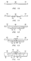
- Figs. 10-14 illustrates a process for the construction of device in accordance with the principals of the present invention.
- a hole 120 is formed along the central longitudinal axis of the printed circuit board 122. Adjacent to the hole 120 and on the bottomside of the printed circuit board 122, adhesive material 116 is placed. Semiconductor die 114 is positioned next on the adhesive means 116 as illustrated in Fig. 12.
- wires 118 are formed from the semiconductor die 114 to the conductors located in the printed circuit board 122 by wire bonding machines (not shown). As illustrated in Fig. 14, a top sealing material 124 protects the wires while a bottom sealing material 126 protects the semiconductor die. These top and bottom sealing materials are formed by molding machine (not shown).
- the wires are very short and eliminate inductance resulting from longer wires and provides favorable impedance and coupling to the semiconductor die. Furthermore, no bus bar is needed.
- the present invention further eliminates or minimizes bent leads resulting from the wire placement process.
Landscapes
- Structures Or Materials For Encapsulating Or Coating Semiconductor Devices Or Solid State Devices (AREA)
- Wire Bonding (AREA)
- Lead Frames For Integrated Circuits (AREA)
- Structures For Mounting Electric Components On Printed Circuit Boards (AREA)
Applications Claiming Priority (2)
| Application Number | Priority Date | Filing Date | Title |
|---|---|---|---|
| US1857996P | 1996-05-29 | 1996-05-29 | |
| US18579P | 1996-05-29 |
Publications (2)
| Publication Number | Publication Date |
|---|---|
| EP0810655A2 true EP0810655A2 (fr) | 1997-12-03 |
| EP0810655A3 EP0810655A3 (fr) | 1999-10-06 |
Family
ID=21788669
Family Applications (1)
| Application Number | Title | Priority Date | Filing Date |
|---|---|---|---|
| EP97303638A Withdrawn EP0810655A3 (fr) | 1996-05-29 | 1997-05-29 | Paquetage pour un dispositif semi-conducteur |
Country Status (4)
| Country | Link |
|---|---|
| US (1) | US6667560B2 (fr) |
| EP (1) | EP0810655A3 (fr) |
| JP (1) | JPH1092972A (fr) |
| KR (1) | KR970077545A (fr) |
Cited By (16)
| Publication number | Priority date | Publication date | Assignee | Title |
|---|---|---|---|---|
| DE19954888A1 (de) * | 1999-11-15 | 2001-05-23 | Infineon Technologies Ag | Verpackung für einen Halbleiterchip |
| DE10024376A1 (de) * | 2000-05-17 | 2001-12-06 | Infineon Technologies Ag | Halbleiterbauelement und Verfahren zu dessen Herstellung |
| EP1205973A1 (fr) * | 2000-11-10 | 2002-05-15 | United Test Center Inc. | Dispositif semi-conducteur à profil plat et procédé de sa fabrication |
| DE10127010A1 (de) * | 2001-06-05 | 2002-12-12 | Infineon Technologies Ag | Elektronisches Bauteil mit einem Halbleiterchip |
| DE10127009A1 (de) * | 2001-06-05 | 2002-12-12 | Infineon Technologies Ag | Kunststoffgehäuse mit mehreren Halbleiterchips und einer Umverdrahtungsplatte sowie ein Verfahren zur Herstellung des Kunststoffgehäuses in einer Spritzgußform |
| DE10152694A1 (de) * | 2001-10-19 | 2003-01-02 | Infineon Technologies Ag | Elektronisches Bauteil mit wenigstens einem Halbleiterchip und einem Kunststoffgehäuse und Verfahren zu seiner Herstellung |
| DE10154199A1 (de) * | 2001-11-07 | 2003-02-06 | Infineon Technologies Ag | Elektronisches Bauteil mit Halbleiterchip und Systemträger mit Bauteilpositionen und Verfahren zu deren Herstellung |
| US6545366B2 (en) | 2001-01-11 | 2003-04-08 | Mitsubishi Denki Kabushiki Kaisha | Multiple chip package semiconductor device |
| WO2000048444A3 (fr) * | 1999-02-16 | 2003-05-22 | Wichmann Workx Ag Information | Boitier pour plaquette a semi-conducteur |
| WO2002091466A3 (fr) * | 2001-05-10 | 2003-06-05 | Koninkl Philips Electronics Nv | Fixation amelioree de puce sur un substrat |
| DE10238581A1 (de) * | 2002-08-22 | 2004-03-11 | Infineon Technologies Ag | Halbleiterbauelement |
| DE10327515A1 (de) * | 2003-06-17 | 2005-01-20 | Infineon Technologies Ag | Substratbasiertes IC-Package |
| EP0993043A3 (fr) * | 1998-09-29 | 2005-08-24 | Texas Instruments Incorporated | Empaquetage de semiconducteur et son procédé de fabrication |
| EP0967647A3 (fr) * | 1998-06-22 | 2005-09-21 | Fujitsu Limited | Procédé de scellage d'un dispositif semiconducteur empaqueté pour montage en surface |
| US6949820B2 (en) | 2003-06-02 | 2005-09-27 | Infineon Technologies Ag | Substrate-based chip package |
| US7042070B2 (en) | 1999-09-22 | 2006-05-09 | Texas Instruments Incorporated | Direct attachment of semiconductor chip to organic substrate |
Families Citing this family (13)
| Publication number | Priority date | Publication date | Assignee | Title |
|---|---|---|---|---|
| US6861290B1 (en) * | 1995-12-19 | 2005-03-01 | Micron Technology, Inc. | Flip-chip adaptor package for bare die |
| US6791194B1 (en) * | 1996-05-30 | 2004-09-14 | Hitachi, Ltd. | Circuit tape having adhesive film, semiconductor device, and a method for manufacturing the same |
| JPH1140694A (ja) | 1997-07-16 | 1999-02-12 | Oki Electric Ind Co Ltd | 半導体パッケージおよび半導体装置とその製造方法 |
| US6890796B1 (en) | 1997-07-16 | 2005-05-10 | Oki Electric Industry Co., Ltd. | Method of manufacturing a semiconductor package having semiconductor decice mounted thereon and elongate opening through which electodes and patterns are connected |
| USRE43112E1 (en) * | 1998-05-04 | 2012-01-17 | Round Rock Research, Llc | Stackable ball grid array package |
| US6577004B1 (en) * | 2000-08-31 | 2003-06-10 | Micron Technology, Inc. | Solder ball landpad design to improve laminate performance |
| JP2002270762A (ja) * | 2001-03-09 | 2002-09-20 | Sony Corp | 半導体装置 |
| US6657132B2 (en) * | 2001-03-15 | 2003-12-02 | Micron Technology, Inc. | Single sided adhesive tape for compound diversion on BOC substrates |
| US7202556B2 (en) * | 2001-12-20 | 2007-04-10 | Micron Technology, Inc. | Semiconductor package having substrate with multi-layer metal bumps |
| US7550842B2 (en) * | 2002-12-12 | 2009-06-23 | Formfactor, Inc. | Integrated circuit assembly |
| JP4334542B2 (ja) * | 2003-08-28 | 2009-09-30 | 富士通株式会社 | パッケージ構造 |
| US7453141B2 (en) | 2005-02-18 | 2008-11-18 | Shinko Electric Industries Co., Ltd. | Semiconductor device package, method of manufacturing the same, and semiconductor device |
| TWI504279B (zh) | 2011-12-01 | 2015-10-11 | 財團法人工業技術研究院 | Mems音波感測器及其製造方法 |
Family Cites Families (46)
| Publication number | Priority date | Publication date | Assignee | Title |
|---|---|---|---|---|
| US3179913A (en) | 1962-01-25 | 1965-04-20 | Ind Electronic Hardware Corp | Rack with multilayer matrix boards |
| US3370203A (en) | 1965-07-19 | 1968-02-20 | United Aircraft Corp | Integrated circuit modules |
| US3459998A (en) | 1967-08-15 | 1969-08-05 | Bell Telephone Labor Inc | Modular circuit assembly |
| US3904934A (en) | 1973-03-26 | 1975-09-09 | Massachusetts Inst Technology | Interconnection of planar electronic structures |
| US4288841A (en) | 1979-09-20 | 1981-09-08 | Bell Telephone Laboratories, Incorporated | Double cavity semiconductor chip carrier |
| US4646128A (en) | 1980-09-16 | 1987-02-24 | Irvine Sensors Corporation | High-density electronic processing package--structure and fabrication |
| US4502098A (en) | 1981-02-10 | 1985-02-26 | Brown David F | Circuit assembly |
| JPS58178529A (ja) | 1982-04-13 | 1983-10-19 | Mitsubishi Electric Corp | 混成集積回路装置 |
| US4574331A (en) | 1983-05-31 | 1986-03-04 | Trw Inc. | Multi-element circuit construction |
| US5019945A (en) | 1983-05-31 | 1991-05-28 | Trw Inc. | Backplane interconnection system |
| US4727410A (en) | 1983-11-23 | 1988-02-23 | Cabot Technical Ceramics, Inc. | High density integrated circuit package |
| JPS61111561A (ja) | 1984-10-05 | 1986-05-29 | Fujitsu Ltd | 半導体装置 |
| US4868712A (en) | 1987-02-04 | 1989-09-19 | Woodman John K | Three dimensional integrated circuit package |
| US4862249A (en) | 1987-04-17 | 1989-08-29 | Xoc Devices, Inc. | Packaging system for stacking integrated circuits |
| US4953005A (en) | 1987-04-17 | 1990-08-28 | Xoc Devices, Inc. | Packaging system for stacking integrated circuits |
| US5016138A (en) | 1987-10-27 | 1991-05-14 | Woodman John K | Three dimensional integrated circuit package |
| US4833568A (en) | 1988-01-29 | 1989-05-23 | Berhold G Mark | Three-dimensional circuit component assembly and method corresponding thereto |
| DE3911711A1 (de) | 1989-04-10 | 1990-10-11 | Ibm | Modul-aufbau mit integriertem halbleiterchip und chiptraeger |
| US5091251A (en) | 1989-05-29 | 1992-02-25 | Tomoegawa Paper Co., Ltd. | Adhesive tapes and semiconductor devices |
| US5148265A (en) | 1990-09-24 | 1992-09-15 | Ist Associates, Inc. | Semiconductor chip assemblies with fan-in leads |
| US5227232A (en) | 1991-01-23 | 1993-07-13 | Lim Thiam B | Conductive tape for semiconductor package, a lead frame without power buses for lead on chip package, and a semiconductor device with conductive tape power distribution |
| FR2675632B1 (fr) | 1991-04-18 | 1997-04-30 | Texas Instruments France | Dispositif de conditionnement de circuits integres |
| US5239448A (en) | 1991-10-28 | 1993-08-24 | International Business Machines Corporation | Formulation of multichip modules |
| US5491362A (en) | 1992-04-30 | 1996-02-13 | Vlsi Technology, Inc. | Package structure having accessible chip |
| US5336928A (en) | 1992-09-18 | 1994-08-09 | General Electric Company | Hermetically sealed packaged electronic system |
| JP3267409B2 (ja) | 1992-11-24 | 2002-03-18 | 株式会社日立製作所 | 半導体集積回路装置 |
| US5479319A (en) | 1992-12-30 | 1995-12-26 | Interconnect Systems, Inc. | Multi-level assemblies for interconnecting integrated circuits |
| US5444296A (en) | 1993-11-22 | 1995-08-22 | Sun Microsystems, Inc. | Ball grid array packages for high speed applications |
| US5384689A (en) | 1993-12-20 | 1995-01-24 | Shen; Ming-Tung | Integrated circuit chip including superimposed upper and lower printed circuit boards |
| JPH07288385A (ja) | 1994-04-19 | 1995-10-31 | Hitachi Chem Co Ltd | 多層配線板及びその製造法 |
| JP2833996B2 (ja) * | 1994-05-25 | 1998-12-09 | 日本電気株式会社 | フレキシブルフィルム及びこれを有する半導体装置 |
| JP3146849B2 (ja) | 1994-05-27 | 2001-03-19 | 松下電器産業株式会社 | 電子部品および電子部品の製造方法 |
| US5889333A (en) | 1994-08-09 | 1999-03-30 | Fujitsu Limited | Semiconductor device and method for manufacturing such |
| IT1272817B (it) | 1994-08-24 | 1997-06-30 | Consorzio Eagle | Procedimento per il montaggio di circuiti integrati su pannelli di circuiti stampati |
| DE9417734U1 (de) | 1994-11-08 | 1995-03-16 | Zentrum Mikroelektronik Dresden GmbH, 01109 Dresden | Halbleiteranordnung für Chip-Module |
| JP3487524B2 (ja) * | 1994-12-20 | 2004-01-19 | 株式会社ルネサステクノロジ | 半導体装置及びその製造方法 |
| US5677566A (en) * | 1995-05-08 | 1997-10-14 | Micron Technology, Inc. | Semiconductor chip package |
| KR0144164B1 (ko) | 1995-05-12 | 1998-07-01 | 문정환 | 엘오씨 반도체 패키지 및 반도체 장치를 패키징하는 방법 |
| JP2970491B2 (ja) | 1995-09-20 | 1999-11-02 | ソニー株式会社 | 半導体パッケージ及びその製造方法 |
| US5834336A (en) | 1996-03-12 | 1998-11-10 | Texas Instruments Incorporated | Backside encapsulation of tape automated bonding device |
| US5731542A (en) | 1996-05-23 | 1998-03-24 | Motorola, Inc. | Apparatus and method for mounting an electronic component to a substrate and method for spray-cooling an electronic component mounted to a substrate |
| US5784260A (en) | 1996-05-29 | 1998-07-21 | International Business Machines Corporation | Structure for constraining the flow of encapsulant applied to an I/C chip on a substrate |
| KR19980020726A (ko) | 1996-09-11 | 1998-06-25 | 김광호 | 칩 스케일의 볼 그리드 어레이 패키지 및 그의 제조 방법 |
| US5866949A (en) | 1996-12-02 | 1999-02-02 | Minnesota Mining And Manufacturing Company | Chip scale ball grid array for integrated circuit packaging |
| US5798567A (en) | 1997-08-21 | 1998-08-25 | Hewlett-Packard Company | Ball grid array integrated circuit package which employs a flip chip integrated circuit and decoupling capacitors |
| US6049129A (en) | 1997-12-19 | 2000-04-11 | Texas Instruments Incorporated | Chip size integrated circuit package |
-
1997
- 1997-05-27 US US08/863,848 patent/US6667560B2/en not_active Expired - Lifetime
- 1997-05-28 KR KR1019970021301A patent/KR970077545A/ko not_active Withdrawn
- 1997-05-28 JP JP9138446A patent/JPH1092972A/ja active Pending
- 1997-05-29 EP EP97303638A patent/EP0810655A3/fr not_active Withdrawn
Cited By (24)
| Publication number | Priority date | Publication date | Assignee | Title |
|---|---|---|---|---|
| EP0967647A3 (fr) * | 1998-06-22 | 2005-09-21 | Fujitsu Limited | Procédé de scellage d'un dispositif semiconducteur empaqueté pour montage en surface |
| EP0993043A3 (fr) * | 1998-09-29 | 2005-08-24 | Texas Instruments Incorporated | Empaquetage de semiconducteur et son procédé de fabrication |
| WO2000048444A3 (fr) * | 1999-02-16 | 2003-05-22 | Wichmann Workx Ag Information | Boitier pour plaquette a semi-conducteur |
| US7042070B2 (en) | 1999-09-22 | 2006-05-09 | Texas Instruments Incorporated | Direct attachment of semiconductor chip to organic substrate |
| WO2001037335A3 (fr) * | 1999-11-15 | 2001-12-13 | Infineon Technologies Ag | Conditionnement pour puce de semi-conducteur |
| DE19954888C2 (de) * | 1999-11-15 | 2002-01-10 | Infineon Technologies Ag | Verpackung für einen Halbleiterchip |
| US6724076B1 (en) | 1999-11-15 | 2004-04-20 | Infineon Technologies Ag | Package for a semiconductor chip |
| DE19954888A1 (de) * | 1999-11-15 | 2001-05-23 | Infineon Technologies Ag | Verpackung für einen Halbleiterchip |
| DE10024376A1 (de) * | 2000-05-17 | 2001-12-06 | Infineon Technologies Ag | Halbleiterbauelement und Verfahren zu dessen Herstellung |
| EP1205973A1 (fr) * | 2000-11-10 | 2002-05-15 | United Test Center Inc. | Dispositif semi-conducteur à profil plat et procédé de sa fabrication |
| US6545366B2 (en) | 2001-01-11 | 2003-04-08 | Mitsubishi Denki Kabushiki Kaisha | Multiple chip package semiconductor device |
| WO2002091466A3 (fr) * | 2001-05-10 | 2003-06-05 | Koninkl Philips Electronics Nv | Fixation amelioree de puce sur un substrat |
| DE10127010B4 (de) * | 2001-06-05 | 2009-01-22 | Infineon Technologies Ag | Elektronisches Bauteil mit einem Halbleiterchip auf einem spannungsreduzierten Substrat |
| DE10127009A1 (de) * | 2001-06-05 | 2002-12-12 | Infineon Technologies Ag | Kunststoffgehäuse mit mehreren Halbleiterchips und einer Umverdrahtungsplatte sowie ein Verfahren zur Herstellung des Kunststoffgehäuses in einer Spritzgußform |
| DE10127010A1 (de) * | 2001-06-05 | 2002-12-12 | Infineon Technologies Ag | Elektronisches Bauteil mit einem Halbleiterchip |
| DE10152694A1 (de) * | 2001-10-19 | 2003-01-02 | Infineon Technologies Ag | Elektronisches Bauteil mit wenigstens einem Halbleiterchip und einem Kunststoffgehäuse und Verfahren zu seiner Herstellung |
| DE10154199A1 (de) * | 2001-11-07 | 2003-02-06 | Infineon Technologies Ag | Elektronisches Bauteil mit Halbleiterchip und Systemträger mit Bauteilpositionen und Verfahren zu deren Herstellung |
| DE10238581A1 (de) * | 2002-08-22 | 2004-03-11 | Infineon Technologies Ag | Halbleiterbauelement |
| US7274110B2 (en) | 2002-08-22 | 2007-09-25 | Infineon Technologies Ag | Semiconductor component having a CSP housing |
| DE10238581B4 (de) * | 2002-08-22 | 2008-11-27 | Qimonda Ag | Halbleiterbauelement |
| US6949820B2 (en) | 2003-06-02 | 2005-09-27 | Infineon Technologies Ag | Substrate-based chip package |
| US7030473B2 (en) | 2003-06-17 | 2006-04-18 | Infineon Technologies Ag | Substrate-based IC package |
| DE10327515A1 (de) * | 2003-06-17 | 2005-01-20 | Infineon Technologies Ag | Substratbasiertes IC-Package |
| DE10327515B4 (de) * | 2003-06-17 | 2009-07-30 | Qimonda Ag | Verfahren zum Herstellen eines substratbasierten IC-Packages |
Also Published As
| Publication number | Publication date |
|---|---|
| JPH1092972A (ja) | 1998-04-10 |
| US6667560B2 (en) | 2003-12-23 |
| KR970077545A (ko) | 1997-12-12 |
| EP0810655A3 (fr) | 1999-10-06 |
| US20020000652A1 (en) | 2002-01-03 |
Similar Documents
| Publication | Publication Date | Title |
|---|---|---|
| US6667560B2 (en) | Board on chip ball grid array | |
| US6343019B1 (en) | Apparatus and method of stacking die on a substrate | |
| US5615089A (en) | BGA semiconductor device including a plurality of semiconductor chips located on upper and lower surfaces of a first substrate | |
| US5373188A (en) | Packaged semiconductor device including multiple semiconductor chips and cross-over lead | |
| US7215016B2 (en) | Multi-chips stacked package | |
| US20070048903A1 (en) | Multi-chip package type semiconductor device | |
| KR20020062820A (ko) | 적층된 다수개의 칩모듈 구조를 가진 반도체장치 | |
| US7060536B2 (en) | Dual row leadframe and fabrication method | |
| US6340839B1 (en) | Hybrid integrated circuit | |
| KR100299560B1 (ko) | 리드프레임리드와도전성트레이스를조합한고밀도집적회로어셈블리 | |
| US6882035B2 (en) | Die package | |
| US5399904A (en) | Array type semiconductor device having insulating circuit board | |
| JP2001156251A (ja) | 半導体装置 | |
| EP0560487B1 (fr) | Dispositif semi-conducteur comprenant un cadre de conducteurs | |
| US5719748A (en) | Semiconductor package with a bridge for chip area connection | |
| US6020631A (en) | Method and apparatus for connecting a bondwire to a bondring near a via | |
| JP3449099B2 (ja) | 半導体装置 | |
| KR20010062929A (ko) | 적층 칩 패키지 | |
| JPH05121632A (ja) | 半導体装置 | |
| TWI244715B (en) | Semiconductor package | |
| KR100632476B1 (ko) | 멀티칩 패키지 및 이에 사용되는 반도체칩 | |
| JP2913858B2 (ja) | 混成集積回路 | |
| KR0134649B1 (ko) | 캐패시터를 구비한 반도체 패키지 및 그 제조방법 | |
| KR100402835B1 (ko) | 칩 스케일 패키지 및 그 제조 방법 | |
| KR100444170B1 (ko) | 반도체패키지 |
Legal Events
| Date | Code | Title | Description |
|---|---|---|---|
| PUAI | Public reference made under article 153(3) epc to a published international application that has entered the european phase |
Free format text: ORIGINAL CODE: 0009012 |
|
| AK | Designated contracting states |
Kind code of ref document: A2 Designated state(s): DE FR GB IT NL |
|
| PUAL | Search report despatched |
Free format text: ORIGINAL CODE: 0009013 |
|
| AK | Designated contracting states |
Kind code of ref document: A3 Designated state(s): AT BE CH DE DK ES FI FR GB GR IE IT LI LU MC NL PT SE |
|
| RIC1 | Information provided on ipc code assigned before grant |
Free format text: 6H 01L 23/13 A, 6H 01L 23/498 B, 6H 01L 23/31 B, 6H 01L 23/495 B |
|
| 17P | Request for examination filed |
Effective date: 20000313 |
|
| AKX | Designation fees paid |
Free format text: DE FR GB IT NL |
|
| 17Q | First examination report despatched |
Effective date: 20030702 |
|
| STAA | Information on the status of an ep patent application or granted ep patent |
Free format text: STATUS: THE APPLICATION IS DEEMED TO BE WITHDRAWN |
|
| 18D | Application deemed to be withdrawn |
Effective date: 20040113 |