EP0811172B1 - Analysierender elektronstrahl-stopper - Google Patents
Analysierender elektronstrahl-stopper Download PDFInfo
- Publication number
- EP0811172B1 EP0811172B1 EP96901203A EP96901203A EP0811172B1 EP 0811172 B1 EP0811172 B1 EP 0811172B1 EP 96901203 A EP96901203 A EP 96901203A EP 96901203 A EP96901203 A EP 96901203A EP 0811172 B1 EP0811172 B1 EP 0811172B1
- Authority
- EP
- European Patent Office
- Prior art keywords
- absorbing
- segment
- segments
- electrons
- current
- Prior art date
- Legal status (The legal status is an assumption and is not a legal conclusion. Google has not performed a legal analysis and makes no representation as to the accuracy of the status listed.)
- Expired - Lifetime
Links
- 238000010894 electron beam technology Methods 0.000 title abstract description 50
- 238000000034 method Methods 0.000 claims description 17
- 239000000498 cooling water Substances 0.000 claims description 12
- 238000012545 processing Methods 0.000 claims description 10
- 239000002245 particle Substances 0.000 claims description 2
- 238000001816 cooling Methods 0.000 claims 1
- 238000005259 measurement Methods 0.000 description 34
- 239000003990 capacitor Substances 0.000 description 10
- 229910052782 aluminium Inorganic materials 0.000 description 7
- XAGFODPZIPBFFR-UHFFFAOYSA-N aluminium Chemical compound [Al] XAGFODPZIPBFFR-UHFFFAOYSA-N 0.000 description 7
- 230000003287 optical effect Effects 0.000 description 7
- 230000005855 radiation Effects 0.000 description 7
- XLYOFNOQVPJJNP-UHFFFAOYSA-N water Substances O XLYOFNOQVPJJNP-UHFFFAOYSA-N 0.000 description 7
- 238000004519 manufacturing process Methods 0.000 description 4
- 239000000463 material Substances 0.000 description 4
- 230000035945 sensitivity Effects 0.000 description 4
- 238000009826 distribution Methods 0.000 description 3
- 230000010354 integration Effects 0.000 description 3
- 230000035515 penetration Effects 0.000 description 3
- 238000010521 absorption reaction Methods 0.000 description 2
- 239000000919 ceramic Substances 0.000 description 2
- 230000002596 correlated effect Effects 0.000 description 2
- 230000000875 corresponding effect Effects 0.000 description 2
- 239000012212 insulator Substances 0.000 description 2
- 230000003278 mimic effect Effects 0.000 description 2
- 206010073306 Exposure to radiation Diseases 0.000 description 1
- 238000010276 construction Methods 0.000 description 1
- 230000008021 deposition Effects 0.000 description 1
- 238000013461 design Methods 0.000 description 1
- 238000001514 detection method Methods 0.000 description 1
- 238000005516 engineering process Methods 0.000 description 1
- 230000003993 interaction Effects 0.000 description 1
- 238000005342 ion exchange Methods 0.000 description 1
- 230000007774 longterm Effects 0.000 description 1
- 229910052751 metal Inorganic materials 0.000 description 1
- 239000002184 metal Substances 0.000 description 1
- 238000013021 overheating Methods 0.000 description 1
- 230000001105 regulatory effect Effects 0.000 description 1
- 230000000284 resting effect Effects 0.000 description 1
- 238000005070 sampling Methods 0.000 description 1
- 125000006850 spacer group Chemical group 0.000 description 1
Images




Classifications
-
- G—PHYSICS
- G21—NUCLEAR PHYSICS; NUCLEAR ENGINEERING
- G21F—PROTECTION AGAINST X-RADIATION, GAMMA RADIATION, CORPUSCULAR RADIATION OR PARTICLE BOMBARDMENT; TREATING RADIOACTIVELY CONTAMINATED MATERIAL; DECONTAMINATION ARRANGEMENTS THEREFOR
- G21F1/00—Shielding characterised by the composition of the materials
- G21F1/02—Selection of uniform shielding materials
- G21F1/08—Metals; Alloys; Cermets, i.e. sintered mixtures of ceramics and metals
-
- H—ELECTRICITY
- H05—ELECTRIC TECHNIQUES NOT OTHERWISE PROVIDED FOR
- H05H—PLASMA TECHNIQUE; PRODUCTION OF ACCELERATED ELECTRICALLY-CHARGED PARTICLES OR OF NEUTRONS; PRODUCTION OR ACCELERATION OF NEUTRAL MOLECULAR OR ATOMIC BEAMS
- H05H1/00—Generating plasma; Handling plasma
- H05H1/0006—Investigating plasma, e.g. measuring the degree of ionisation or the electron temperature
-
- H—ELECTRICITY
- H05—ELECTRIC TECHNIQUES NOT OTHERWISE PROVIDED FOR
- H05H—PLASMA TECHNIQUE; PRODUCTION OF ACCELERATED ELECTRICALLY-CHARGED PARTICLES OR OF NEUTRONS; PRODUCTION OR ACCELERATION OF NEUTRAL MOLECULAR OR ATOMIC BEAMS
- H05H7/00—Details of devices of the types covered by groups H05H9/00, H05H11/00, H05H13/00
Definitions
- This invention relates to an electron beam stop for use with high power electron beam accelerators which can be used to measure beam parameters including energy, current, scan width, scan offset and scan uniformity.
- Electron beam accelerators are used to irradiate products with a beam of electrons.
- the radiation dose that the products receive is proportional to the electron beam current.
- the depth of penetration of the electrons is proportional to the electron beam energy. It is therefore important that the current and energy of an electron beam be known with a high degree of reliability. More specifically, it is necessary to have frequent independent measurements of electron beam current, energy, scan width, scan offset and scan uniformity in order that such parameters may be accurately controlled. It is also desirable that the beam parameters be measured with minimum disruption to the production schedule for the accelerator.
- a depth dose curve is obtained by placing radiation sensitive film between two wedges. The wedges are arranged with the thin edge of one wedge above the thick edge of the other wedge, with the film disposed between the two wedges. The wedge-film assembly is then exposed to the electron beam for a suitable length of time. After exposure to the electron beam, the film acquires an optical density proportional to the radiation dose that it received. Beyond the depth which electrons can penetrate the aluminum, the dose received by the film is near zero. From the depth-dose curve, obtained with an optical densitometer, the energy of the electron beam can be determined.
- a major drawback with the measuring methods currently used is that production of irradiated products must be stopped in order that the measuring apparatus can be brought inside the accelerator's shielding vault and the necessary measurements taken.
- the delay and inconvenience of the process is exacerbated by the requirement that measurements need to be taken frequently.
- additional time must also be spent to process the film and to take the optical density readings from the optical densitometer. As a result, production time is lost and the measurement results are not immediately available.
- SU-A-1,066,050 describes an apparatus for regulating the energy of an electron beam.
- a plurality of absorption plates, with detectors behind, are arranged in series and each of the absorption plates absorbs a portion of the electrons incident on it.
- Signals from the detectors are processed by a detection determining unit and a divider to produce a feedback signal to the electron beam accelerator.
- High power electron accelerators require a beam stop at the output of the accelerator to stop the electron beam and absorb the power that it deposits.
- the beam stop for a high power accelerator is usually water cooled to take away the absorbed power.
- the beam stop is designed so as to provide a direct measure of the beam parameters including beam current, beam energy, scan width, scan offset and scan uniformity.
- the present invention is based on the principal that electrons of a given energy have a statistical range of penetration into an absorbing medium.
- the present invention uses a beam stop that is split in two segments in the direction of electron travel, with the first segment closest to the beam source absorbing a portion of the electrons incident thereon and the second segment farthest from the beam source absorbing all of the electrons that pass through the first segment.
- the ratio of charges deposited in the two segments is a sensitive index of the energy of the primary electrons, ie a measure of beam energy.
- the sum of the charges in the two segments is a direct measure of the number of electrons incident on the absorbing medium, ie, a measure of the beam current.
- a device for determining beam parameters of a beam of electrons comprising:
- the present invention also provides a method for determining beam parameters of a beam of electrons comprising:
- the invention comprises an electron beam stop as is generally indicated by the numeral 8 in Figure 1A.
- the beam stop 8 is used in association with accelerator 10 which generates an electron beam that is scanned through scan horn 12 by scan magnet 14 in a manner known in the art.
- Beam stop 8 comprises four absorbing segments 1, 2, 3 and 4.
- each absorbing segment consists of a series of rectangular aluminum tubes 6 joined longitudinally. The ends of the rectangular aluminum tubes are closed off and the tubes of each segment are interconnected to form a series-connected channel 7 . Cooling water is pumped through channel 7 of each segment. The water cooled segments prevent the overheating of the aluminum tubes and the concrete below the beam stop which is the material most commonly used to construct the accelerator's shielding vault.
- beam stop 8 is positioned in a plane perpendicular to the axis of accelerator 10 with segment 1 located on the axis of accelerator 10 and is disposed centrally between segments 3 and 4 .
- Segment 2 is disposed directly behind segment 1 in the direction of electron travel.
- Segments 1 to 4 are electrically separated from each other, for example by a small air gap with ceramic spacers or other means to maintain the segments electrically independent.
- Cooling water connections at the ends of each segment are insulated from other segments and the cooling water supply by means of ceramic pipe sections (not shown). The cooling water is deionized with the use of ion exchange columns (not shown) to reduce the electrical conductivity of the water.
- the use of insulators and low conductivity water allows the beam current to be collected and analyzed without undue losses.
- the present invention is effective not only to stop the electron beam and absorb the power that it deposits, it permits measurement of electron beam energy, current, and scan width, scan offset and scan uniformity.
- Measurement of electron beam energy in accordance with the present invention is based on the principle that a fast moving electron loses all its kinetic energy and deposits its charge at its final resting place. The statistical nature of the interaction process results in finite distribution of the charge deposition along the depth of the absorbing medium.
- the electron beam energy is measured by splitting beam stop 8 into two parts in the direction of electron travel.
- the thickness of the segment 1 is selected to stop a fraction of the range of the incident beam. Segment 2 is thick enough to fully stop all incident electrons.
- the ratio of the charges deposited in the sections is a sensitive index of the energy of the primary electrons, i.e. a measure of the beam energy.
- the thickness of segment 1 is selected such that a known fraction of the electrons are stopped at the nominal operating beam energy.
- Segments 2 , 3 , and 4 are all the same thickness and are sized to stop all electrons at the nominal operating energy. When used in conjunction with an accelerator having a nominal operating beam energy of 10 MeV, the following construction parameters have been found suitable for the present invention.
- Segments 1 , 2 , 3 and 4 are each constructed of rectangular aluminum tubes 1.5 meters long. Segment 1 is 1 inch thick in the direction of electron travel, with walls that are 1/8 inch thick and an interior cooling water channel that is 3/4 inch thick.
- Segments 2 , 3 , and 4 are each 3 inches thick in the direction of electron travel, with walls that are 3/16 inch thick and an interior cooling water channel of 2 5/8 inches.
- Segment 1 is effective to stop about 70% of the incident electrons. This has been found to be a reasonable trade-off between sensitivity and dynamic range. Where segment 1 stops significantly less of the electrons, the sensitivity of the measurement is reduces because the change in the charge collected on segment 2 as the energy varies is smaller. If a significantly larger fraction of the electrons is stopped in segment 1 , for example 90%, then as the energy of the electron beam falls below about 9 MeV, substantially no electrons will penetrate segment 1 and a measurement is not possible. When segment 1 is configured to stop about 70% of the electrons, measurement from about 7MeV and up with reasonable sensitivity is achieved.
- the electron beam energy is determined by electronically processing the time varying current signals from segments 1 and 2 .
- the electron beam current produced by accelerator 10 is determined by directly measuring the sum of the charges on segment 1 and segment 2 of the beam stop. The measurement is taken by insulating the water cooled electron beam stop from ground potential and connecting the insulated beam stop to ground potential through a resistor. The voltage is then observed on the oscilloscope and the electron beam current calculated from equation (1). Because the electron beam is usually scanned in a direction that is perpendicular to the motion of the product a time varying current signal from the beam stop segments is produced.
- Electron beam accelerators produce a current that is continuous or pulsed. If the accelerator produces pulses of beam current, the average current is determined by the pulse duration, the pulse frequency and the current during the pulse. To measure beam current and beam energy independently, the measurement should be carried out without using the timing circuit that is used to generate the accelerator pulse or else a failure in the timing circuit could give a correlated false measurement. The integration of current is also used for the energy measurement because it is a good mimic of the way product accumulates dose.
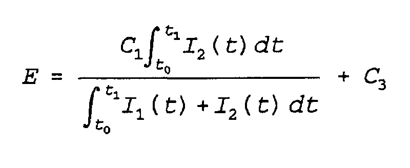
- the desired beam energy measurement (E) is described by the following equation: where C 1 and C 3 are calibration factors that relate this measurement of energy to the energy determination by the depth dose method (using an aluminum wedge and film) conventionally used.
- the conventional aluminum wedge and film method will provide a measured electron beam energy of say X1 MeV.
- the electronic circuit that solves Equation (2) will give an output of say Y1 volts for the same electron beam.
- a second measurement with an electron beam of a different energy using the wedge and film method will give a second energy of X2 MeV and the electronic circuit will give an output of Y2 MeV. From these two calibration points, the calibration factors C 1 and C 3 are calculated.
- C 1 is the sensitivity of the electronic measurement, i.e., MeV/volts
- C 3 is the threshold factor.
- C 3 is determined by the thickness of segment 1 and represents the threshold energy of electrons that will just penetrate segment 1 .
- C 3 is equal to about 7.5 MeV. Equation (2) is solved by electronically integrating the variables in the denominator for a time interval t 0 to t 1 that will yield a known constant, C 2 , i.e., a time interval t 0 to t 1 is calculated such that;
- the variable in the numerator is simultaneously integrated for exactly the same time interval.
- the energy, E is then electronically calculated by the following equation:
- Electron beam accelerators depending on the technology used to accelerate the beam, can produce a current that is continuous, i.e., dc current, or pulsed. If the accelerator produces pulses of beam current, the average current is determined by the pulse duration, the pulse frequency and the current during the pulse. To make an independent measurement of beam current and energy, the measurement should be carried out without using the timing circuit that is used to generate the accelerator pulse or else a failure of the timing circuit could give a correlated false measurement. Moreover, the integration of current is a good mimic of the way product accumulates dose. It is important that the integration of the numerator and denominator of equation (2) occur for a coincident time period. The electron beam from the accelerator is scanned across the beam stop and for a pulsed accelerator many of the pulses will impinge on two segments at the same time.
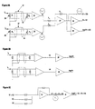
- FIG. 2A A circuit to develop voltages proportional to the charges deposited in segments 1 and 2 of beam stop 8 is shown in Figure 2A.
- Current I 1 from beam stop segment 1 flows through resistors 20 and 22 and shielded twisted pair cable 21 to generate a voltage V1 at the output of buffer amplifier 24.
- current I 2 from the lower segment 2 flows through resistors 26 and 28 and shielded twisted pair cable 27 to generate a voltage V2 at the output of buffer amplifier 30.
- V1 and V2 are summed by operational amplifier circuit 32 to produce -(V1 + V2) and then inverted by amplifier 34 to produce (V1 + V2).
- Amplifier 36 is a second order low pass filter that filters the ripple from each accelerator pulse and provides the average of (V1 + V2) that is proportional to the current from segments 1 and 2.
- the signals -(V1 + V2) and (V1 + V2) are used in the time base circuit shown in Figure 3A.
- a circuit to develop voltages proportional to the charges deposited in segments 3 and 4 of beam stop 8 is shown in Figure 2B.
- the operation of the circuit is similar to that of Figure 2A.
- Amplifiers 38 and 39 are second order low pass filters and provide the average of V3 and V4 that are proportional to the average of the current from segments 3 and 4 respectively.
- a circuit to develop voltages proportional to the sum of the charges deposited in segments 1 , 2 , 3 and 4 of beam stop 8 is shown in Figure 2C.
- Voltages (V1 + V2), V3 and V4 derived from the circuits of Figures 2A and 2B are summed in operational amplifier 40 and passed through second order low pass filter 41 to provide the average of (V1 + V2 + V3 + V4).
- the time base circuit of Figure 3A calculates the time t 0 to t 1 that yields the integral of V1 + V2 to be 2VC.
- the signal -(V1 + V2) is integrated by operational amplifier circuit 44.
- the charge accumulates (integrates) on capacitor 46 until a voltage VC is reached.
- This causes the output of comparator 48 to provide a logic true signal at its output.
- This causes the logic state of the bistable NORcircuit 50 to change which opens switch 42 and closes switch 52 .
- the signal V1 + V2 is applied to integrator circuit 44 which causes charge to be removed from capacitor 46.
- the output signal from amplifier 44 is a continuous triangular waveform such as that shown in Figure 3B.
- the output waveform of amplifier 44 is also triangular, but with a fine structure that is similar to stair steps.
- the peak to peak amplitude of the triangular waveform is a constant amplitude, 2VC, and the time that each of the logic signals A and B is true (t 1 -t 0 ) is proportional to V1 + V2.
- VC is a positive voltage applied to comparator 48.
- the inverted voltage -VC is applied to comparator 49 .
- the voltage VC is selected to permit amplifier 44 to integrate over a dynamic range that is as wide as possible. If amplifier 44 is designed to operate with +/- 15V power supplies, then typically good performance is achieved for a dynamic range of +/- 10V. For this situation, VC is selected to be +10V and then inverted to provide -VC of -10V.
- Figure 4A shows a circuit that solves equation (4) to give the energy of the electron beam using the time interval t 0 to t 1 from the time base circuit of Figure 3A.
- Figure 4B shows the sample and reset control for the energy integrator circuit of Figure 4A.
- the circuit generates pulses, SAMPLE56 and SAMPLE66 for sampling the output of operational integrating amplifiers 56 and 66 respectively, and reset pulses RESET56 and RESET66 respectively, for resetting to zero operational integrating amplifiers 56 and 66 respectively.
- the outputs of the circuits shown in Figures 2A, 2B and 2C permit beam parameters measurement.
- the average of signals I 1 + I 2 , I 3 and I 4 are used to calculate the scanned beam parameters.
- the average of I 1 +I 2 +I 3 +I 4 is used for the graphical display of scan-magnet current versus beam stop current.
- the electron beam scan width and scan offset measurements can be determined by a set of procedures and calculations based on the average current measured from segments.
- the equations for the measurements are given below.
- the equations have been derived by assuming that the beam spot has a uniform current density.
- the beam spot from an accelerator does not have a uniform current density and often shows a gaussian distribution. However, the assumption of uniform density is useful and valid when the product that is irradiated moves through the scanned beam.
- the movement through the beam integrates the beam current in the direction of motion and the current distribution is inconsequential. When the current is collected on beam stop segments that are longer than the beam spot diameter, the current is similarly integrated in the direction of motion.
- the beam's spot diameter must be determined first.
- the current from beam stop segments 1 and 2 are added together electronically to produce the same current as though the two segments were physically connected.
- the calibration constant of the drive magnet must be calculated.
- PRF Pulse Repetition Frequency
- a dc current is applied to scan magnet 14 to centre the beam on the boundary between segments 1 and 3 as shown in Figure 5A. The beam is centered on the boundary when I 3 is equal to I 1 + I 2 . The current through the scan magnet when the beam is centered is then recorded as I a .
- the measurement is repeated with the beam centered on the boundary between segments 1 and 4 to give a second current through the scan magnet, I b .
- the spot diameter is defined as the diameter that will provide 95% of the total current in the spot. This measurement is illustrated in Figure 5B.
- the accelerator is operated at a low PRF with the scanner stopped.
- the scan width measurement is shown in Figure 5C.
- the current flow from each segment is proportional to the area of the beam on the segment divided by the total area of the beam on the beam stop.
- Figure 5D illustrates the case where the scan width is less than the width of the centre beam stop segment.
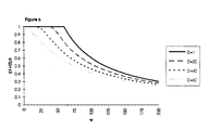
- Figure 6 is a graphical representation of the results of Equations 14 and 19 as a function of scan width with the centre segment width (b) set to 60.96 cm (24 inches) and spot diameter set to 1, 20, 40, and 60 cm.
- the same variables as shown in Figure 6 can be plotted for any accelerator and the spot diameter estimated by fitting a curve given by equation (2) to the data from the accelerator.
- the scan width can then be obtained from the centre beam stop segment current.
- Another parameter of the scanned beam which can be measured by the present invention is the offset from the centre line of the beam stop.
- the beam parameters derived from the beam stop will only be valid when there is no product being processed between the accelerator output and the beam stop. This occurs because product will absorb some or all of the incident electron beam and therefore only a residual of the electron beam is incident on the beam stop.
- the present invention can be used to provide a scan uniformity graphical display during processing to provide an indication of the current being absorbed by the product and assurance that product is moving through the beam.
- the scan uniformity can be obtained by displaying, in graphical form, the instantaneous electron beam current collected by the beam stop versus scan magnet current.
- FIG. 7 A plot showing a typical set of curves of instantaneous current versus scan magnet current is shown in Figure 7.
- the top curve indicated by the numeral 80 represents no tray or product between the accelerator and beam stop.
- the current collected by the beam stop is constant for all values of scan magnet current.
- the middle curve indicated by the numeral 82 is typical for an empty tray passing through the beam. The tray is about 25% stopping of the beam current and therefore the collected current is about 75% of nominal. When the scan magnet deflects the beam past the edges of the tray, the current increases to 100%.
- the bottom curve indicated by the numeral 86 is typical for a tray loaded with product where the product plus the tray are fully stopping. The product is narrower than the tray and therefore three values of current are collected by the beam stop: full current when the deflection is past the edge of the tray, 75% when the beam hits the tray but not product, and no current when the beam hits the product.
- the measurements that can be made with the method and apparatus of the present invention present a minimum disruption in the production schedule for the accelerator.
- the invention can also be used to maintain long term reliable calibration of the accelerator. While the invention has been described in association with an electron beam accelerator, those skilled in the art will understand that the invention is applicable to other charged particle beam applications. Moreover, while certain equations and circuits to implement said equations have been described, those skilled in the art will understand that other data and signal processing means can be used.
Landscapes
- Engineering & Computer Science (AREA)
- Physics & Mathematics (AREA)
- Plasma & Fusion (AREA)
- Spectroscopy & Molecular Physics (AREA)
- Ceramic Engineering (AREA)
- Metallurgy (AREA)
- General Engineering & Computer Science (AREA)
- High Energy & Nuclear Physics (AREA)
- Measurement Of Radiation (AREA)
- Analysing Materials By The Use Of Radiation (AREA)
- Tests Of Electronic Circuits (AREA)
Claims (12)
- Vorrichtung zum Bestimmen von Strahlparametern eines Elektronenstrahls mit:dadurch gekennzeichnet, dasseinem ersten strahlabsorbierenden Segment (1), das im Strahlengang angeordnet und dazu wirksam ist, einen Teil der darauf auftreffenden Elektronen zu absorbieren und den verbleibenden Teil der Elektronen den Durchgang zu erlauben,einem zweiten strahlabsorbierenden Segment (2), das hinter dem ersten absorbierenden Segment (1) angeordnet und dazu wirksam ist, Elektronen, die durch das erste absorbierende Segment hindurchtreten, zu absorbieren,einer Einrichtung (20-24, 26-30) zum Erfassen einer Eigenschaft der auf die ersten und zweiten strahlabsorbierenden Segmente (1, 2) auftreffenden Elektronen und zum Entwickeln von dementsprechenden elektrischen Signalen (V1, V2), undeiner Prozessoreinrichtung zum Umwandeln der elektrischen Signale (V1, V2) in ein Maß für die Strahlenergie,das zweite strahlabsorbierende Segment (2) dazu wirksam ist, den verbleibenden Teil der Elektronen, die durch das erste absorbierende Segment (1) hindurchtreten, zu absorbieren,die Einrichtung (20-24, 26-30) zum Erfassen der Eigenschaft der Elektronen dazu ausgestaltet ist, den Betrag an elektrischer Ladung, die durch den Strahl jeweils in dem ersten und dem zweiten strahlabsorbierenden Segment deponiert wird, zu erfassen und entsprechende elektrische Signale zu entwickeln, unddie Prozessoreinrichtung dazu ausgestaltet ist, die elektrischen Signale (V1, V2) in das Maß für die Strahlenergie auf Grundlage des relativen Betrags der in dem ersten und dem zweiten absorbierenden Segmenten (1, 2) deponierten Ladung umzuwandeln.
- Vorrichtung nach Anspruch 1, wobei die ersten und zweiten strahlabsorbierenden Segmente (1, 2) eine elektrisch leitfähige Struktur (6) mit internen Kanälen (7) zum Anschluss einer Kühlwasserquelle aufweisen.
- Vorrichtung nach Anspruch 2, wobei das Kühlwasser deionisiert wird und die Verbindung der Kühlwasserquelle elektrisch nicht leitfähig ist.
- Vorrichtung nach Anspruch 1, 2 oder 3, wobei das erste Segment (1) dazu wirksam ist, etwa 70 % der darauf auftreffenden geladenen Teilchen zu absorbieren.
- Vorrichtung nach einem der vorhergehenden Ansprüche, wobei die Prozessoreinrichtung die Stromsignale der ersten und zweiten absorbierenden Segmente in einen Wert E gemäß der folgenden Gleichung:umwandelt, wobei C1 und C3 Kalibrationsfaktoren sind, I1 der Strom von dem ersten absorbierenden Segment (1), I2 der Strom von dem zweiten absorbierenden Segment (2), und t0 bis t1 das Zeitintervall ist, das den Nenner gleich einer bekannten Konstanten C2 macht.
- Vorrichtung nach einem der vorhergehenden Ansprüche mit dritten und vierten absorbierenden Segmenten (3, 4), die zu beiden Seiten des ersten absorbierenden Segments (1) angeordnet sind und dazu wirksam sind, alle darauf auftreffenden Elektronen zu absorbieren, einer Einrichtung (FIG. 2B) zum Erfassen des Betrags der durch den Strahl jeweils in dem dritten und dem vierten strahlabsorbierenden Segment (3, 4) deponierten elektrischen Ladung und zum Entwickeln von dazu proportionalen elektrischen Signalen (V3, V4), wobei die Prozessoreinrichtung weiter dazu wirksam ist, die elektrischen Signale in ein Maß für den auf das erste absorbierende Segment auftreffenden Strahlstrom auf Grundlage der in den ersten und zweiten absorbierenden Segmenten deponierten Ladungsbeträge umzuwandeln, und für den auf die dritten und vierten absorbierenden Segmente auftreffenden Strahlstrom auf Grundlage der in den dritten und vierten absorbierenden Segmenten deponierten Ladungsbeträge umzuwandeln.
- Verfahren zum Bestimmen von Strahlparametern eines Elektronenstrahls, bei dem:dadurch gekennzeichnet, dassein erstes strahlabsorbierendes Segment im Strahlengang bereitgestellt wird, dass dazu wirksam ist, einen Teil der darauf auftreffenden Elektronen zu absorbieren und den verbleibenden Teil der Elektronen durchtreten zu lassen,ein zweites strahlabsorbierendes Segment (2) hinter dem ersten absorbierenden Segment (1) bereitgestellt wird, das dazu wirksam ist, Elektronen, die durch das erste absorbierende Segment hindurchtreten, zu absorbieren,eine Eigenschaft der auf die ersten und zweiten strahlabsorbierenden Segmente (1, 2) auftreffenden Elektronen erfasst und entsprechende elektrische Signale entwickelt werden, unddie elektrischen Signale in ein Maß für die Strahlenergie umgewandelt werden,das zweite strahlabsorbierende Segment (2) dazu wirksam ist, den verbleibenden Teil der Elektronen, die durch das erste absorbierende Segment (1) hindurchtreten, zu absorbieren,die erfasste Eigenschaft jeweils der Ladungsbetrag ist, der durch den Strahl in dem ersten und dem zweiten strahlabsorbierenden Segment deponiert wird, und die entwickelten elektrischen Signale (V1, V2) proportional dazu sind, undwobei das Maß für die Strahlenergie auf dem relativen Betrag der in dem ersten und dem zweiten absorbierenden Segmenten (1, 2) deponierten Ladung basiert.
- Verfahren nach Anspruch 7, wobei die strahlabsorbierenden Segmente (1, 2) jeweils elektrisch leitfähige Strukturen (6) mit internen Kanälen (7) aufweisen, wobei die Segmente gekühlt werden, indem Kühlwasser durch Kanäle (7) geleitet wird.
- Verfahren nach Anspruch 8, bei dem das Kühlwasser deionisiert wird und die Kühlwasserquelle von den Segmenten (1, 2) elektrisch isoliert ist.
- Verfahren nach Anspruch 7, 8 oder 9, wobei das erste Segment (1) dazu wirksam ist, etwa 70 % der darauf auftreffenden Elektronen zu absorbieren.
- Verfahren nach einem der Ansprüche 7 bis 10, wobei der Schritt des Umwandelns der Stromsignale des ersten und des zweiten absorbierenden Segments (1, 2) in einen Wert E gemäß der folgenden Gleichungvorgenommen wird, wobei C1 und C3 Kalibrationsfaktoren sind, I1 der Strom aus dem ersten absorbierenden Segment (1), I2 der Strom aus dem zweiten absorbierenden Segment (2), und t0 bis t1 das Zeitintervall ist, das den Nenner gleich einer bekannten Konstanten C2 macht.

- Verfahren nach einem der Ansprüche 7 bis 11, bei dem weiter dritte und vierte absorbierende Segmente (3, 4) auf beiden Seiten des ersten absorbierenden Segments (1) bereitgestellt werden, die dazu wirksam sind, alle darauf auftreffenden Elektronen zu absorbieren, bei dem der Betrag der durch den Strahl in jedem der dritten und vierten strahlabsorbierenden Segmente (3, 4) deponierten Ladung erfasst und dazu proportionale elektrische Signale (V3, V4) entwickelt werden, und bei dem die elektrischen Signale (V1, V2, V3, V4) in ein Maß für den auf das erste absorbierende Segment (1) auftreffenden Strahlstrom auf Grundlage der in dem ersten und zweiten absorbierenden Segment (1, 2) deponierten Ladung umgewandelt wird, und für den auf jedes der dritten und vierten absorbierenden Segmente (3, 4) auftreffenden Strahlstrom auf Grundlage der in den dritten und vierten absorbierenden Segmenten (3, 4) deponierten Ladung umgewandelt wird.
Applications Claiming Priority (3)
| Application Number | Priority Date | Filing Date | Title |
|---|---|---|---|
| US08/392,512 US5714875A (en) | 1995-02-23 | 1995-02-23 | Electron beam stop analyzer |
| US392512 | 1995-02-23 | ||
| PCT/CA1996/000072 WO1996026454A1 (en) | 1995-02-23 | 1996-02-07 | Electron beam stop analyzer |
Publications (2)
| Publication Number | Publication Date |
|---|---|
| EP0811172A1 EP0811172A1 (de) | 1997-12-10 |
| EP0811172B1 true EP0811172B1 (de) | 2001-11-07 |
Family
ID=23550893
Family Applications (1)
| Application Number | Title | Priority Date | Filing Date |
|---|---|---|---|
| EP96901203A Expired - Lifetime EP0811172B1 (de) | 1995-02-23 | 1996-02-07 | Analysierender elektronstrahl-stopper |
Country Status (9)
| Country | Link |
|---|---|
| US (1) | US5714875A (de) |
| EP (1) | EP0811172B1 (de) |
| JP (1) | JPH11500531A (de) |
| AT (1) | ATE208509T1 (de) |
| AU (1) | AU4532896A (de) |
| CA (1) | CA2196411C (de) |
| DE (1) | DE69616763D1 (de) |
| DK (1) | DK0811172T3 (de) |
| WO (1) | WO1996026454A1 (de) |
Families Citing this family (11)
| Publication number | Priority date | Publication date | Assignee | Title |
|---|---|---|---|---|
| JP2002509361A (ja) * | 1997-12-18 | 2002-03-26 | マイクロン テクノロジー, インク. | 半導体製造方法及び電界効果トランジスタ |
| US6919570B2 (en) * | 2002-12-19 | 2005-07-19 | Advanced Electron Beams, Inc. | Electron beam sensor |
| JP4914568B2 (ja) * | 2004-11-11 | 2012-04-11 | オリンパス株式会社 | 受光装置 |
| US8314386B2 (en) | 2010-03-26 | 2012-11-20 | Uchicago Argonne, Llc | High collection efficiency X-ray spectrometer system with integrated electron beam stop, electron detector and X-ray detector for use on electron-optical beam lines and microscopes |
| CA2713972A1 (en) * | 2010-07-27 | 2012-01-27 | Mevex Corporation | Power concentrator for electron and/or x-ray beams |
| US10535441B1 (en) | 2010-07-27 | 2020-01-14 | Mevex Corporation | Method of irradiating a target |
| CN103377864B (zh) * | 2012-04-28 | 2015-11-18 | 中国科学院电子学研究所 | 用于真空电子器件的强流电子注能散测量系统及测量方法 |
| CN110312358A (zh) * | 2018-03-20 | 2019-10-08 | 先进肿瘤治疗公开有限公司 | 改善线性加速器的安全性 |
| US10748740B2 (en) * | 2018-08-21 | 2020-08-18 | Fei Company | X-ray and particle shield for improved vacuum conductivity |
| CN111538065A (zh) * | 2020-06-15 | 2020-08-14 | 上海高鹰科技有限公司 | 一种辐照加速器电子束流的在线扫描参数检测系统 |
| CN114200505A (zh) * | 2021-12-27 | 2022-03-18 | 中广核达胜加速器技术有限公司 | 电子加速器束流强度测量装置 |
Family Cites Families (14)
| Publication number | Priority date | Publication date | Assignee | Title |
|---|---|---|---|---|
| US3733546A (en) * | 1971-07-21 | 1973-05-15 | Atomic Energy Commission | Beam current position, intensity and profile monitoring by resistive detection of beam image wall currents |
| DE2824308A1 (de) * | 1978-06-02 | 1979-12-13 | Siemens Ag | Verfahren zum einpraegen einer spannung mit einem elektronenstrahl |
| DE2831602A1 (de) * | 1978-07-19 | 1980-02-07 | Leybold Heraeus Gmbh & Co Kg | Vorrichtung zur erfassung von strahlparametern eines periodisch ueber eine zielflaeche gefuehrten, fokussierten ladungstraegerstrahls und messverfahren unter verwendung der vorrichtung |
| FR2441182A1 (fr) * | 1978-11-07 | 1980-06-06 | Thomson Csf | Dispositif de visualisation de la repartition de la densite du courant au sein d'un faisceau de particules chargees |
| JPS5618422A (en) * | 1979-07-23 | 1981-02-21 | Hitachi Ltd | Measuring method for diameter of electron beam |
| SU869473A1 (ru) * | 1980-05-13 | 1985-06-15 | Научно-Исследовательский Институт Электронной Интроскопии При Томском Ордена Октябрьской Революции И Ордена Трудового Красного Знамени Политехническом Институте Им.С.М.Кирова | Способ измерени энергии электронов в пучке |
| GB2098793A (en) * | 1981-05-18 | 1982-11-24 | Varian Associates | Method of and apparatus for deflecting an ion beam of an ion implantater onto an ion absorbing target |
| SU1066050A1 (ru) * | 1982-09-06 | 1984-01-07 | Московский Государственный Научно-Исследовательский Рентгено-Радиологический Институт | Способ регулировани энергии в установке дл облучени объектов жестким тормозным излучением |
| US4629975A (en) * | 1984-06-19 | 1986-12-16 | The United States Of America As Represented By The Secretary Of The Navy | Coaxial probe for measuring the current density profile of intense electron beams |
| US4724324A (en) * | 1986-11-24 | 1988-02-09 | Varian Associates, Inc. | Method and apparatus for ion beam centroid location |
| US4992742A (en) * | 1988-12-22 | 1991-02-12 | Mitsubishi Denki Kabushiki Kaisha | Charged-particle distribution measuring apparatus |
| US5138256A (en) * | 1991-04-23 | 1992-08-11 | International Business Machines Corp. | Method and apparatus for determining the thickness of an interfacial polysilicon/silicon oxide film |
| RU2009526C1 (ru) * | 1991-07-15 | 1994-03-15 | Харьковский физико-технический институт | Устройство для диагностики параметров потока электронов |
| US5198676A (en) * | 1991-09-27 | 1993-03-30 | Eaton Corporation | Ion beam profiling method and apparatus |
-
1995
- 1995-02-23 US US08/392,512 patent/US5714875A/en not_active Expired - Fee Related
-
1996
- 1996-02-07 AU AU45328/96A patent/AU4532896A/en not_active Abandoned
- 1996-02-07 CA CA002196411A patent/CA2196411C/en not_active Expired - Fee Related
- 1996-02-07 DK DK96901203T patent/DK0811172T3/da active
- 1996-02-07 AT AT96901203T patent/ATE208509T1/de not_active IP Right Cessation
- 1996-02-07 DE DE69616763T patent/DE69616763D1/de not_active Expired - Lifetime
- 1996-02-07 WO PCT/CA1996/000072 patent/WO1996026454A1/en not_active Ceased
- 1996-02-07 EP EP96901203A patent/EP0811172B1/de not_active Expired - Lifetime
- 1996-02-07 JP JP8525256A patent/JPH11500531A/ja active Pending
Also Published As
| Publication number | Publication date |
|---|---|
| DK0811172T3 (da) | 2002-01-21 |
| US5714875A (en) | 1998-02-03 |
| AU4532896A (en) | 1996-09-11 |
| ATE208509T1 (de) | 2001-11-15 |
| CA2196411C (en) | 1999-11-30 |
| JPH11500531A (ja) | 1999-01-12 |
| WO1996026454A1 (en) | 1996-08-29 |
| EP0811172A1 (de) | 1997-12-10 |
| CA2196411A1 (en) | 1996-08-29 |
| DE69616763D1 (de) | 2001-12-13 |
Similar Documents
| Publication | Publication Date | Title |
|---|---|---|
| EP0811172B1 (de) | Analysierender elektronstrahl-stopper | |
| US3953732A (en) | Dynamic mass spectrometer | |
| Spanggaard | Delay wire chambers-a users guide | |
| US4288692A (en) | Beam current normalization in an X-ray microanalysis instrument | |
| Goodman et al. | A facility for studying neutron energy spectra at intermediate energies | |
| Crawford et al. | A precision luminosity monitor for use at electron-positron storage rings | |
| Carter et al. | The OPAL vertex drift chamber | |
| Pasour et al. | Nonperturbing electron beam probe to diagnose charged‐particle beams | |
| US5880477A (en) | Method of real time control of ionizing radiation dose rate and device for using same | |
| Saito et al. | Study of low-frequency turbulence in the WT-1 tokamak plasma by CW FIR laser scattering | |
| Bakhmetjev et al. | Research into the advanced experimental methods for precision ion stopping range measurements in matter | |
| Møller et al. | Measurement of the Barkas effect around the stopping-power maximum for light and heavy targets | |
| Armentrout et al. | E parallel B canted detector neutral‐particle spectrometer | |
| Ishii et al. | The energy component analyzer and spectrum analysis of end‐loss ions in a tandem mirror | |
| Fessenden | The Astron On‐Line Beam Energy Analyzer | |
| JPH063296A (ja) | オージェ電子分光装置 | |
| Chamberlain et al. | Proton-Proton Scattering Experiments at 170 and 260 Mev | |
| SU1109693A1 (ru) | Способ измерени энергетического спектра электронного пучка и устройство дл его осуществлени | |
| US20260118533A1 (en) | Technique for determining the smearing of the kinetic energy of a hadron beam | |
| Krick et al. | The 16O (3He, n) 18Ne double-stripping reaction | |
| Aulchenko et al. | One-and two-coordinate detectors in BINP | |
| Kugel et al. | Neutral beam species measurements using in situ Rutherford backscatter spectrometry | |
| Nedzelskiy et al. | Multichannel time-of-flight technique for plasma potential profile measurements by heavy ion beam diagnostic on the tokamak ISTTOK | |
| Pasour et al. | Ion probe for tightly bunched charged particle beams | |
| Wharton | Clean turbulent heating. Final report |
Legal Events
| Date | Code | Title | Description |
|---|---|---|---|
| PUAI | Public reference made under article 153(3) epc to a published international application that has entered the european phase |
Free format text: ORIGINAL CODE: 0009012 |
|
| 17P | Request for examination filed |
Effective date: 19970214 |
|
| AK | Designated contracting states |
Kind code of ref document: A1 Designated state(s): AT BE CH DE DK FR GB IT LI NL SE |
|
| 17Q | First examination report despatched |
Effective date: 19991021 |
|
| GRAG | Despatch of communication of intention to grant |
Free format text: ORIGINAL CODE: EPIDOS AGRA |
|
| GRAG | Despatch of communication of intention to grant |
Free format text: ORIGINAL CODE: EPIDOS AGRA |
|
| GRAH | Despatch of communication of intention to grant a patent |
Free format text: ORIGINAL CODE: EPIDOS IGRA |
|
| GRAH | Despatch of communication of intention to grant a patent |
Free format text: ORIGINAL CODE: EPIDOS IGRA |
|
| GRAA | (expected) grant |
Free format text: ORIGINAL CODE: 0009210 |
|
| AK | Designated contracting states |
Kind code of ref document: B1 Designated state(s): AT BE CH DE DK FR GB IT LI NL SE |
|
| PG25 | Lapsed in a contracting state [announced via postgrant information from national office to epo] |
Ref country code: NL Free format text: LAPSE BECAUSE OF FAILURE TO SUBMIT A TRANSLATION OF THE DESCRIPTION OR TO PAY THE FEE WITHIN THE PRESCRIBED TIME-LIMIT Effective date: 20011107 Ref country code: LI Free format text: LAPSE BECAUSE OF FAILURE TO SUBMIT A TRANSLATION OF THE DESCRIPTION OR TO PAY THE FEE WITHIN THE PRESCRIBED TIME-LIMIT Effective date: 20011107 Ref country code: IT Free format text: LAPSE BECAUSE OF FAILURE TO SUBMIT A TRANSLATION OF THE DESCRIPTION OR TO PAY THE FEE WITHIN THE PRE;WARNING: LAPSES OF ITALIAN PATENTS WITH EFFECTIVE DATE BEFORE 2007 MAY HAVE OCCURRED AT ANY TIME BEFORE 2007. THE CORRECT EFFECTIVE DATE MAY BE DIFFERENT FROM THE ONE RECORDED.SCRIBED TIME-LIMIT Effective date: 20011107 Ref country code: FR Free format text: LAPSE BECAUSE OF FAILURE TO SUBMIT A TRANSLATION OF THE DESCRIPTION OR TO PAY THE FEE WITHIN THE PRESCRIBED TIME-LIMIT Effective date: 20011107 Ref country code: CH Free format text: LAPSE BECAUSE OF FAILURE TO SUBMIT A TRANSLATION OF THE DESCRIPTION OR TO PAY THE FEE WITHIN THE PRESCRIBED TIME-LIMIT Effective date: 20011107 Ref country code: AT Free format text: LAPSE BECAUSE OF FAILURE TO SUBMIT A TRANSLATION OF THE DESCRIPTION OR TO PAY THE FEE WITHIN THE PRESCRIBED TIME-LIMIT Effective date: 20011107 |
|
| REF | Corresponds to: |
Ref document number: 208509 Country of ref document: AT Date of ref document: 20011115 Kind code of ref document: T |
|
| RAP2 | Party data changed (patent owner data changed or rights of a patent transferred) |
Owner name: IOTRON INDUSTRIES CANADA INC., |
|
| REG | Reference to a national code |
Ref country code: CH Ref legal event code: EP |
|
| REF | Corresponds to: |
Ref document number: 69616763 Country of ref document: DE Date of ref document: 20011213 |
|
| REG | Reference to a national code |
Ref country code: GB Ref legal event code: IF02 |
|
| NLT2 | Nl: modifications (of names), taken from the european patent patent bulletin |
Owner name: IOTRON INDUSTRIES CANADA INC., |
|
| REG | Reference to a national code |
Ref country code: DK Ref legal event code: T3 |
|
| PG25 | Lapsed in a contracting state [announced via postgrant information from national office to epo] |
Ref country code: SE Free format text: LAPSE BECAUSE OF FAILURE TO SUBMIT A TRANSLATION OF THE DESCRIPTION OR TO PAY THE FEE WITHIN THE PRESCRIBED TIME-LIMIT Effective date: 20020207 Ref country code: GB Free format text: LAPSE BECAUSE OF NON-PAYMENT OF DUE FEES Effective date: 20020207 |
|
| PG25 | Lapsed in a contracting state [announced via postgrant information from national office to epo] |
Ref country code: DE Free format text: LAPSE BECAUSE OF FAILURE TO SUBMIT A TRANSLATION OF THE DESCRIPTION OR TO PAY THE FEE WITHIN THE PRESCRIBED TIME-LIMIT Effective date: 20020208 |
|
| NLV1 | Nl: lapsed or annulled due to failure to fulfill the requirements of art. 29p and 29m of the patents act | ||
| REG | Reference to a national code |
Ref country code: CH Ref legal event code: PL |
|
| EN | Fr: translation not filed | ||
| PLBE | No opposition filed within time limit |
Free format text: ORIGINAL CODE: 0009261 |
|
| STAA | Information on the status of an ep patent application or granted ep patent |
Free format text: STATUS: NO OPPOSITION FILED WITHIN TIME LIMIT |
|
| GBPC | Gb: european patent ceased through non-payment of renewal fee |
Effective date: 20020207 |
|
| 26N | No opposition filed | ||
| PGFP | Annual fee paid to national office [announced via postgrant information from national office to epo] |
Ref country code: DK Payment date: 20040123 Year of fee payment: 9 |
|
| PGFP | Annual fee paid to national office [announced via postgrant information from national office to epo] |
Ref country code: BE Payment date: 20040323 Year of fee payment: 9 |
|
| PG25 | Lapsed in a contracting state [announced via postgrant information from national office to epo] |
Ref country code: DK Free format text: LAPSE BECAUSE OF NON-PAYMENT OF DUE FEES Effective date: 20050228 Ref country code: BE Free format text: LAPSE BECAUSE OF NON-PAYMENT OF DUE FEES Effective date: 20050228 |
|
| BERE | Be: lapsed |
Owner name: *IOTRON INDUSTRIES CANADA INC. Effective date: 20050228 |
|
| REG | Reference to a national code |
Ref country code: DK Ref legal event code: EBP |
|
| BERE | Be: lapsed |
Owner name: *IOTRON INDUSTRIES CANADA INC. Effective date: 20050228 |