EP0811181B1 - Verfahren und vorrichtung zum strukturieren einer photolithographischen schicht - Google Patents
Verfahren und vorrichtung zum strukturieren einer photolithographischen schichtInfo
- Publication number
- EP0811181B1 EP0811181B1 EP96914126A EP96914126A EP0811181B1 EP 0811181 B1 EP0811181 B1 EP 0811181B1 EP 96914126 A EP96914126 A EP 96914126A EP 96914126 A EP96914126 A EP 96914126A EP 0811181 B1 EP0811181 B1 EP 0811181B1
- Authority
- EP
- European Patent Office
- Prior art keywords
- pattern
- light
- light source
- region
- layer
- Prior art date
- Legal status (The legal status is an assumption and is not a legal conclusion. Google has not performed a legal analysis and makes no representation as to the accuracy of the status listed.)
- Expired - Lifetime
Links
Images


Classifications
-
- G—PHYSICS
- G03—PHOTOGRAPHY; CINEMATOGRAPHY; ANALOGOUS TECHNIQUES USING WAVES OTHER THAN OPTICAL WAVES; ELECTROGRAPHY; HOLOGRAPHY
- G03F—PHOTOMECHANICAL PRODUCTION OF TEXTURED OR PATTERNED SURFACES, e.g. FOR PRINTING, FOR PROCESSING OF SEMICONDUCTOR DEVICES; MATERIALS THEREFOR; ORIGINALS THEREFOR; APPARATUS SPECIALLY ADAPTED THEREFOR
- G03F7/00—Photomechanical, e.g. photolithographic, production of textured or patterned surfaces, e.g. printing surfaces; Materials therefor, e.g. comprising photoresists; Apparatus specially adapted therefor
- G03F7/70—Microphotolithographic exposure; Apparatus therefor
- G03F7/70425—Imaging strategies, e.g. for increasing throughput or resolution, printing product fields larger than the image field or compensating lithography- or non-lithography errors, e.g. proximity correction, mix-and-match, stitching or double patterning
- G03F7/70466—Multiple exposures, e.g. combination of fine and coarse exposures, double patterning or multiple exposures for printing a single feature
-
- G—PHYSICS
- G03—PHOTOGRAPHY; CINEMATOGRAPHY; ANALOGOUS TECHNIQUES USING WAVES OTHER THAN OPTICAL WAVES; ELECTROGRAPHY; HOLOGRAPHY
- G03F—PHOTOMECHANICAL PRODUCTION OF TEXTURED OR PATTERNED SURFACES, e.g. FOR PRINTING, FOR PROCESSING OF SEMICONDUCTOR DEVICES; MATERIALS THEREFOR; ORIGINALS THEREFOR; APPARATUS SPECIALLY ADAPTED THEREFOR
- G03F7/00—Photomechanical, e.g. photolithographic, production of textured or patterned surfaces, e.g. printing surfaces; Materials therefor, e.g. comprising photoresists; Apparatus specially adapted therefor
- G03F7/70—Microphotolithographic exposure; Apparatus therefor
- G03F7/70216—Mask projection systems
- G03F7/70283—Mask effects on the imaging process
- G03F7/70291—Addressable masks, e.g. spatial light modulators [SLMs], digital micro-mirror devices [DMDs] or liquid crystal display [LCD] patterning devices
Definitions
- the present invention relates to a method and a Device for structuring photolithographic layers, especially for microelectronics, microsystem technology, thin film technology, the production of flat Screens direct exposure of semiconductor wafers in semiconductor manufacturing and mask structuring and reticles for microlithographic applications.
- Exposure devices are already in the prior art for direct exposure of light-sensitive layers known.
- WO 93/09472 describes an exposure device which a light source and a pattern generator.
- the pattern generator has an optical streak system and one active, matrix-addressable area light modulator.
- this known exposure device comprises one movable positioning table on which a to be exposed Substrate can be determined.
- a pulsed light source is used there Laser used, the pulse duration is so short that with a continuous movement of the substrate Positioning table during exposure of a single image no image blurring impairing the image quality occur. That way are relative high writing speeds achievable.
- WO 91/17483 and WO 93/09469 describe similar exposure devices for direct exposure of photosensitive Layers where this exposure is also done by an area light modulator.
- the disadvantage of the exposure devices described above consists in the fact that the size of the picture elements (pixels) in particular by the width of the picture elements on the area light modulator and because of the image scale a structural increment is predetermined for a projection optical system is and cannot be reduced to any size.
- a structural increment is the smallest unit around which a structure enlarged or reduced on the substrate to be exposed can be.
- the structural increment can only expose devices in a technologically or technically limited framework by enlarging the image scale of the projection optics or by reducing the width of the picture elements be reduced on the area light modulator.
- Another disadvantage of these known devices represents the defect sensitivity of these devices. Due to the size of the area light modulators used are usually defects on the area light modulator cannot be excluded, i.e. a number of picture elements cannot be addressed or cannot be addressed completely.
- WO 93/09472 solves this problem in that all defects Image elements are determined and processed in such a way that they no longer reflect light.
- this known Device becomes a structure by overlapping each other Fields created so that it is ensured that everyone Part of the structure to be exposed at least once a functional image element is exposed. This overlap of two adjacent individual images the substrate leads to a reduction in the writing speed this known device by a further factor of two.
- the present invention has for its object a method and a device for structuring a photolithographic Create layer where a restriction the size of a structure increment due to the pixel width of the area light modulator and based on the image scale of the projection lens without interference the writing speed is canceled.
- the present invention is based on the finding that that it is due to the finite aperture of the optical imaging device on the edges of the structures for a decrease the light intensity comes, so that an edge to be imaged "washed out” appears.
- the contrast of the used resists which is a measure of the resist removal a change in light intensity, and that on the Resist incident light intensity can by variation the steepness of the intensity curve on the image to be imaged Structure edge the width of the resist structure created to be influenced.
- response intensity of the resist In the ideal case of a resist with infinitely high contrast there is a so-called response intensity of the resist.
- a structure edge is in this Fall through the intersection of the intensity curve with the Response intensity of the resist set.
- Fig. 1 is a first pattern 100 and a second pattern 102 shown.
- the first pattern 100 is on an area light modulator generated and exists in this embodiment from 3 x 5 addressed picture elements.
- the second Pattern 102 is also generated on an area light modulator and consists of 4 x 5 addressed picture elements.
- the second pattern 102 has a first area 102a of 3 ⁇ 5 addressed picture elements corresponding to an area 100a. Adjacent to the first area 102a of the second Pattern is a second area 102b with 1 x 5 addressed Arranged picture elements of the second pattern.
- 104 is the resulting exposed area represented on the layer to be structured. How clear can be seen results from an overlay of the first pattern 100 and the second pattern 102 is an exposed one Region 104, which has a first section 104a, which corresponds to the first pattern 100. Furthermore results a second section 104b that has a width that half the width of a picture element of the area light modulator corresponds.
- This second section is as follows based on the intensity profiles in the lower part of FIG. 1 explained in more detail.
- the first intensity curve represents the intensity of the Represents light due to the first or second pattern 100, 102 is reflected by the surface light modulator. It is clearly a sharp transition between picture elements of the Area light modulators that define the first or second pattern, and between picture elements of the area light modulator, that do not define any part of the pattern.
- the imaging optics a finite aperture. This leads to the fact that the originally sharp transition of light intensity after the Area light modulator "washed out".
- FIG. 1 shows the intensity curve of the light after it has passed through the imaging optics.
- I 1 denotes the light intensity that is required in order to expose the area to be exposed with all 3 ⁇ 5 addressed picture elements of the first pattern 100.
- I 2 denotes the light intensity which is required in order to expose the area to be exposed with all 4 ⁇ 5 addressed picture elements of the second pattern 102.
- the patterns 100, 102 are not exposed to the intensity, I 1 or I 2 , which is required to image the complete pattern, but lower intensities are used, which are below the above intensities.
- the corresponding intensities depend on the resist used.
- the exposed area 104 with its first and its second section 104a, 104b, the second section 104b has a width that is half that Width of a picture element of an area light modulator corresponds.
- FIG. 2 Another example is shown in FIG. In Fig. 2 the same reference numerals are used as in Fig. 1.
- the first pattern 100 is made there from two partial patterns 100a and the second pattern 102 accordingly has two partial patterns.
- the resulting one exposed area 104 also has two partial areas on.
- the plus sign indicates the overlay of the two patterns 100, 102 indicated, from which the exposed Area 104 gives what is indicated by the actual equal sign is shown.
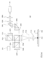
- the device according to the invention is in its entirety with provided with the reference number 300.
- the device 300 comprises two area light modulators 302a, 302b, which have a plurality of picture elements having. Via a controller 304 which is connected to the Area light modulators are connected to patterns This area light modulator 302 can be generated.
- a light source 306 which in this preferred embodiment can be a pulsed laser light source the light emerging from this is and transmission unit 308a-308e and via one Beam splitter cube 310 onto the surface light modulators 302a, 302b projected.
- the light reflected by the surface light modulators passes through and passes through the beam splitter cube 310 a so-called projection or imaging optics 312a, 312b, 312c and finally falls on one to be exposed Area 314 of a layer 316 to be structured.
- the layer to be structured is in this embodiment arranged on a movable positioning table 318.
- the beam splitter cube 310 is accordingly designed to split the beam coming from the light source 306 into two parts in order to direct it to the respective area light modulators.
- the beam splitter cube divides 310 that of the light source 306, which is also a pulsed one here Laser light source can be coming light in two equal intensity Partial beams.
- the invention includes follows the steps below:
- a first pattern is created on the first Area light modulator 302a generated by a predetermined Number of addressed picture elements defined is.
- a second step is carried out at the same time Generated patterns on the second area light modulator 302b, which has a first range of addressed picture elements, that matches the first pattern, immediately adjacent to the first area a second area of addressed picture elements. Subsequently the first and the second pattern will be on the one to be exposed Area 314 of the layer 316 to be structured is imaged.
- the second area of the second pattern can in this embodiment perpendicular to the direction of expansion of the first Area of the second pattern an addressed picture element include.
- Area light modulator 302a has a first pattern with a width of i addressed picture elements and on the second area light modulator a second pattern with a width of i + 1 addressed picture elements generated.
- this is the coherent overlay of the individual partial images responsible for the creation of the forest.
- the imaging principle is based on the fact that the and in-phase overlay of the light excitations of the individual patterns on the area light modulator a virtual pattern is generated which is imaged on the substrate becomes.
- This pattern also shows in the border areas intensity modulation for phase modulation which causes the structure edge to shift (see Fig. 1). This is programmed through those described above Area light modulators with different programmed patterns.
- the result is the overall structure due to the incoherent overlay of the individual partial images, as described with reference to FIG. 1 has been.
- the device according to the invention is in its entirety with designated by reference numeral 400.
- the device 400 differs from that in FIG. 3 device shown in that instead of the two Area light modulators four area light modulators 302a - 302d can be used. Accordingly, three beam splitter cubes 310a - 310c used to block the light from the Light source 306 on the individual area light modulators 302a - 302d to be distributed and imaged on the image to be exposed Combine area 314 again.
- the surface light modulators 302a - 302d have, for example a width of the picture elements of 20 ⁇ m, and the magnification of the imaging optics is 312a-312c 100: 1.
- the width of a structural increment is thus 0.2 ⁇ m.
- a factor 4 reduction to the required 0.05 ⁇ m which means structure widths of 0.50 ⁇ m, 0.55 ⁇ m, 0.60 ⁇ m, etc. can be exposed.
- N 4 surface light modulators
- All surface light modulators are in a first operating mode (two or more) identical, but will be different programs or have different patterns.
- This mode of operation is used to determine the structural increment the image below that by the pixel dimensions on the Area light modulator multiplied by the magnification reduce the size of the imaging optics, as already described above.
- All surface light modulators are in a second operating mode identical and programmed the same or have the same Pattern on.
- This mode is used to measure the energy of the light source completely for illuminating area light modulators to use, so that the exposure of the substrate with a lower light energy by a factor of two - compared to conventional devices.
- the surface light modulators are in a third operating mode not identical.
- This operating mode is used when for certain Applications of using area light modulators with a firmly embossed pattern (passive elements) makes sense is, e.g. for creating patterns with a high degree Structure repetitions. Individuals can then choose Area light modulators (either active matrix-addressable or the passive elements) are not illuminated by shutter and therefore do not contribute to the image.
Landscapes
- Physics & Mathematics (AREA)
- General Physics & Mathematics (AREA)
- Exposure And Positioning Against Photoresist Photosensitive Materials (AREA)
Description
Claims (15)
- Verfahren zum Strukturieren einer photolithographischen Schicht, mit folgenden Schritten:gekennzeichnet durcha) Erzeugen eines ersten Musters (100) auf einem ersten Flächenlichtmodulator (302a), wobei der erste Flächenlichtmodulator (302a) eine Mehrzahl von Bildelementen aufweist, wobei das erste Muster (100) durch eine vorbestimmte Anzahl von adressierten Bildelementen festgelegt ist; undb) Abbilden des ersten Musters (100) auf einem zu belichtenden Bereich (314) der zu strukturierenden Schicht (316) ;wobei das erste und das zweite Muster (100, 102) gleichzeitig auf den zu belichtenden Bereich (314) der zu strukturierenden Schicht (316) abgebildet werden.c) Erzeugen eines zweiten Musters (102) auf einem zweiten Flächenlichtmodulator (302b), wobei der zweite Flächenlichtmodulator (302b) eine Mehrzahl von Bildelementen aufweist, wobei das zweite Muster (102) einen ersten Bereich (102a) von adressierten Bildelementen, der mit dem ersten Muster oder einem Teil daraus (100) übereinstimmt, und unmittelbar benachbart zu diesem einen zweiten Bereich (102b) von adressierten Bildelementen aufweist; undd) Abbilden des zweiten Musters (102) auf dem zu belichtenden Bereich (314) der zu strukturierenden Schicht (316);
- Verfahren nach Anspruch 1, dadurch gekennzeichnet,daß der zweite Bereich (102b) des zweiten Musters senkrecht zur Ausdehnungsrichtung des ersten Bereichs (102a) des zweiten Musters ein adressiertes Bildelement umfaßt.
- Verfahren nach Anspruch 1 oder 2, dadurch gekennzeichnet,daß der erste und der zweite Flächenlichtmodulator (302a, 302b) von einer Lichtquelle (306) beleuchtet werden.
- Verfahren nach Anspruch 3, dadurch gekennzeichnet,daß die Differenz der Lichtwege von der Lichtquelle (306) über den ersten und den zweiten Flächenlichtmodulator (302a, 302b) zu der zu strukturierenden Schicht (316) kleiner ist als die Kohärenzlänge des Lichtes der Lichtquelle (306).
- Verfahren nach Anspruch 1 oder 2, dadurch gekennzeichnet,daß der erste und der zweite Flächenlichtmodulator (302a, 302b) von einer ersten und einer zweiten Lichtquelle belichtet werden, wobei die erste und die zweite Lichtquelle miteinander interferieren.
- Verfahren nach Anspruch 5, dadurch gekennzeichnet,daß die Differenz der Lichtwege von der ersten Lichtquelle über den ersten Flächenlichtmodulator (302a) und von der zweiten Lichtquelle über den zweiten Flächenlichtmodulator (302b) zu der zu strukturierenden Schicht (316) kleiner ist als die Kohärenzlänge des Lichtes der Lichtquelle (306).
- Vorrichtung zum Strukturieren einer photolithographischen Schicht, mitgekennzeichnet durcheinem ersten Flächenlichtmodulator (302a) mit einer Mehrzahl von Bildelementen zum Erzeugen eines ersten Musters (100), das durch eine vorbestimmte Anzahl von adressierten Bildelementen festgelegt ist; undeiner Abbildungseinrichtung (312a - 312c), die das erste Muster auf einen zu belichtenden Bereich (314) der zu strukturierenden Schicht (316) abbildet;einen zweiten Flächenlichtmodulator (302b) mit einer Mehrzahl von Bildelementen zum Erzeugen eines zweiten Musters (102), das einen ersten Bereich von adressierten Bildelementen, der mit dem ersten Muster oder einem Teil daraus übereinstimmt, und unmittelbar benachbart zu diesem einen zweiten Bereich von adressierten Bildelementen aufweist; undwobei die Abbildungseinrichtung (312a - 312c) das zweite Muster auf den zu belichtenden Bereich (314) der zu strukturierenden Schicht (316) abbildet;wobei die Abbildungseinrichtung (312a - 312c) das erste und das zweite Muster (100, 102) gleichzeitig auf den zu belichtenden Bereich (314) der zu strukturierenden Schicht (316) abbildet.
- Vorrichtung nach Anspruch 7, dadurch gekennzeichnet,daß der zweite Bereich (102b) des zweiten Musters senkrecht zur Ausdehnunqsrichtunq des ersten Bereichs (102a) des zweiten Musters ein adressiertes Bildelement aufweist.
- Vorrichtung nach Anspruch 7 oder 8, gekennzeichnet durcheine erste Lichtquelle, die dem ersten Flächenlichtmodulator zugeordnet ist; undeine zweite Lichtquelle, die dem zweiten Flächenlichtmodulator zugeordnet ist, deren Licht mit dem Licht der ersten Lichtquelle interferieren kann.
- Vorrichtung nach Anspruch 9, dadurch gekennzeichnet,daß die Differenz der Lichtwege von der ersten Lichtquelle über den ersten Flächenlichtmodulator (302a) und von der zweiten Lichtquelle über den zweiten Flächenlichtmodulator (302b) zu der zu strukturierenden Schicht (316) kleiner ist als die Kohärenzlänge des Lichtes der Lichtquelle (306).
- Vorrichtung nach Anspruch 7 oder 8, gekennzeichnet durcheine Lichtquelle (306); undeine Strahlteilereinrichtung (310), die den Lichtstrahl von der Lichtquelle (306) auf den ersten und auf den zweiten Flächenlichtmodulator (302a, 302b) richtet.
- Vorrichtung nach Anspruch 11, dadurch gekennzeichnet,daß die Differenz der Lichtwege von der Lichtquelle (306) über den ersten und den zweiten Flächenlichtmodulator (302a, 302b) zu der zu strukturierenden Schicht (316) kleiner ist als die Kohärenzlänge des Lichtes der Lichtquelle (306).
- Vorrichtung nach Anspruch 11 oder 12, dadurch gekennzeichnet,daß die Strahlteilereinrichtung (310) den Lichtstrahl von der Lichtquelle (306) in zwei intensitätsgleiche Strahlen aufteilt.
- Vorrichtung nach einem der Ansprüche 9 bis 13, dadurch gekennzeichnet,daß die Lichtquelle (306) eine gepulste Laserlichtquelle ist.
- Vorrichtung nach einem der Ansprüche 7 bis 14, gekennzeichnet durcheinen beweglichen Positioniertisch (318), auf dem die zu strukturierende Schicht (316) festlegbar ist.
Applications Claiming Priority (3)
| Application Number | Priority Date | Filing Date | Title |
|---|---|---|---|
| DE19522936 | 1995-06-23 | ||
| DE19522936A DE19522936C2 (de) | 1995-06-23 | 1995-06-23 | Vorrichtung zum Strukturieren einer photolithographischen Schicht |
| PCT/EP1996/001737 WO1997001130A1 (de) | 1995-06-23 | 1996-04-25 | Verfahren und vorrichtung zum strukturieren einer photolithographischen schicht |
Publications (2)
| Publication Number | Publication Date |
|---|---|
| EP0811181A1 EP0811181A1 (de) | 1997-12-10 |
| EP0811181B1 true EP0811181B1 (de) | 1998-09-09 |
Family
ID=7765143
Family Applications (1)
| Application Number | Title | Priority Date | Filing Date |
|---|---|---|---|
| EP96914126A Expired - Lifetime EP0811181B1 (de) | 1995-06-23 | 1996-04-25 | Verfahren und vorrichtung zum strukturieren einer photolithographischen schicht |
Country Status (5)
| Country | Link |
|---|---|
| US (1) | US5936713A (de) |
| EP (1) | EP0811181B1 (de) |
| JP (1) | JP3007163B2 (de) |
| DE (2) | DE19522936C2 (de) |
| WO (1) | WO1997001130A1 (de) |
Families Citing this family (27)
| Publication number | Priority date | Publication date | Assignee | Title |
|---|---|---|---|---|
| WO1999034417A1 (en) * | 1997-12-26 | 1999-07-08 | Nikon Corporation | Exposure method and exposure apparatus |
| DE19914583A1 (de) * | 1999-03-31 | 2000-10-05 | Kaiser Michael | Lithographiegerät zur Erzeugung von Strukturen für mikromechanische und halbleitertechnische Anwendungen |
| WO2000072092A1 (de) * | 1999-05-19 | 2000-11-30 | Deutsches Zentrum für Luft- und Raumfahrt e.V. | Lithographie-belichtungseinrichtung und lithographie-verfahren |
| US6624880B2 (en) | 2001-01-18 | 2003-09-23 | Micronic Laser Systems Ab | Method and apparatus for microlithography |
| WO2003040830A2 (en) * | 2001-11-07 | 2003-05-15 | Applied Materials, Inc. | Optical spot grid array printer |
| WO2003040829A2 (en) | 2001-11-07 | 2003-05-15 | Applied Materials, Inc. | Maskless printer using photoelectric conversion of a light beam array |
| EP1316850A1 (de) * | 2001-11-30 | 2003-06-04 | ASML Netherlands B.V. | Lithographischer Apparat und Verfahren zur Herstellung einer Vorrichtung |
| TW556043B (en) * | 2001-11-30 | 2003-10-01 | Asml Netherlands Bv | Imaging apparatus, device manufacturing method and device manufactured by said method |
| EP1324138A3 (de) * | 2001-12-28 | 2007-12-19 | ASML Netherlands B.V. | Lithographischer Apparat und Verfahren zur Herstellung eines Artikels |
| SE0200547D0 (sv) * | 2002-02-25 | 2002-02-25 | Micronic Laser Systems Ab | An image forming method and apparatus |
| DE10214246A1 (de) * | 2002-03-26 | 2003-10-30 | Infineon Technologies Ag | Verfahren und Vorrichtung zur Herstellung einer Maske |
| FR2837937B1 (fr) * | 2002-03-28 | 2004-08-27 | Pascal Joffre | Systeme de traitement optique de surfaces |
| US7053985B2 (en) * | 2002-07-19 | 2006-05-30 | Applied Materials, Isreal, Ltd. | Printer and a method for recording a multi-level image |
| KR20060120606A (ko) * | 2003-08-27 | 2006-11-27 | 코닌클리케 필립스 일렉트로닉스 엔.브이. | 광 이미지 형성을 위한 제어 회로 및 방법 |
| JP4541010B2 (ja) * | 2004-03-25 | 2010-09-08 | 財団法人国際科学振興財団 | パターン露光装置および二次元光像発生装置 |
| US20060130679A1 (en) * | 2004-12-20 | 2006-06-22 | Dubois Radford E Iii | Automated cutting system for customized field stencils |
| WO2006120634A2 (en) | 2005-05-13 | 2006-11-16 | Nxp B.V. | Spatial light modulator device, lithographic apparatus, display device, method of producing a light beam having a spatial light pattern and method of manufacturing a device |
| TWI298827B (en) * | 2005-12-23 | 2008-07-11 | Taiwan Semiconductor Mfg | Method and system of mask superposition for multiple exposures |
| DE102005062397A1 (de) * | 2005-12-23 | 2007-07-05 | Deutsches Zentrum für Luft- und Raumfahrt e.V. | Optisches System sowie ein Verfahren zur Bildaufnahme |
| DE102006057125A1 (de) * | 2006-11-30 | 2008-06-05 | Bundesdruckerei Gmbh | Sicherheitselement mit optisch variablem, mehrfarbigem Barcode |
| DE102006057123A1 (de) * | 2006-11-30 | 2008-06-05 | Bundesdruckerei Gmbh | Sicherheitselement mit zwei verschiedenen Mustern in einem Holographic Recordable Film |
| DE102006059818B4 (de) | 2006-12-11 | 2017-09-14 | Kleo Ag | Belichtungsanlage |
| DE102009032210B4 (de) | 2009-07-03 | 2011-06-09 | Kleo Ag | Bearbeitungsanlage |
| DE102011001785B4 (de) * | 2011-04-04 | 2015-03-05 | Jenoptik Optical Systems Gmbh | Belichtungseinrichtung zur strukturierten Belichtung einer Fläche |
| KR102869821B1 (ko) * | 2020-09-18 | 2025-10-14 | 어플라이드 머티어리얼스, 인코포레이티드 | 2번의 노출들을 이용하여 디지털 리소그래피를 위한 프로세스 윈도우 및 해상도를 개선하기 위한 방법들 |
| JP7548441B2 (ja) * | 2021-07-05 | 2024-09-10 | 株式会社ニコン | 露光装置、制御方法、及びデバイス製造方法 |
| KR102577730B1 (ko) * | 2023-03-07 | 2023-09-12 | 국방과학연구소 | 다중 채널 레이저의 광경로 맞춤 시스템 |
Family Cites Families (10)
| Publication number | Priority date | Publication date | Assignee | Title |
|---|---|---|---|---|
| US4879605A (en) * | 1988-02-29 | 1989-11-07 | Ateq Corporation | Rasterization system utilizing an overlay of bit-mapped low address resolution databases |
| US5298365A (en) * | 1990-03-20 | 1994-03-29 | Hitachi, Ltd. | Process for fabricating semiconductor integrated circuit device, and exposing system and mask inspecting method to be used in the process |
| EP0527166B1 (de) * | 1990-05-02 | 1995-06-14 | Fraunhofer-Gesellschaft Zur Förderung Der Angewandten Forschung E.V. | Belichtungsvorrichtung |
| US5132723A (en) * | 1991-09-05 | 1992-07-21 | Creo Products, Inc. | Method and apparatus for exposure control in light valves |
| JPH0770469B2 (ja) * | 1991-10-30 | 1995-07-31 | フラウンホファー・ゲゼルシャフト・ツール・フォルデルング・デル・アンゲバンテン・フォルシュング・アインゲトラーゲネル・フェライン | 照明装置 |
| JP2895703B2 (ja) * | 1992-07-14 | 1999-05-24 | 三菱電機株式会社 | 露光装置およびその露光装置を用いた露光方法 |
| JP2616660B2 (ja) * | 1993-06-21 | 1997-06-04 | 日本電気株式会社 | 厚膜配線パターンの露光装置および厚膜の成形方法 |
| WO1994024610A1 (en) * | 1993-04-13 | 1994-10-27 | Astarix, Inc. | High resolution mask programmable via selected by low resolution photomasking |
| DE9309472U1 (de) * | 1993-06-25 | 1993-08-26 | BRADO Trikotagen GmbH vormals Bräunsdorfer Strumpffabrik, 09112 Chemnitz | Gestrickter Stumpfstrumpf |
| WO1996036892A1 (en) * | 1995-05-19 | 1996-11-21 | Cornell Research Foundation, Inc. | Cascaded self-induced holography |
-
1995
- 1995-06-23 DE DE19522936A patent/DE19522936C2/de not_active Expired - Lifetime
-
1996
- 1996-04-25 EP EP96914126A patent/EP0811181B1/de not_active Expired - Lifetime
- 1996-04-25 JP JP9503534A patent/JP3007163B2/ja not_active Expired - Lifetime
- 1996-04-25 DE DE59600543T patent/DE59600543D1/de not_active Expired - Lifetime
- 1996-04-25 US US08/973,805 patent/US5936713A/en not_active Expired - Lifetime
- 1996-04-25 WO PCT/EP1996/001737 patent/WO1997001130A1/de not_active Ceased
Also Published As
| Publication number | Publication date |
|---|---|
| DE19522936A1 (de) | 1997-01-02 |
| JPH10510932A (ja) | 1998-10-20 |
| EP0811181A1 (de) | 1997-12-10 |
| WO1997001130A1 (de) | 1997-01-09 |
| DE59600543D1 (de) | 1998-10-15 |
| JP3007163B2 (ja) | 2000-02-07 |
| US5936713A (en) | 1999-08-10 |
| DE19522936C2 (de) | 1999-01-07 |
Similar Documents
| Publication | Publication Date | Title |
|---|---|---|
| EP0811181B1 (de) | Verfahren und vorrichtung zum strukturieren einer photolithographischen schicht | |
| EP0527166B1 (de) | Belichtungsvorrichtung | |
| DE102005048380A1 (de) | Vorrichtung zum Belichten eines Substrats, Photomaske und modifiziertes Beleuchtungssystem der Vorrichtung und Verfahren zum Bilden eines Musters an einem Substrat unter Verwendung der Vorrichtung | |
| DE2116713B2 (de) | Belichtungsverfahren zum Abbilden sehr fein strukturierter Lichtmuster auf Photolackschichten und dazu geeignete Belichtungsvorrichtung | |
| WO2005083512A2 (de) | Beleuchtungssystem für eine mikrolithographie-projektionsbelichtungsanlage | |
| EP2132602B1 (de) | Verfahren und vorrichtung zum abbilden einer programmierbaren maske auf einem substrat | |
| WO2001040868A2 (de) | Alternierende phasenmaske | |
| DE60218414T2 (de) | Verfahren zur Herstellung eines Artikels, dabei hergestellter Artikel und lithographischer Apparat dafür | |
| CH693393A5 (de) | Belichtungsverfahren und Belichtungsvorrichtung zur Herstellung einer Hologramm-Maske. | |
| DE102008006438B4 (de) | Verfahren und Vorrichtung zum Strukturieren eines strahlungsempfindlichen Materials | |
| DE69221350T2 (de) | Herstellung von submikrometrischen Anordnungen | |
| DE10310137B4 (de) | Satz von wenigstens zwei Masken zur Projektion von jeweils auf den Masken gebildeten und aufeinander abgestimmten Strukturmustern und Verfahren zur Herstellung der Masken | |
| EP3637157A1 (de) | Gitterstruktur für eine diffraktive optik | |
| DE102015224522B4 (de) | Beleuchtungssystem einer mikrolithographischen Projektionsanlage und Verfahren zum Betreiben eines solchen Systems | |
| DE60032378T2 (de) | Korrekturmaske mit licht absorbierenden phasenverschiebungszonen | |
| DE1922388A1 (de) | Einrichtung zur Erzeugung eines Bildrasters aus mehreren identischen Abbildungen | |
| WO2015124262A1 (de) | Beleuchtungssystem einer mikrolithographischen projektionsbelichtungsanlage und verfahren zum betreiben eines solchen | |
| EP0674228B1 (de) | Lithografisches Verfahren | |
| DE69012441T2 (de) | Herstellung von Belichtungsmasken. | |
| DE19825043B4 (de) | Maske für die Herstellung integrierter Schaltungen | |
| DE102007033243A1 (de) | Verfahren und Anordnung zur Analyse einer Gruppe von Photolithographiemasken | |
| DE69519143T2 (de) | Mustererzeugungsverfahren und Verfahren und Apparat zur Herstellung einer Halbleitervorrichtung unter Verwendung von diesem Verfahren | |
| EP3362854A1 (de) | Mikrostruktur und verfahren zur herstellung einer mikrostruktur in einer fotolithographietechnik | |
| DE10046518A1 (de) | Verfahren zur Verbesserung der Bildqualität und zur Erhöhung der Schreibgeschwindigkeit bei Belichtung lichtempfindlicher Schichten | |
| DE10236422A1 (de) | Verfahren zur Charakterisierung einer Beleuchtungsquelle in einem Belichtungsgerät |
Legal Events
| Date | Code | Title | Description |
|---|---|---|---|
| PUAI | Public reference made under article 153(3) epc to a published international application that has entered the european phase |
Free format text: ORIGINAL CODE: 0009012 |
|
| 17P | Request for examination filed |
Effective date: 19971002 |
|
| AK | Designated contracting states |
Kind code of ref document: A1 Designated state(s): CH DE FR GB LI NL SE |
|
| GRAG | Despatch of communication of intention to grant |
Free format text: ORIGINAL CODE: EPIDOS AGRA |
|
| GRAG | Despatch of communication of intention to grant |
Free format text: ORIGINAL CODE: EPIDOS AGRA |
|
| GRAH | Despatch of communication of intention to grant a patent |
Free format text: ORIGINAL CODE: EPIDOS IGRA |
|
| 17Q | First examination report despatched |
Effective date: 19980213 |
|
| GRAH | Despatch of communication of intention to grant a patent |
Free format text: ORIGINAL CODE: EPIDOS IGRA |
|
| GRAA | (expected) grant |
Free format text: ORIGINAL CODE: 0009210 |
|
| RIN1 | Information on inventor provided before grant (corrected) |
Inventor name: KUECK, HEINZ Inventor name: SELTMANN, ROLF Inventor name: PAUFLER, JOERG |
|
| AK | Designated contracting states |
Kind code of ref document: B1 Designated state(s): CH DE FR GB LI NL SE |
|
| REG | Reference to a national code |
Ref country code: CH Ref legal event code: EP |
|
| GBT | Gb: translation of ep patent filed (gb section 77(6)(a)/1977) |
Effective date: 19980910 |
|
| REF | Corresponds to: |
Ref document number: 59600543 Country of ref document: DE Date of ref document: 19981015 |
|
| REG | Reference to a national code |
Ref country code: CH Ref legal event code: NV Representative=s name: PATENTANWAELTE GEORG ROEMPLER UND ALDO ROEMPLER |
|
| ET | Fr: translation filed | ||
| PLBE | No opposition filed within time limit |
Free format text: ORIGINAL CODE: 0009261 |
|
| STAA | Information on the status of an ep patent application or granted ep patent |
Free format text: STATUS: NO OPPOSITION FILED WITHIN TIME LIMIT |
|
| 26N | No opposition filed | ||
| REG | Reference to a national code |
Ref country code: GB Ref legal event code: IF02 |
|
| REG | Reference to a national code |
Ref country code: CH Ref legal event code: PFA Owner name: FRAUNHOFER-GESELLSCHAFT ZUR FOERDERUNG DER ANGEWA Free format text: FRAUNHOFER-GESELLSCHAFT ZUR FOERDERUNG DER ANGEWANDTEN FORSCHUNG E.V.#LEONRODSTRASSE 54#80636 MUENCHEN (DE) -TRANSFER TO- FRAUNHOFER-GESELLSCHAFT ZUR FOERDERUNG DER ANGEWANDTEN FORSCHUNG E.V.#HANSASTRASSE 27 C#80686 MUENCHEN (DE) |
|
| REG | Reference to a national code |
Ref country code: CH Ref legal event code: PCAR Free format text: ALDO ROEMPLER PATENTANWALT;BRENDENWEG 11 POSTFACH 154;9424 RHEINECK (CH) |
|
| REG | Reference to a national code |
Ref country code: FR Ref legal event code: PLFP Year of fee payment: 20 |
|
| PGFP | Annual fee paid to national office [announced via postgrant information from national office to epo] |
Ref country code: NL Payment date: 20150422 Year of fee payment: 20 |
|
| PGFP | Annual fee paid to national office [announced via postgrant information from national office to epo] |
Ref country code: CH Payment date: 20150422 Year of fee payment: 20 Ref country code: SE Payment date: 20150423 Year of fee payment: 20 Ref country code: GB Payment date: 20150423 Year of fee payment: 20 Ref country code: DE Payment date: 20150422 Year of fee payment: 20 |
|
| PGFP | Annual fee paid to national office [announced via postgrant information from national office to epo] |
Ref country code: FR Payment date: 20150422 Year of fee payment: 20 |
|
| REG | Reference to a national code |
Ref country code: DE Ref legal event code: R071 Ref document number: 59600543 Country of ref document: DE |
|
| REG | Reference to a national code |
Ref country code: NL Ref legal event code: MK Effective date: 20160424 |
|
| REG | Reference to a national code |
Ref country code: CH Ref legal event code: PL |
|
| REG | Reference to a national code |
Ref country code: GB Ref legal event code: PE20 Expiry date: 20160424 |
|
| REG | Reference to a national code |
Ref country code: SE Ref legal event code: EUG |
|
| PG25 | Lapsed in a contracting state [announced via postgrant information from national office to epo] |
Ref country code: GB Free format text: LAPSE BECAUSE OF EXPIRATION OF PROTECTION Effective date: 20160424 |