EP0811885B1 - Elektrophotographisches, lichtempfindliches Element, sowie ein elektrophotographisches Gerät und eine Prozesskassette die es umfassen - Google Patents
Elektrophotographisches, lichtempfindliches Element, sowie ein elektrophotographisches Gerät und eine Prozesskassette die es umfassen Download PDFInfo
- Publication number
- EP0811885B1 EP0811885B1 EP97109011A EP97109011A EP0811885B1 EP 0811885 B1 EP0811885 B1 EP 0811885B1 EP 97109011 A EP97109011 A EP 97109011A EP 97109011 A EP97109011 A EP 97109011A EP 0811885 B1 EP0811885 B1 EP 0811885B1
- Authority
- EP
- European Patent Office
- Prior art keywords
- sio
- photosensitive member
- layer
- charge
- parts
- Prior art date
- Legal status (The legal status is an assumption and is not a legal conclusion. Google has not performed a legal analysis and makes no representation as to the accuracy of the status listed.)
- Expired - Lifetime
Links
Images



Classifications
-
- G—PHYSICS
- G03—PHOTOGRAPHY; CINEMATOGRAPHY; ANALOGOUS TECHNIQUES USING WAVES OTHER THAN OPTICAL WAVES; ELECTROGRAPHY; HOLOGRAPHY
- G03G—ELECTROGRAPHY; ELECTROPHOTOGRAPHY; MAGNETOGRAPHY
- G03G5/00—Recording-members for original recording by exposure, e.g. to light, to heat or to electrons; Manufacture thereof; Selection of materials therefor
- G03G5/10—Bases for charge-receiving or other layers
- G03G5/104—Bases for charge-receiving or other layers comprising inorganic material other than metals, e.g. salts, oxides, carbon
-
- G—PHYSICS
- G03—PHOTOGRAPHY; CINEMATOGRAPHY; ANALOGOUS TECHNIQUES USING WAVES OTHER THAN OPTICAL WAVES; ELECTROGRAPHY; HOLOGRAPHY
- G03G—ELECTROGRAPHY; ELECTROPHOTOGRAPHY; MAGNETOGRAPHY
- G03G5/00—Recording-members for original recording by exposure, e.g. to light, to heat or to electrons; Manufacture thereof; Selection of materials therefor
- G03G5/02—Charge-receiving layers
- G03G5/04—Photoconductive layers; Charge-generation layers or charge-transporting layers; Additives therefor; Binders therefor
- G03G5/05—Organic bonding materials; Methods for coating a substrate with a photoconductive layer; Inert supplements for use in photoconductive layers
- G03G5/0528—Macromolecular bonding materials
- G03G5/0557—Macromolecular bonding materials obtained otherwise than by reactions only involving carbon-to-carbon unsatured bonds
- G03G5/0578—Polycondensates comprising silicon atoms in the main chain
-
- G—PHYSICS
- G03—PHOTOGRAPHY; CINEMATOGRAPHY; ANALOGOUS TECHNIQUES USING WAVES OTHER THAN OPTICAL WAVES; ELECTROGRAPHY; HOLOGRAPHY
- G03G—ELECTROGRAPHY; ELECTROPHOTOGRAPHY; MAGNETOGRAPHY
- G03G5/00—Recording-members for original recording by exposure, e.g. to light, to heat or to electrons; Manufacture thereof; Selection of materials therefor
- G03G5/14—Inert intermediate or cover layers for charge-receiving layers
- G03G5/147—Cover layers
- G03G5/14708—Cover layers comprising organic material
- G03G5/14713—Macromolecular material
- G03G5/14747—Macromolecular material obtained otherwise than by reactions only involving carbon-to-carbon unsaturated bonds
- G03G5/14773—Polycondensates comprising silicon atoms in the main chain
Definitions
- the present invention relates to an electrophotographic photosensitive member widely used for copying machines, printers, engraving systems, and the like apparatuses.
- the present invention also relates to an electrophotographic apparatus and a process cartridge employing the above electrophotographic photosensitive member.
- an electrophotographic photosensitive member is subjected directly to electric or mechanical action in the processes of electric charging such as corona charging and roller charging, development, image transfer, cleaning, and so forth, and is required to be resistant to the above actions.
- the electrophotographic photosensitive member should be resistant to abrasion and scratching by friction on the surface, and to electrical deterioration.
- the photosensitive member should be durable against high energy arc discharge.
- the surface of the electrophotographic photosensitive member should have higher cleanability in repeated toner development and toner cleaning without causing toner sticking to the surface.
- a surface protection layer mainly composed of a resin is provided.
- Japanese Patent Application Laid-Open No. 57-30843 suggests a protection layer in which resistance is controlled by adding a particulate metal oxide as electroconductive particles.
- silicone resins having a low surface energy are disclosed as below:
- the typical polymers of a low surface energy includes fluoropolymers.
- the fluoropolymers below are useful as additives for the photosensitive layer:
- a surface protecting layer containing a metal oxide or the like which has a higher hardness, tends to have a higher surface energy to result in lower cleanability and other shortcomings.
- a silicone type resin which is advantageous as additives in lowering the surface energy, is less compatible with other polymers, so that it is liable to agglomerate in the photosensitive member to cause light scattering, or to bleed out of the surface to render unstable the properties of the photosensitive member.
- a fluoropolymer typified by polytetrafluoroethylene (PTFE) has a low surface energy, but is insoluble in solvents and less dispersible, producing a less smooth surface of the photosensitive member. Further, the fluoropolymer has a low refractive index, causing generally light scattering and deterioration of the latent image thereby.
- High polymers like polycarbonate, polyacrylate esters, polyesters, and polytetrafluoroethylene are generally less resistant to arc discharge, and readily deteriorate by fission of the polymer main chain by electric discharge.
- US-A-3,859,090 discloses a repellent composition containing polysiloxane oils used for the surface coating of a photoconductive layer formed on a support of an electrophotographic member.
- JP-A-05-034 940 describes an electrophotographic photosensitive body comprising a photosensitive layer provided on a substrate, wherein the photosensitive layer contains a silicone compound having a linear silicon ingredient containing a perfluoro group.
- US-A-5,320,923 describes an organic photoconductor comprising a conductive substrate, a binder component forming a layer on the substrate, a pigment component distributed throughout the binder component and a reactive stabilizer component such as polysiloxanes, organo-silane compounds and porous fillers containing silicon atoms, also distributed throughout the binder component.
- the polysiloxane used as a reactive stabilizer component is selected from the group of linear polysiloxanes, and may be polyfluoroalkylsiloxanes.
- EP-A-0 524 506 describes a photoimaging component coated with a chemical adsorption film composed of a polysiloxane compound containing a fluorocarbon group wherein the polysiloxane compound is adsorbed on the surface of a substrate.
- An object of the present invention is to provide an electrophotographic photosensitive member which has low surface energy and excellent mechanical and electrical durability, and produces image of high resolution without light scattering and surface-bleeding.
- Another object of the present invention is to provide an electrophotographic apparatus and a process cartridge employing the electrophotographic photosensitive member.
- the electrophotographic photosensitive member of the present invention is as defined in claim 1.
- the electrophotographic photosensitive member of the present invention has a photosensitive layer formed on a support, the photosensitive layer having a surface layer containing a fluorine-modified organic silicone resin represented by an average unit formula (I) below: ⁇ F ( CF 2 ) a 1 - Q 1 - R 1 ⁇ m 1 SiO ( 3 - m 1 ) / 2 ⁇ X 1 ⁇ F ( CF 2 ) a 2 - Q 2 - R 2 ⁇ m 2 SiO ( 3 - m 2 ) / 2 ⁇ X 2 ⁇ ⁇ ⁇ ⁇ F ( CF 2 ) ap - Q p - R p ⁇ mp SiO ( 3 - mp ) / 2 ⁇ Xp ⁇ R 1 ′ n 1 SiO ( 4 - n 1 ) / 2 ⁇ y 1 - ⁇ R 2 ′ n 2 SiO ( 4 - n 2 ) / 2 ⁇ y 2 ⁇
- the surface layer in the present invention means a protective layer when it is provided, or a photosensitive layer when no protective layer is provided.
- the surface layer means the farthest layer from the support.
- R 1 , ⁇ , R p , R 1 ', ⁇ , and R q ' are preferably an alkyl or aryl group of 1 to 12 carbons.
- the alkyl group may be linear, branched, or cyclic, including, for example, methyl, ethyl, propyl, isopropyl, butyl, pentyl, hexyl, cyclohexyl, heptyl, octyl, nonyl, decyl, undecyl, and dodecyl.
- An alkyl group of a larger carbon number is not preferred since it lowers the mechanical strength of the surface layer when it is incorporated in the surface layer.
- the preferred aryl group includes phenyl, tolyl, xylyl, naphthyl, and biphenyl.
- An aryl group of a larger carbon number is not preferred since it lowers the arc discharge resistance of the surface layer when it is incorporated in the surface layer.
- the symbols Q 1 , ⁇ , and Q p are respectively an alkylene group preferably of 2 to 6 carbons, including an ethylene group and a propylene group.
- the symbols m1, ⁇ , and mp are respectively an integer of 0 to 2.
- the symbols n1, ⁇ , and nq are respectively an integer of 0 to 3.
- the symbols al, ⁇ , and ap are respectively an integer.
- x1 and y1 are respectively a number larger than 0; and x2, ⁇ , and xp, and y2, ⁇ , and yq are respectively a number of 0 or more, the ratio of (x1 + x2 + ⁇ + xp):(y1 + y2 + ⁇ + yq) ranging preferably from 1:20 to 1:5.
- the fluorine-modified organic silicone resin of the present invention has a softening point of not lower than 30°C.
- the groups of R 1 , ⁇ , R p , R 1 ', ⁇ , and R q ' are preferably an aryl group such as phenyl.
- the resin may contain some residual silanol or alcohol groups.
- the ratio of the aryl groups in the groups of R 1 , ⁇ R p , R 1 ', ⁇ , and R q ' is preferably not less than 20 mole%.
- the fluorine-modified organic silicone resin has a weight-average molecular weight ranging from 1000 to 100000.
- the resin of a lower weight-average molecular weight can decrease the mechanical strength of the surface layer, whereas the resin of a higher weight-average molecular weight can be less compatible with the binder resin to cause white turbidity and lower charge transportation ability.
- the weight-average molecular weight in the present invention is derived by GPC (gel permeation chromatography).
- the fluorine-modified organic silicone resin in the present invention is exemplified by the ones represented by the following average unit formulas: ⁇ F(CF 2 ) 4 C 2 H 4 SiO 3/2 ⁇ 0.1 (CH 3 ) 3 SiO 1/2 ⁇ 0.9 (SiO 4/2 ) 1.0 , ⁇ F(C 2 ) 4 C 2 H 4 (CH 3 )SiO 2/2 ⁇ 0.1 ⁇ (CH 3 ) 3 SiO 1/2 ⁇ 0.9 (SiO 4/2 ) 1.0 , ⁇ F(CF 2 ) 8 C 2 H 4 (CH 3 )SiO 2/2 ⁇ 1 ⁇ (C 6 H 5 ) 2 SiO 2/2 ⁇ 10 , ⁇ F(CF 2 ) 8 C 2 H 4 SiO 3/2 ⁇ 1 ⁇ (CH 3 ) 2 SiO 2/2 ⁇ 18 ⁇ (C 6 H 5 )SiO 3/2 ⁇ 2 , ⁇ F(CF 2 ) 4 C 2 H 4 SiO 3/2 ⁇ 1 (CH 3
- the fluorine-modified organic silicone resin employed in the present invention can be produced by a conventional process for producting organopolysiloxanes.
- the conventional process includes the processes disclosed in Japanese Patent Publication Nos. 26-2696 and 28-6297; the siloxane polymer synthesis process described by Walter Noll: "Chemistry and Technology of Silicones", Chapter 5, p.191-(Academic Press, Inc., 1968).
- an organic silicone resin is synthesized by dissolving an organoalkoxysilane or an organohalogenosilane in an organic solvent, hydrolyzing and condensing the silane compound in the presence of an acid or a base, and removing the solvent.
- the present invention is described below with reference to an example of an electrophotographic photosensitive member having a charge-transporting layer containing a fluorine-modified organic silicone resin.
- the support for the electrophotographic photosensitive member may be constituted of a material which is electroconductive by itself such as aluminum, aluminum alloys, copper, zinc, stainless steel, chromium, titanium, nickel, magnesium, indium, gold, platinum, silver, and iron; a dielectric material such as a plastic material having a vapor-deposited electroconductive coating layer of aluminum, indium oxide, tin oxide, or gold; or a plastic or paper sheet having electroconductive fine particles dispersed therein.
- the electroconductive support should be uniform in electroconductivity and have a smooth surface.
- the surface roughness of the support is preferably not more than 0.3 ⁇ m since the surface roughness affects greatly the uniformity of the subbing layer, the charge-generating layer, and the charge-transporting layer formed thereon.
- an electroconductive layer can readily be formed by applying a dispersion of electroconductive fine particles in a binder onto a support.
- the support having such an electroconductive layer has a uniform surface, and is useful.
- the electroconductive fine particles has a primary particle diameter of not more than 100 nm, preferably not more than 50 nm.
- the material for the electroconductive fine particles includes electroconductive zinc oxide, electroconductive titanium oxide, Al, Au, Cu, Ag, Co, Ni, Fe, carbon black, ITO, tin oxide, indium oxide, and indium.
- the fine particles may be insulating particles coated with an electroconductive material shown above.
- the electroconductive fine particulate material is used in such an amount that the volume resistivity of the electroconductive layer is made sufficiently low, preferably the resistivity being not higher than 1 ⁇ 10 10 ⁇ cm, more preferably not higher than 1 ⁇ 10 8 ⁇ cm.
- a subbing layer may be provided which has an injection inhibiting function and an adhesive function.
- the material for forming the subbing layer includes casein, polyvinyl alcohol, nitrocellulose, ethylene-acrylic acid copolymer, polyvinylbutyral, phenol resins, polyamides, polyurethane resins, and gelatin.
- the thickness of the subbing layer ranges preferably from 0.1 to 10 ⁇ m, more preferably from 0.3 to 3 ⁇ m.
- the photosensitive layer a laminate of a charge-generating layer and a charge-transporting layer formed in this order on a support.
- the charge-generating layer is formed by mixing at least a charge-generating material and a binder resin in a solvent, and applying the mixture by a conventional coating method to form a film; and the charge-transporting layer is formed by mixing at least a charge-transporting material and a binder resin in a solvent, and applying the mixture by a conventional coating method to form a film.
- the fluorine-modified organic resin represented by the formula (I) is incorporated in the layer remote from the support in the present invention.
- the charge-generating material includes selenium-tellurium, pyrylium dyes, thiopyrylium dyes, phthalocyanine pigments, anthanthorone pigments, dibenzopyrenequinone pigments, pyranthrone pigments, trisazo pigments, disazo pigments, azo pigments, indigo pigments, quinacridone pigments, cyanine pigments, and the like.
- the charge-transporting material is classified into two groups: electron-transporting compounds and positive hole-transporting compounds.
- the electron-transporting compounds include electron-accepting compounds such as 2,4,7-trinitrofluorenone, 2,4,5,7-tetranitrofluorenone, chloranil, tetracyanoquinodimethane, and alkylsubstituted diphenoquinones, and polymerizates of the electron-accepting compound.
- the positive hole-transporting compounds include polynuclear aromatic compounds such as pyrene, and anthracene; heterocyclic compounds such as carbazole, indole, oxazole, thiazole, oxathiazole, pyrazole, pyrazoline, thiadiazole, and triazole; hydrazones such as p-diethylaminobenzaldehyde-N,N-diphenylhydrazone, and N,N-diphenylhydrazino-3-methylidene-9-ethylcarbazole; styryl compounds such as ⁇ -phenyl-4'-N,N-diphenylaminostilbene, and 5-(4-(di-p-tolylamino)benzylidene)-5H-dibenzo(a,d)cycloheptene; benzidine compounds; triarylamines; and polymers having the radicals of the above compound in the main chain or the side chain (e.
- the binder resin for the respective layers includes polymers and copolymers of vinyl compounds such as styrene, vinyl acetate, vinyl chloride, acrylate esters, methacrylate esters, vinylidene fluoride, and trifluoroethylene; polyvinyl alcohol, polyvinylacetals, polycarbonates, polyesters, polysulfones, polyphenylene oxides, polyurethane resins, cellulose resins, phenol resins, melamine resins, organic silicone resins, and epoxy resins.
- vinyl compounds such as styrene, vinyl acetate, vinyl chloride, acrylate esters, methacrylate esters, vinylidene fluoride, and trifluoroethylene
- the photosensitive layer constituted of a charge-generating layer and a charge-transporting layer contains the fluorine-modified organic silicone resin at a content ranging preferably from 5% to 70%, more preferably from 10% to 50% by weight based on the solid matter in the surface layer.
- the charge-generating layer of the photosensitive layer contains the charge-generating material at a content ranging preferably from 20% to 80%, more preferably from 30% to 70%, by weight based on the solid matter thereof.
- the charge-transporting layer of the photosensitive layer contains the charge-transporting material at a content ranging preferably from 20% to 70% by weight based on the solid matter of the charge-transporting layer.
- the photosensitive layer of a laminated structure has a charge-generating layer of a thickness ranging preferably from 0.05 to 1.0 ⁇ m, more preferably from 0.1 to 0.5 ⁇ m, and a charge-transporting layer of a thickness ranging preferably from 1 to 30 ⁇ m, more preferably from 3 to 20 ⁇ m.
- a protective layer may be provided, if necessary.
- the protective layer on the photosensitive layer contains the fluorine-modified organic silicone resin represented by the aforementioned average unit formula (I) at a content of preferably 10% to 80%, more preferably 20% to 60% by weight based on the solid matter thereof.
- the effects of the present invention cannot be sufficiently exhibited, whereas the mechanical strength of the protection layer can be insufficient.
- the protective layer is formed by applying and drying a solution of the fluorine-modified organic silicone resin and a binder resin in a suitable solvent onto a photosensitive layer.
- the binder resin includes polyvinylbuyral, polyester, polycarbonate (e.g., polycarbonate Z, modified polycarbonate, etc.), nylon, polyimide, polyarylate, polyurethane, styrene-butadiene copolymers, styrene-acrylate copolymers, and styreneacrylonitrile copolymers.
- the protective layer has a thickness ranging preferably from 0.05 to 20 ⁇ m.
- the protective layer may contain a particulate electroconductive material, a UV absorbing agent, or the like.
- the preferred particulate electroconductive material includes particulate metal oxide such as particulate tin oxide.
- An electrophotographic apparatus which employs an electrophotographic photosensitive member of the present invention.
- a drum-shaped photosensitive member 1 of the present invention is driven to rotate in the direction shown by an arrow mark around an axis 1a at a prescribed peripheral speed.
- the regions of the peripheral surface successively pass through the processes below.
- a region of the photosensitive member 1 is electrically charged uniformly at a prescribed positive or negative potential at the peripheral surface by means of a charging means 2.
- the charged region is subjected to light image exposure L (slit exposure or laser beam scanning light exposure) at a light exposure zone 3 by a light image exposure means not shown in the drawing to successively form a latent image corresponding to the projected light image on the peripheral face of the photosensitive member with its rotation.
- the formed latent image is developed with a toner by a development means 4.
- the developed toner image is successively transferred by a corona transfer means 5 onto the face of a recording medium 9 fed synchronously with the rotation of the photosensitive member 1 between the photosensitive member 1 and the transfer means 5 by a paper-sheet feeder not shown in the drawing.
- the recording medium 9 having received the transferred image is separated from the surface of the photosensitive member, and is introduced to an image-fixing means 8 to have the image fixed. Then the recording medium is delivered as a copy out of the apparatus.
- the surface of the region of the photosensitive member 1 after the image transfer is cleaned by a cleaning means 6 to remove any residual toner, and subjected to charge-elimnating treatment by means of a pre-exposure means 7 for subsequent image formation.
- a corona charging apparatus is widely used as the charging means 2 for uniform charging of the photosensitive member 1.
- the photosensitive member 1 may be electrically charged by a direct charging member 10 brought into contact with it.
- This charging method is hereinafter referred to as "direct charging”.
- the toner image on the photosensitive member 1 is transferred onto a recording medium 9 by a direct charging means 23. More specifically, a potential is applied to the direct charging member 23, and the toner image on the photosensitive member 1 is transferred onto the recording medium 9 by contact with the direct charging member 23.
- the apparatus shown in Fig. 2 is an electrophotographic apparatus unit which is composed of at least a photosensitive member 1, a direct charging member 10, and a development means 4 placed in a vessel 20, and this apparatus unit is constituted so as to be detachable from the main apparatus by use of a guiding means such as a rail.
- the cleaning means 6 may be placed, or not placed in the vessel 20.
- the apparatus shown in Fig. 3 comprises a first electrophotographic apparatus unit composed of at least a photosensitive member 1, and a direct charging member 10 placed in a first vessel 21, and a second electrophotographic apparatus unit composed of at least a development means 4 placed in a second vessel, the first apparatus unit and the second apparatus unit being detachable from the main body of the electrophotographic apparatus.
- the cleaning means 6 may be placed or not placed in the vessel 21.
- the photosensitive layer thickness, chiefly the charge-transporting layer, of the photosensitive member using the realizable finest light spot is suitably not more than 12 ⁇ m.
- the smaller thickness of the photosensitive layer is desired.
- the photosensitive layer thickness of 1 ⁇ m or more, preferably 3 ⁇ m or more, is desired for prevention of pinhole formation and sensitivity drop at the same charging potential.
- the spot area of the light beam 30 is the area of the region in which the intensity of the light is not lower than 1/e 2 times the peak intensity.
- the useful light beam includes light of semiconductor laser scanning, light of a solid scanner such as LED, and liquid crystal shutter.
- the light intensity distributes according to Gauss distribution, Lorentz distribution, or other types of distribution.
- the spot area is the area of the region in which the intensity of the light is not lower than 1/e 2 times the peak intensity.
- the light spot is generally in an ellipsoidal shape as shown in Fig. 4, where M represents the spot diameter in the main scanning direction, and S represents the spot diameter of the auxiliary scanning direction.
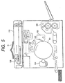
- an original copy G is placed on an original copy holder 110 with the face to be copied being directed downward.
- Copying operation is started by pressing a start button.
- a unit 109 comprising an original-irradiating lamp, a short focus lens array, and a CCD sensor which are combined together, scans the original copy with the irradiation light beam.
- the projected scanning light is formed into an image by the short focus lens array, and is introduced to the CCD sensor.
- the CCD sensor is constituted of a light-receiving portion, a transmission portion, and an output portion. In the CCD light-receiving portion, the optical signals are converted to electric signals. The converted signals are synchronized with a clock pulse and are transmitted successively to the output portion.
- the charge signals are converted to voltage signals, amplified, reduced in impedance, and output.
- the obtained analog signals are converted to digital signals, and are further treated for image formation to optimize the resolution and gradation for the desired image characteristics.
- the treated digital signals are transmitted to a printer portion.
- a latent image is formed in accordance with the image signals as follows.
- the photosensitive drum 101 rotates around a center supporting axis at a prescribed peripheral speed. In the process of rotation, the drum is positively or negatively charged uniformly at a prescribed voltage by a charging device 103.
- the uniformly charged surface is scanned with a light beam of a solid laser element turned on and off in corresponding with the image signal by means of a polygon mirror rotating at a high speed to form a latent image successively on the face of the photosensitive drum 101 corresponding to the original copy.
- the apparatus is provided with a pre-exposure means 102, a charging means 103, a development means 104, a cleaning means 105, and a fixing means 106.
- Fig. 6 illustrates a color copying machine of the present invention.
- an image scanner potion 201 reads the original copy and converts the information into digital signals.
- a printer portion 200 outputs the image having been read by an image scanner 201 in full color onto a paper sheet.
- an original copy-pressing plate 202 serves to fix an original copy 204 on an original copy holding glass plate 203 (hereinafter referred to as a platen).
- the original copy 204 is irradiated with light from an halogen lamp 205.
- the light reflected by the original copy 204 is introduced to mirrors 206, 207, and forms an image through a lens 208 on a three-line sensor 210 constituted of three CCD line sensors (hereinafter referred to as a CCD).
- the CCD 210 separates the full-color optical information from the original copy into color components of red (R), green (G), and blue (B), and transmits the color components to a signal treating portion 209.
- auxiliary scanning direction perpendicular to the electrical scanning direction
- a standard white board 211 is employed at shading correction to produce data for correcting the read-out data of the line sensors 210-2, 210-3, and 210-4 corresponding respectively to the components of R, G, and B.
- This standard white board has uniform spectral reflection characteristics to visible light.
- the output data of the R, G, and B visible sensors 210-2, 210-3, and 210-4 are corrected by use of the standard white board.
- the signal treating portion 209 treats electrically the signal to separate the signals into components of magenta (M), cyan (C), yellow (Y), and black (Bk), and transmits them to a printer portion 200. For one scanning of the original copy in the image scanning portion, respective color components of M, C, Y, and Bk are transmitted successively to the printer 200 for one color-picture image formation by four separate color scanning steps.
- M magenta
- C cyan
- Y yellow
- Bk black
- the image signals of M, C, Y, and Bk from the image scanning portion 201 are transmitted to a laser driver 212.
- the laser driver 212 modulates and drives a semiconductor laser 213 in accordance with the image signal.
- the laser light is allowed to scan a photosensitive drum 217 through a polygon mirror 214, an f- ⁇ lens 215, and a mirror 216.
- Development devices 219-222 are constituted of a magenta development device 219, a cyan development device 220, a yellow development device 221, and a black development device 222.
- the four development devices are successively brought into contact with the photosensitive drum to develop the latent images of M, C, Y and Bk formed on the photosensitive drum 217 with the corresponding toner.
- a transfer drum 223 Onto a transfer drum 223, a paper sheet is delivered from a paper sheet cassette 224, or 225.
- the toner image developed on the photosensitive drum 217 is transferred onto the paper sheet.
- the paper sheet is passed through a fixation unit 226 to have the image fixed, and is driven out of the apparatus.
- the fluorine-modified organic silicone resins were synthesized as shown below. In Examples and Comparative Examples, the unit “part(s)" is based on weight unless otherwise specified.
- a mixture of 24 g of water and 90 g of toluene was placed in a flask.
- a liquid mixture of 23 g of heptadecafluorodecyltrichlorosilane represented by the formula C 8 F 17 C 2 H 4 SiCl 3 , 101 g of diphenyldichlorosilane, and 120 g of toluene was added dropwise with stirring.
- a mixture of 24 g of water and 70 g of toluene was placed in a flask.
- a liquid mixture of 23 g of heptadecafluorodecyltrichlorosilane represented by the formula C 8 F 17 C 2 H 4 SiCl 3 , 71 g of diphenyldichlorosilane, 25 g of phenyltrichlorosilane, and 120 g of toluene was added dropwise with stirring.
- a mixture of 10 g of water, 3 g of isopropanol, and 20 g of toluene was placed in a flask.
- a liquid mixture of 11.4 g of C 4 F 9 C 2 H 4 SiCl 3 , 2.6 g of (CH 3 ) 2 SiCl 2 , 27.5 g of phenyltrichlorosilane, and 30 g of toluene was added dropwise with stirring.
- a fluorine-modified organic silicone resin represented by the formula: ⁇ F(CF 2 ) 4 C 2 H 4 SiO) 3/2 ⁇ x ⁇ (CH 3 ) 2 SiO 2/2 ⁇ y1 ⁇ (C 6 H 5) SiO 3/2 ⁇ y2 where x is 1 on average, y1 is 1 on average, and y2 is 6 on average.
- This resin was a white solid having a softening point of 50-60°C, and a weight-average molecular weight of 4.9 ⁇ 10 4 .
- a mixture of 20 g of water, and 90 g of toluene was placed in a flask.
- a liquid mixture of 4.7 g of (CF 3 )C 2 H 4 SiCl 3 , 11.6 g of C 8 F 17 C 2 H 4 SiCl 3 , 5.6 g of (CH 3 ) 3 SiCl, 75.9 g of diphenyldichlorosilane, and 120 g of toluene was added dropwise with stirring.
- a fluorine-modified organic silicone resin represented by the formula: ⁇ (CF 3 )C 2 H 4 SiO 3/2 ⁇ x1 ⁇ F(CF 2 ) 8 C 2 H 4 SiO 3/2 ⁇ x2 - ⁇ (CH 3 ) 3 SiO 1/2 ⁇ y1 ⁇ (C 6 H 5 ) 2 SiO 2/2 ⁇ y2 where x1 is 1 on average, x2 is 1 on average, y1 is 3 on average, and y2 is 13 on average.
- This resin was a white solid having a softening point of 60-70°C, and a weight-average molecular weight of 8.4 ⁇ 10 3 .
- a mixture of 24 g of aqueous 36% (weight) hydrochloric acid, and 100 g of toluene was placed in a flask.
- a liquid mixture of 11.5 g of C 8 F 17 C 2 H 4 SiCl 3 , 11.0 g of (CH 3 ) 3 SiCl, 25.1 g of diphenyldichlorosilane, 20.4 g of Si(OC 2 H 5 ) 4 , and 100 g of toluene was added dropwise with stirring.
- a fluorine-modified organic silicone resin represented by the formula: ⁇ F(CF 2 ) 8 C 2 H 4 SiO 3/2 ⁇ x ⁇ (CH 3 ) 3 SiO 1/2 ⁇ y1 - ⁇ (C 6 H 5 ) 2 SiO 2/2 ⁇ y2 ⁇ SiO 4/2 ⁇ y3 where x is 1 on average, y1 is 5 on average, y2 is 5 on average, and y3 is 6 on average.
- This resin was a white solid having a softening point of not lower than 200°C, and a weight-average molecular weight of 4.5 ⁇ 10 3 .
- the resin prepared in Synthesis Example 1, 4-[2-(triethoxysilyl)ethyl]triphenylamine, and a polycarbonate resin (trade name: Z-200, Mitsubishi Gas Chemical Co., Inc.) were dissolved in THF in a solid content of 20%, 40%, and 40% by weight.
- the solution was applied onto a glass plate by a bar coater, and was dried at 120°C for one hour, obtaining a uniform transparent film of 10 ⁇ m thick.
- the uniformity of the film was confirmed by microscopic examination.
- This sample was transparent, and showed an absorbance of 0.001 per ⁇ m thickness at 600 nm by spectrophotometry.
- the contact angle with water was 105°, showing a lower surface energy of the sample.
- the resin prepared in Synthesis Example 2 4-[2-(triethoxysilyl)ethyl]triphenylamine, and a polycarbonate resin (trade name: Z-200, Mitsubishi Gas Chemical Co., Inc.) were dissolved in THF in a solid content of 20%, 40%, and 40% by weight.
- the solution was applied onto a glass plate by a bar coater, and was dried at 120°C for one hour, obtaining a uniform transparent film of 10 ⁇ m thick.
- the uniformity of the film was confirmed by microscopic examination.
- This sample was transparent, and showed an absorbance of 0.001 per ⁇ m thickness at 600 nm by spectrophotometry.
- the contact angle with water was 107°, showing a lower surface energy of the sample.
- a mirror-polished aluminum cylinder of 60 mm in outside diameter was coated with alumite by anodic oxidation. This cylinder was used as the electroconductive support.
- a coating liquid for a charge-generating layer was prepared by dispersing 5 parts of the bisazo pigment shown by the formula below in a solution of 2 parts of polyvinylbenzal (benzal-modified degree of 75% of higher) in 95 parts of cyclohexanone by a sand mill for 20 hours. On the subbing layer (or alumite) formed above, the charge-generating layer was formed by applying this liquid dispersion by immersion coating in a dry thickness of 0.2 ⁇ m.
- a coating liquid for a charge-transporting layer was prepared by dissolving 5 parts of the triarylamine represented by the structural formula below, 2.5 parts of the resin prepared in Synthesis Example 1, and 5 parts of a polycarbonate resin (trade name; Z-400, Mitsubishi Gas Chemical Co., Inc.) in 70 parts of tetrahydrofuran. This solution was applied on the charge-generating layer in a dry thickness of 12 ⁇ m by immersion coating to form the charge-transporting layer.
- the obtained photosensitive member was tested for the electrophotographic characteristics at a wavelength of 680 nm by charging at -700 V.
- E 1/2 light exposure to decrease the charged voltage to -350 V
- the residual potential was 48 V, thus the results were good.
- This electrophotographic photosensitive member was set on a digital copying machine GP55 (roller charging system, manufactured by Canon K.K.) which had been modified to give the aforementioned irradiation spot diameter.
- the copied image was evaluated at the initial charging -400 V.
- the image output was sufficiently uniform from the initial stage through 5000-sheet copying in the duration test; the gradation reproducibility was excellent to give 256 gradations at 400 dpi; and the abrasion of the photosensitive member was as small as 0.4 ⁇ m per 1000-sheet duration test.
- the contact angle with water on the surface of the photosensitive member was found to be 104° at the initial stage, and 98° at the time of 5000-sheet copying.
- a mirror-polished aluminum cylinder of 80 mm in outside diameter coated with alumite by anodic oxidation was used, on which a charge-generating layer and a charge-transporting layer were formed in the same manner as in Example 3 to prepare an electrophotographic photosensitive member.
- This electrophotographic photosensitive member was set on a digital copying machine CLC500 (corona charging system, manufactured by Canon K.K.) which had been modified to give the aforementioned irradiation spot diameter.
- CLC500 corona charging system, manufactured by Canon K.K.
- the copied image was evaluated at the initial charging -400 V.
- the image output was sufficiently uniform from the initial stage through the 5000-sheet copying duration test; the gradation reproducibility was excellent to give 256 gradations at 400 dpi; and the abrasion of the photosensitive member was as small as 0.2 ⁇ m per 1000-sheet duration test.
- the contact angle with water on the surface of the photosensitive member was found to be 104° at the initial stage, and 94° at the time of 5000-sheet copying.
- a liquid dispersion for an electroconductive layer was prepared by dispersing 200 parts of ultrafine particulate electroconductive barium sulfate (primary particle diameter: 50 nm) and 3 parts of particulate silicone resin (average particle diameter: 2 ⁇ m) in a solution of 167 parts of a phenol resin (trade name: Priophen, Dainippon Ink and Chemicals, Inc.) in 100 parts of methylcellosolve.
- This dispersion was applied on a drawn aluminum cylinder of 30 mm in outside diameter by immersion coating to form an electroconductive layer in a dry thickness of 15 ⁇ m.
- alcohol-soluble copolymer nylon trade name: Amylan CM-8000, Toray Industries, Inc.
- a dispersion for a charge-generating layer was prepared by dispersing 5 parts of I-type oxytitanium phthalocyanine pigment in a solution of 2 parts of polyvinylbenzal (benzal-modified degree: 75% or higher) in 95 part of cyclohexanone by a sand mill for 2 hours. This dispersion was applied onto the above subbing layer by immersion coating to form a charge-generating layer in a dry thickness of 0.2 ⁇ m.
- a solution for a charge-transporting layer was prepared by dissolving 27.5 parts of the fluorine-modified organic silicone resin prepared in Synthesis Example 2, 55 parts of the triarylamine used in Example 3, and 55 parts of a polycarbonate resin (trade name: Z-400, Mitsubishi Gas Chemical Co., Inc.) in 70 parts of tetrahydrofuran. This solution was applied on the above charge-generating layer by immersion coating to form a charge-transporting layer in a dry thickness of 10 ⁇ m.
- the contact angle with water was 105°.
- the obtained photosensitive member was tested for the electrophotographic characteristics at a wavelength of 680 nm by charging at -700 V.
- E 1/2 light exposure to decrease the charged voltage to -350 V
- the residual potential was 45 V, thus the results were good.
- This electrophotographic photosensitive member was set on a laser beam printer P270 having an AC roller charger (manufactured by Canon K.K.) which had been modified to give the aforementioned irradiation spot diameter.
- an image was formed and the copied image was evaluated at the initial charging -500 V.
- the abrasion of the photosensitive member was as small as 2 ⁇ m or less; the contact angle with water was 100° desirably; no image deterioration was observed; and one pixel reproducibility at a highlight portion was sufficient in input signals corresponding to 600 dpi.
- a liquid dispersion for an electroconductive layer was prepared by dispersing 200 parts of ultrafine particulate electroconductive barium sulfate (primary particle diameter: 50 nm) in a solution of 167 parts of a phenol resin (trade name: Priophen, Dainippon Ink and Chemicals, Inc.) in 100 parts of methylcellosolve. This dispersion was applied on a drawn aluminum cylinder of 30 mm in outside diameter by immersion coating in the same manner as in Example 7 to form an electroconductive layer in a dry thickness of 10 ⁇ m.
- a solution for a charge-transporting layer was prepared by dissolving 5 parts of the triarylamine employed in example 3 and 5 parts of a polycarbonate resin (trade name: Z-400, Mitsubishi Gas Chemical Co., Inc.) in 70 parts of chlorobenzene. This solution was applied on the above charge-generating layer by immersion coating to form a charge-transporting layer in a dry thickness of 8 ⁇ m.
- Example 2 Onto the above charge-transporting layer, a resin solution prepared in Example 2 was applied by spray coating to form a film having a dry thickness of 4 ⁇ m. The formed film was dried and thermally cured at 110°C for 2 hours to complete the photosensitive member of the present invention.
- the contact angle with water was 109°.
- the obtained photosensitive member was tested for the electrophotographic characteristics at a wavelength of 680 nm by charging at -700 V.
- E 1/2 light exposure to decrease the charged voltage to -350 V
- the residual potential was 39 V, thus the results were good.
- This electrophotographic photosensitive member was set on a laser beam printer P270 (manufactured by Canon K.K.) which had been modified in the optical system such that a semiconductor laser of 780 nm and 100 mW was employed to give the laser spot diameter of 60x20 ⁇ m 2 .
- a laser beam printer With this laser beam printer, an image was formed and the copied image was evaluated at the initial charging -500 V.
- the abrasion of the photosensitive member was as small as 2.5 ⁇ m or less; the contact angle with water was 98° desirably; no image deterioration such as black dots caused by charge injection or interference fringes was observed; and one pixel reproducibility at a highlight portion was sufficient in input signals corresponding to 600 dpi.
- a liquid dispersion for an electroconductive layer was prepared by dispersing 200 parts of ultrafine particulate electroconductive barium sulfate (primary particle diameter: 50 nm) and 3 parts of particulate silicone resin (average particle diameter: 2 ⁇ m) in a solution of 167 parts of a phenol resin (trade name: Priophen, Dainippon Ink and Chemicals, Inc.) in 100 parts of methylcellosolve.
- This dispersion was applied on a drawn aluminum cylinder of 30 mm in outside diameter by immersion coating to form an electroconductive layer in a dry thickness of 15 ⁇ m.
- an alcohol-soluble copolymer nylon trade name: Amylan CM-8000, Toray Industries, Inc.
- a dispersion for a charge-generating layer was prepared by dispersing 5 parts of I-type oxytitanium phthalocyanine pigment in a solution of 2 parts of polyvinylbenzal (benzal-modified degree: 75% or higher) in 95 part of cyclohexanone by a sand mill for 2 hours. This dispersion was applied onto the above subbing layer by immersion coating to form a charge-generating layer in a dry thickness of 0.2 ⁇ m.
- a solution for a charge-transporting layer was prepared by dissolving 27.5 parts of the fluorine-modified organic silicone resin prepared in Synthesis Example 2, 55 parts of the triarylamine used in Example 4, and 55 parts of a polycarbonate resin (trade name: Z-400, Mitsubishi Gas Chemical Co., Inc.) in 70 parts of tetrahydrofuran. This solution was applied on the above charge-generating layer by immersion coating to form a charge-transporting layer in a dry thickness of 20 ⁇ m.
- the contact angle with water was 105°.
- the obtained photosensitive member was tested for the electrophotographic characteristics at a wavelength of 680 nm by charging at -700 V.
- E 1/2 light exposure to decrease the charged voltage to -350 V
- the residual potential was 51 V, thus the results were good.
- This electrophotographic photosensitive member was set on a laser beam printer P270 having an AC roller (manufactured by Canon K.K.) which had been modified in the irradiation spot conditions as above. With this apparatus, an image was formed and the copied image was evaluated at the initial charging -500 V. After the 4000-sheet duration test, the abrasion of the photosensitive member was as small as 2 ⁇ m or less; the contact angle with water was 100° desirably; and no image deterioration was observed. However, one pixel reproducibility at a highlight portion was a little in sufficient in input signal corresponding to 600 dpi.
- a liquid dispersion for an electroconductive layer was prepared by dispersing 200 parts of ultrafine particulate electroconductive barium sulfate (primary particle diameter: 50 nm) and 3 parts of particulate silicone resin (average particle diameter: 2 ⁇ m) in a solution of 167 parts of a phenol resin (trade name: Priophen, Dainippon Ink and Chemicals, Inc.) in 100 parts of methylcellosolve.
- This dispersion was applied on a drawn aluminum cylinder of 30 mm in outside diameter by immersion coating to form an electroconductive layer in a dry thickness of 15 ⁇ m.
- an alcohol-soluble copolymer nylon trade name: Amylan CM-8000, Toray Industries, Inc.
- a dispersion for a charge-generating layer was prepared by dispersing 5 parts of I-type oxytitanium phthalocyanine pigment in a solution of 2 parts of polyvinylbenzal (benzal-modified degree: 75% or higher) in 95 parts of cyclohexanone by a sand mill for 2 hours. This dispersion was applied onto the above subbing layer by immersion coating to form a charge-generating layer in a dry thickness of 0.2 ⁇ m.
- a solution for a charge-transporting layer was prepared by dissolving 47.0 parts of the fluorine-modified organic silicone resin prepared in Synthesis Example 3, 55 parts of the triarylamine used in Example 4, and 55 parts of a polycarbonate resin (trade name: Z-400, Mitsubishi Gas Chemical Co., Inc.) in 150 parts of tetrahydrofuran. This solution was applied on the above charge-generating layer by immersion coating to form a charge-transporting layer in a dry thickness of 12 ⁇ m.
- the contact angle with water was 102°.
- the obtained photosensitive member was tested for the electrophotographic characteristics at a wavelength of 680 nm by charging at -550 V.
- E 1/2 light exposure to decrease the charged voltage to -275 V
- the residual potential was 30 V, thus the results were good.
- This electrophotographic photosensitive member was set on a laser beam printer P270 having an AC roller (manufactured by Canon K.K.) which had been modified in the irradiation spot conditions as above. With this apparatus, an image was formed and the copied image was evaluated at the initial charging -500 V. After the 4000-sheet duration test, the abrasion of the photosensitive member was as small as 2 ⁇ m or less; the contact angle with water was 90° desirably; and no image deterioration was observed.
- a liquid dispersion for an electroconductive layer was prepared by dispersing 200 parts of ultrafine particulate electroconductive barium sulfate (primary particle diameter: 50 nm) and 3 parts of particulate silicone resin (average particle diameter: 2 ⁇ m) in a solution of 167 parts of a phenol resin (trade name: Priophen, Dainippon Ink and Chemicals, Inc.) in 100 parts of methylcellosolve.
- This dispersion was applied on a drawn aluminum cylinder of 30 mm in outside diameter by immersion coating to form an electroconductive layer in a dry thickness of 15 ⁇ m.
- an alcohol-soluble copolymer nylon trade name: Amylan CM-8000, Toray Industries, Inc.
- a dispersion for a charge-generating layer was prepared by dispersing 5 parts of I-type oxytitanium phthalocyanine pigment in a solution of 2 parts of polyvinylbenzal (benzal-modified degree: 75% or higher) in 95 parts of cyclohexanone by a sand mill for 2 hours. This dispersion was applied onto the above subbing layer by immersion coating to form a charge-generating layer in a dry thickness of 0.2 ⁇ m.
- a solution for a charge-transporting layer was prepared by dissolving 70 parts of the fluorine-modified organic silicone resin prepared in Synthesis Example 4, 55 parts of the triarylamine used in Example 4, and 55 parts of a polycarbonate resin (trade name: Z-400, Mitsubishi Gas Chemical Co., Inc.) in 150 parts of tetrahydrofuran. This solution was applied on the above charge-generating layer by immersion coating to form a charge-transporting layer in a dry thickness of 15 ⁇ m.
- the contact angle with water was 112°.
- the obtained photosensitive member was tested for the electrophotographic characteristics at a wavelength of 680 nm by charging at -700 V.
- E 1/2 light exposure to decrease the charged voltage to -350 V
- the residual potential was 40 V, thus the results were good.
- This electrophotographic photosensitive member was set on a laser beam printer P270 having an AC roller (manufactured by Canon K.K.) which had been modified in the irradiation spot conditions as above. With this apparatus, an image was formed at the initial charging of -500 V and the copied image was evaluated. After the 4000-sheet duration test, the abrasion of the photosensitive member was as small as 3 ⁇ m or less; the contact angle of water was 100° desirably; and no image deterioration was observed.
- a liquid dispersion for an electroconductive layer was prepared by dispersing 200 parts of ultrafine particulate electroconductive barium sulfate (primary particle diameter: 50 nm) and 3 parts of particulate silicone resin (average particle diameter: 2 ⁇ m) in a solution of 167 parts of a phenol resin (trade name: Priophen, Dainippon Ink and Chemicals, Inc.) in 100 parts of methylcellosolve.
- This dispersion was applied on a drawn aluminum cylinder of 30 mm in outside diameter by immersion coating to form an electroconductive layer in a dry thickness of 15 ⁇ m.
- an alcohol-soluble copolymer nylon trade name: Amylan CM-8000, Toray Industries, Inc.
- a dispersion for a charge-generating layer was prepared by dispersing 5 parts of I-type oxytitanium phthalocyanine pigment in a solution of 2 parts of polyvinylbenzal (benzal-modified degree: 75% or higher) in 95 parts of cyclohexanone by a sand mill for 2 hours. This dispersion was applied onto the above subbing layer by immersion coating to form a charge-generating layer in a dry thickness of 0.2 ⁇ m.
- a solution for a charge-transporting layer was prepared by dissolving 20 parts of the fluorine-modified organic silicone resin prepared in Synthesis Example 5, 55 parts of the triarylamine used in Example 4, and 55 parts of a polycarbonate resin (trade name: Z-400, Mitsubishi Gas Chemical Co., Inc.) in 150 parts of tetrahydrofuran. This solution was applied on the above charge-generating layer by immersion coating to form a charge-transporting layer in a dry thickness of 12 ⁇ m.
- the contact angle with water was 108°.
- the obtained photosensitive member was tested for the electrophotographic characteristics at a wavelength of 680 nm by charging at -550 V.
- E 1/2 light exposure to decrease the charged voltage to -275 V
- the residual potential was 28 V, thus the results were good.
- This electrophotographic photosensitive member was set on a laser beam printer P270 having an AC roller (manufactured by Canon K.K.) which had been modified in the irradiation spot conditions as above. With this apparatus, an image was formed at the initial charge -500 V and the copied image was evaluated. After the 4000-sheet duration test, the abrasion of the photosensitive member was as small as 3 ⁇ m or less; the contact angle of water was 93° desirably; and no image deterioration was observed.
- Fine particulate teflon (trade name: Lubron LD-1, Daikin Industries, Ltd., particle diameter: about 0.2 ⁇ m), 4-[2-(triethoxysilyl)ethyl]triphenylamine, and a polycarbonate resin (trade name: Z-200, Mitsubishi Gas Chemical Co., Inc.) were dissolved in THF in a solid content of 5%, 47.5%, and 47.5% by weight.
- the solution was applied onto a glass plate by a bar coater, and dried at 120°C for one hour, to obtaining a white-turbid film of 10 ⁇ m thick.
- the aggregate of the teflon particles was observed by microscopic examination.
- This sample showed a light absorbance of 0.022 per ⁇ m thickness at 600 nm by spectrophotometry, and considerable light scattering was observed.
- the contact angle with water was 86°, showing an insufficient lowering of the surface energy of the sample.
- the solution was applied onto a glass plate by a bar coater, and dried at 120°C for one hour, obtaining a white-turbid film of 10 ⁇ m thick which was uneven (or concave and convex) in its surface.
- the aggregate of the teflon particles was observed by microscopic examination.
- This sample showed a light absorbance of 0.05 per m thickness at 600 nm by spectrophotometry, and considerable light scattering was observed.
- the contact angle with water was 103°, showing that the surface energy of the sample was reduced.
- the solution was applied onto a glass plate by a bar coater, and was dried at 120°C for one hour, to obtaining a white-turbid film of 10 ⁇ m thick.
- This sample showed a light absorbance of 0.012 per ⁇ m thickness at 600 nm by spectrophotometry, and considerable light scattering was observed.
- the contact angle with water was 88°, showing insufficient lowering of the surface energy of the sample.
- the solution was applied onto an aluminum plate of 50 ⁇ m thick by a bar coater, and dried at 120°C for one hour, obtaining a uniform transparent film of 20 ⁇ m thick.
- the uniformity of the film was confirmed by microscopic examination.
- An electroconductive rubber roller was brought into contact with the resin film of this sample, and using the aluminum plate as an earth, an AC voltage of 1500 Hz having a peak-to-peak voltage of 1500 V superposed on a DC voltage of -600 V was applied to the electroconductive roller for one hour to test the deterioration caused by the electric charging.
- the resistance to discharge was evaluated by the depth of a hollow formed by electric discharge in the vicinity of the portion at which the roller was brought into contact with the resin film.
- the depth of the concave formed on the film was as large as 1 ⁇ m.
- a solution for a charge-transporting layer was prepared by dissolving 5 parts of the triarylamine employed in Example 4 and 5 parts of a polycarbonate resin (trade name: Z-400, Mitsubishi Gas Chemical Co., Inc.) in 70 parts of chlorobenzene. This solution was applied on the above charge-generating layer by immersion coating to form a charge-transporting layer in a dry thickness of 12 ⁇ m.
- the photosensitive member was evaluated for image formation by means of the same laser beam printer (manufactured by Canon K.K.) as the one employed in Example 4.
- a liquid dispersion for an electroconductive layer was prepared by dispersing 200 parts of ultrafine particulate electroconductive barium sulfate (primary particle diameter: 50 nm) and 3 parts of particulate silicone resin (average particle diameter: 2 ⁇ m) in a solution of 167 parts of a phenol resin (trade name: Priophen, Dainippon Ink and Chemicals, Inc.) in 100 parts of methylcellosolve.
- This dispersion was applied on a drawn aluminum cylinder of 30 mm in outside diameter by immersion coating to form an electroconductive layer of a dry thickness of 15 ⁇ m.
- alcohol-soluble copolymer nylon trade name: Amylan CM-8000, Toray Industries, Inc.
- a dispersion for a charge-generating layer was prepared by dispersing 5 parts of I-type oxytitanium phthalocyanine pigment in a solution of 2 parts of polyvinylbenzal (benzalation degree: 75% or higher) in 95 parts of cyclohexanone by a sand mill for 2 hours. This dispersion was applied onto the above subbing layer by immersion coating to form a charge-generating layer in a dry thickness of 0.2 ⁇ m.
- a solution for a charge-transporting layer was prepared by dispersing and dissolving 5 parts of the triarylamine employed in Example 4, 5 parts of a polycarbonate resin (trade name: Z-400, Mitsubishi Gas Chemical Co., Inc.), and 0.5 part of fine particulate teflon in 70 parts of chlorobenzene. This solution was applied on the above charge-generating layer by immersion coating to form a charge-transporting layer in a dry thickness of 12 ⁇ m.
- the photosensitive member was evaluated for image formation by means of the same laser beam printer (manufactured by Canon K.K.) as the one employed in Example 4.
- the abrasion was about 4 ⁇ m; the contact angle was 89°, showing that the surface energy was slightly reduced; and one pixel reproducibility was insufficient and non-uniform in the highlight portion at 600 dpi from the initial stage of the duration test.
Landscapes
- Physics & Mathematics (AREA)
- Chemical & Material Sciences (AREA)
- General Physics & Mathematics (AREA)
- Chemical Kinetics & Catalysis (AREA)
- Spectroscopy & Molecular Physics (AREA)
- Inorganic Chemistry (AREA)
- Photoreceptors In Electrophotography (AREA)
Claims (6)
- Ein elektrofotographisches lichtempfindliches Element mit einer lichtempfindlichen Schicht, die eine Ladungserzeugungsschicht und eine Ladungstransportschicht in dieser Reihenfolge auf einem Träger umfasst, wobei eine Oberflächenschicht des lichtempfindlichen Elements ein fluoriertes Polysiloxan enthält,
die Oberflächenschicht ferner ein Bindemittelharz enthält;
das fluorierte Polysiloxan ein fluormodifiziertes organisches Silikonharz ist, das durch die folgende Formel (I) der durchschnittlichen Einheiten dargestellt ist, wobei der Erweichungspunkt des fluormodifizierten organischen Silikonharzes nicht geringer als 30°C ist:
{[F(CF2)a1-Q1][R1]m1SiO(3-m1)/2}x1{[F(CF2)a2-Q2][R2]m2 SiO(3-m2)/2}x2•••{[F(CF2)ap-Qp][Rp]mpSiO(3-mp)/2}xp{R1'n1 SiO(4-n1)/2}y1{R2'n2SiO(4-n2)/2}y2•••{Rq'nqSiO(4-nq)/2]yq
wobei R1, ••• und Rp, R1' , ••• und Rq' jeweils eine Alkyl- oder Arylgruppe sind; Q1, ••• und Qp jeweils eine Alkylengruppe sind; m1, ••• und mp jeweils eine ganze Zahl von 0 bis 2 sind; n1, ••• und nq jeweils eine ganze Zahl von 0 bis 3 sind; a1, ••• und ap jeweils eine ganze Zahl sind; x1 und y1 jeweils eine Zahl größer als 0 sind; und x2, ••• und xp, und y2, ••• und yq jeweils eine Zahl von 0 oder mehr sind;
wobei das fluorinierte Polysiloxan eine vernetzte Struktur aufweist und ein gewichtsgemittetes Molekulargewicht von 1.000 bis 100.000 besitzt. - Das elektrofotographische lichtempfindliche Element gemäß Anspruch 1, wobei die Oberflächenschicht eine Ladungstransportschicht ist.
- Das elektrofotographische lichtempfindliche Element gemäß Anspruch 1, wobei die Oberflächenschicht eine Schutzschicht ist.
- Das elektrofotographische lichtempfindliche Element gemäß Anspruch 1, wobei R1, ••• und Rp, R1' , ••• und Rq' jeweils eine Gruppe von 1-12 Kohlenstoffen sind; Q1, ••• und Qp jeweils eine Gruppe von 2-6 Kohlenstoffen sind; und das Verhältnis von (x1 + x2 + ••• + xp): (y1 + y2 + ••• + yq) im Bereich von 1:20 bis 1:5 liegt.
- Ein elektrofotographisches Gerät, welches das elektrofotographische lichtempfindliche Element wie es in irgendeinem der Ansprüche 1 bis 4 angeführt ist, eine Ladungseinrichtung zur Ladung des elektrofotographischen lichtempfindlichen Elements und eine Bildbelichtungseinrichtung zur Belichtung des geladenen elektrofotographischen lichtempfindlichen Elements mit Bildlicht zur Erzeugung eines elektrostatischen latenten Bildes, und eine Entwicklungseinrichtung zur Entwicklung des erzeugten elektrostatischen latenten Bildes mit einem Toner umfasst.
- Eine Verfahrenskartusche, in welcher das elektrofotographische lichtempfindliche Element wie es in irgendeinem der Ansprüche 1 bis 4 angeführt ist und wenigstens eine Einrichtung, ausgewählt aus einer Ladungseinrichtung, einer Entwicklungseinrichtung und einer Reinigungseinrichtung, miteinander kombiniert in einer Einheit vorliegen.
Applications Claiming Priority (2)
| Application Number | Priority Date | Filing Date | Title |
|---|---|---|---|
| JP142835/96 | 1996-06-05 | ||
| JP14283596 | 1996-06-05 |
Publications (4)
| Publication Number | Publication Date |
|---|---|
| EP0811885A2 EP0811885A2 (de) | 1997-12-10 |
| EP0811885A3 EP0811885A3 (de) | 1998-02-11 |
| EP0811885B1 true EP0811885B1 (de) | 2006-01-04 |
| EP0811885B8 EP0811885B8 (de) | 2006-04-26 |
Family
ID=15324728
Family Applications (1)
| Application Number | Title | Priority Date | Filing Date |
|---|---|---|---|
| EP97109011A Expired - Lifetime EP0811885B8 (de) | 1996-06-05 | 1997-06-04 | Elektrophotographisches, lichtempfindliches Element, sowie ein elektrophotographisches Gerät und eine Prozesskassette die es umfassen |
Country Status (3)
| Country | Link |
|---|---|
| US (1) | US5905008A (de) |
| EP (1) | EP0811885B8 (de) |
| DE (1) | DE69735036T2 (de) |
Families Citing this family (20)
| Publication number | Priority date | Publication date | Assignee | Title |
|---|---|---|---|---|
| US6203954B1 (en) * | 1998-06-30 | 2001-03-20 | Canon Kabushiki Kaisha | Electrophotographic photosensitive member process cartridge and electrophotographic apparatus |
| JP2001034003A (ja) * | 1999-07-19 | 2001-02-09 | Minolta Co Ltd | 電子写真感光体 |
| US6395441B1 (en) * | 1999-12-28 | 2002-05-28 | Canon Kabushiki Kaisha | Electrophotographic photosensitive member, process cartridge and electrophotographic apparatus |
| JP2001337467A (ja) * | 2000-05-25 | 2001-12-07 | Fuji Denki Gazo Device Kk | 電子写真感光体 |
| US6517984B1 (en) | 2001-03-27 | 2003-02-11 | Heidelberger Druckmaschinen Ag | Silsesquioxane compositions containing tertiary arylamines for hole transport |
| US7139492B2 (en) * | 2001-12-11 | 2006-11-21 | Toshiba Tec Kabushiki Kaisha | Imaging forming apparatus having a plurality of dismountable units necessary for image forming |
| JP2004021188A (ja) * | 2002-06-20 | 2004-01-22 | Konica Minolta Holdings Inc | 画像形成装置 |
| JP4134753B2 (ja) * | 2002-06-26 | 2008-08-20 | 富士ゼロックス株式会社 | 電子写真用感光体、電子写真用部材、プロセスカートリッジ、及び画像形成装置 |
| EP1533658B1 (de) * | 2002-06-28 | 2013-09-04 | Canon Kabushiki Kaisha | Lichtempfindlicher körper für die elektrofotografie, entwicklungskassette und elektrofotografische vorrichtung |
| US7700248B2 (en) * | 2002-07-08 | 2010-04-20 | Eastman Kodak Company | Organic charge transporting polymers including charge transport moieties and silane groups, and silsesquioxane compositions prepared therefrom |
| US6991880B2 (en) * | 2002-07-23 | 2006-01-31 | Xerox Corporation | Imaging members |
| JP3814628B2 (ja) * | 2004-05-20 | 2006-08-30 | キヤノン株式会社 | 画像形成装置 |
| TW200625035A (en) * | 2005-01-07 | 2006-07-16 | Sinonar Corp | Electrophotographic photoreceptor |
| US7541122B2 (en) * | 2006-07-12 | 2009-06-02 | Xerox Corporation | Photoconductor having silanol-containing charge transport layer |
| US7560206B2 (en) * | 2006-07-12 | 2009-07-14 | Xerox Corporation | Photoconductors with silanol-containing photogenerating layer |
| US7670734B2 (en) * | 2006-08-30 | 2010-03-02 | Xerox Corporation | Titanyl phthalocyanine silanol terphenyl photoconductors |
| US7718332B2 (en) * | 2006-08-30 | 2010-05-18 | Xerox Corporation | Titanyl phthalocyanine silanol photoconductors |
| US7618758B2 (en) * | 2006-08-30 | 2009-11-17 | Xerox Corporation | Silanol containing perylene photoconductors |
| JP7752992B2 (ja) | 2021-08-06 | 2025-10-14 | キヤノン株式会社 | 電子写真装置 |
| JP7752991B2 (ja) | 2021-08-06 | 2025-10-14 | キヤノン株式会社 | 電子写真装置 |
Family Cites Families (13)
| Publication number | Priority date | Publication date | Assignee | Title |
|---|---|---|---|---|
| US3859090A (en) * | 1973-05-17 | 1975-01-07 | Eastman Kodak Co | Repellent compositions and elements containing the same |
| JPS5730843A (en) * | 1980-07-31 | 1982-02-19 | Fuji Xerox Co Ltd | Electrophotographic receptor |
| JPS61132954A (ja) * | 1984-11-30 | 1986-06-20 | Hitachi Chem Co Ltd | 電子写真感光体 |
| JPH04324454A (ja) * | 1991-04-24 | 1992-11-13 | Canon Inc | 電子写真感光体及びその製造方法 |
| DE69231531T2 (de) * | 1991-07-22 | 2001-03-15 | Matsushita Electric Industrial Co., Ltd. | Elektrophotographisches Gerät |
| JP3010808B2 (ja) * | 1991-07-26 | 2000-02-21 | 三菱化学株式会社 | 電子写真感光体 |
| US5266431A (en) * | 1991-12-31 | 1993-11-30 | Xerox Corporation | Electrographic imaging members |
| US5242774A (en) * | 1992-03-27 | 1993-09-07 | Xerox Corporation | Photoconductive imaging members with fluorinated polycarbonates |
| US5320923A (en) * | 1993-01-28 | 1994-06-14 | Hewlett-Packard Company | Reusable, positive-charging organic photoconductor containing phthalocyanine pigment, hydroxy binder and silicon stabilizer |
| US5436099A (en) * | 1993-12-21 | 1995-07-25 | Xerox Corporation | Photoreceptor with low surface energy overcoat |
| DE69512575T2 (de) * | 1994-07-06 | 2000-05-04 | Canon K.K., Tokio/Tokyo | Elektrografisches Gerät und Bilderzeugungsverfahren |
| JPH11504728A (ja) * | 1995-04-28 | 1999-04-27 | ミネソタ・マイニング・アンド・マニュファクチャリング・カンパニー | 光導電体用剥離層 |
| US5626998A (en) * | 1995-06-07 | 1997-05-06 | Xerox Corporation | Protective overcoating for imaging members |
-
1997
- 1997-06-02 US US08/867,523 patent/US5905008A/en not_active Expired - Lifetime
- 1997-06-04 DE DE69735036T patent/DE69735036T2/de not_active Expired - Lifetime
- 1997-06-04 EP EP97109011A patent/EP0811885B8/de not_active Expired - Lifetime
Also Published As
| Publication number | Publication date |
|---|---|
| DE69735036T2 (de) | 2006-08-17 |
| EP0811885B8 (de) | 2006-04-26 |
| EP0811885A2 (de) | 1997-12-10 |
| EP0811885A3 (de) | 1998-02-11 |
| DE69735036D1 (de) | 2006-03-30 |
| US5905008A (en) | 1999-05-18 |
Similar Documents
| Publication | Publication Date | Title |
|---|---|---|
| EP0811885B1 (de) | Elektrophotographisches, lichtempfindliches Element, sowie ein elektrophotographisches Gerät und eine Prozesskassette die es umfassen | |
| JP3267519B2 (ja) | 電子写真感光体、該電子写真感光体を有するプロセスカートリッジ及び画像形成装置 | |
| EP0818714B1 (de) | Elektrophotographisches, lichtempfindliches Element, sowie ein elektrophotographischer Apparat und Prozesskassette unter Verwendung desselben | |
| JP2000171990A (ja) | 電子写真感光体とその製造方法及び前記感光体を用いたプロセスカ―トリッジと画像形成装置 | |
| JP2000275886A (ja) | 電子写真感光体、それを用いたプロセスカートリッジ及び画像形成装置 | |
| EP1030223B1 (de) | Elektrophotographischer Photorezeptor, Bildaufzeichnungsgerät, Bildaufzeichnungsverfahren und Prozesskartusche | |
| JP3618962B2 (ja) | 電子写真感光体、この電子写真感光体を用いた電子写真装置及びプロセスカートリッジ | |
| JP2001034001A (ja) | 電子写真感光体、画像形成方法、画像形成装置及びプロセスカートリッジ | |
| JPH11202531A (ja) | 電子写真感光体及び電子写真画像形成装置 | |
| JP3681088B2 (ja) | 電子写真感光体、電子写真装置及びプロセスカートリッジ | |
| JP2000206723A (ja) | 電子写真感光体、プロセスカ―トリッジ及び電子写真装置 | |
| JP4040165B2 (ja) | 電子写真感光体、該電子写真感光体を有するプロセスカートリッジ及び画像形成装置 | |
| HK1005953B (en) | Electrophotographic photosensitive member, and electrophotographic apparatus and process cartridge employing the same | |
| JP4449740B2 (ja) | 有機感光体、プロセスカートリッジ及び画像形成装置 | |
| JP2000242021A (ja) | 電子写真感光体とそれを用いた画像形成装置、画像形成方法及びプロセスカートリッジ | |
| JPH10301318A (ja) | 電子写真感光体、プロセスカートリッジ及び画像形成装置 | |
| JP2006184426A (ja) | 有機感光体、プロセスカートリッジ及び画像形成装置 | |
| JPH11202527A (ja) | 電子写真感光体および電子写真画像形成装置 | |
| JP2004101710A (ja) | 電子写真感光体、該電子写真感光体を有するプロセスカートリッジ及び電子写真装置 | |
| JP2001337477A (ja) | 電子写真感光体、電子写真画像形成方法、電子写真画像形成装置、及びプロセスカートリッジ | |
| JP2000305291A (ja) | 電子写真感光体とそれを用いた画像形成装置、画像形成方法及びプロセスカートリッジ | |
| JPH11202530A (ja) | 電子写真感光体及び電子写真画像形成装置 | |
| JPH11202533A (ja) | 電子写真感光体および電子写真画像形成装置 | |
| JP2001013702A (ja) | 電子写真感光体と、該感光体を用いた電子写真画像形成方法、電子写真画像形成装置、及びプロセスカートリッジ | |
| JP2004045992A (ja) | 電子写真感光体、該電子写真感光体を有するプロセスカートリッジ及び画像形成装置 |
Legal Events
| Date | Code | Title | Description |
|---|---|---|---|
| PUAI | Public reference made under article 153(3) epc to a published international application that has entered the european phase |
Free format text: ORIGINAL CODE: 0009012 |
|
| AK | Designated contracting states |
Kind code of ref document: A2 Designated state(s): DE FR GB IT |
|
| PUAL | Search report despatched |
Free format text: ORIGINAL CODE: 0009013 |
|
| AK | Designated contracting states |
Kind code of ref document: A3 Designated state(s): AT BE CH DE DK ES FI FR GB GR IE IT LI LU MC NL PT SE |
|
| 17P | Request for examination filed |
Effective date: 19980629 |
|
| AKX | Designation fees paid |
Free format text: DE FR GB IT |
|
| RBV | Designated contracting states (corrected) |
Designated state(s): DE FR GB IT |
|
| 17Q | First examination report despatched |
Effective date: 19991108 |
|
| GRAP | Despatch of communication of intention to grant a patent |
Free format text: ORIGINAL CODE: EPIDOSNIGR1 |
|
| RIN1 | Information on inventor provided before grant (corrected) |
Inventor name: MASATOMI, TORU,C/O DOW CORNING TORAY Inventor name: KOBAYASHI, HIDEKI,C/O DOW CORNING TORAY Inventor name: NAGAO, YAYOI C/O Inventor name: HIRAOKA, KEIKO C/O Inventor name: NISHIDA, SHUNICHIRO C/O Inventor name: YOSHINAGA, KAZUO C/O |
|
| GRAS | Grant fee paid |
Free format text: ORIGINAL CODE: EPIDOSNIGR3 |
|
| GRAA | (expected) grant |
Free format text: ORIGINAL CODE: 0009210 |
|
| AK | Designated contracting states |
Kind code of ref document: B1 Designated state(s): DE FR GB IT |
|
| REG | Reference to a national code |
Ref country code: GB Ref legal event code: FG4D |
|
| RIN2 | Information on inventor provided after grant (corrected) |
Inventor name: MASATOMI, TORU,C/O DOW CORNING TORAY Inventor name: KOBAYASHI, HIDEKI,C/O DOW CORNING TORAY Inventor name: NAGAO, YAYOI C/O CANON KABUSHIKI KAISHA Inventor name: HIRAOKA, KEIKO C/O CANON KABUSHIKI KAISHA Inventor name: NISHIDA, SHUNICHIRO C/O CANON KABUSHIKI KAISHA Inventor name: YOSHINAGA, KAZUO C/O CANON KABUSHIKI KAISHA |
|
| REF | Corresponds to: |
Ref document number: 69735036 Country of ref document: DE Date of ref document: 20060330 Kind code of ref document: P |
|
| ET | Fr: translation filed | ||
| PLBE | No opposition filed within time limit |
Free format text: ORIGINAL CODE: 0009261 |
|
| STAA | Information on the status of an ep patent application or granted ep patent |
Free format text: STATUS: NO OPPOSITION FILED WITHIN TIME LIMIT |
|
| 26N | No opposition filed |
Effective date: 20061005 |
|
| PGFP | Annual fee paid to national office [announced via postgrant information from national office to epo] |
Ref country code: DE Payment date: 20130630 Year of fee payment: 17 Ref country code: GB Payment date: 20130624 Year of fee payment: 17 |
|
| PGFP | Annual fee paid to national office [announced via postgrant information from national office to epo] |
Ref country code: IT Payment date: 20130606 Year of fee payment: 17 |
|
| PGFP | Annual fee paid to national office [announced via postgrant information from national office to epo] |
Ref country code: FR Payment date: 20130718 Year of fee payment: 17 |
|
| REG | Reference to a national code |
Ref country code: DE Ref legal event code: R119 Ref document number: 69735036 Country of ref document: DE |
|
| GBPC | Gb: european patent ceased through non-payment of renewal fee |
Effective date: 20140604 |
|
| REG | Reference to a national code |
Ref country code: FR Ref legal event code: ST Effective date: 20150227 |
|
| PG25 | Lapsed in a contracting state [announced via postgrant information from national office to epo] |
Ref country code: IT Free format text: LAPSE BECAUSE OF NON-PAYMENT OF DUE FEES Effective date: 20140604 Ref country code: DE Free format text: LAPSE BECAUSE OF NON-PAYMENT OF DUE FEES Effective date: 20150101 |
|
| REG | Reference to a national code |
Ref country code: DE Ref legal event code: R119 Ref document number: 69735036 Country of ref document: DE Effective date: 20150101 |
|
| PG25 | Lapsed in a contracting state [announced via postgrant information from national office to epo] |
Ref country code: FR Free format text: LAPSE BECAUSE OF NON-PAYMENT OF DUE FEES Effective date: 20140630 Ref country code: GB Free format text: LAPSE BECAUSE OF NON-PAYMENT OF DUE FEES Effective date: 20140604 |