EP0811901A2 - Spannungsgleichrichtungs- und Dämpfungsschaltung - Google Patents
Spannungsgleichrichtungs- und Dämpfungsschaltung Download PDFInfo
- Publication number
- EP0811901A2 EP0811901A2 EP97109156A EP97109156A EP0811901A2 EP 0811901 A2 EP0811901 A2 EP 0811901A2 EP 97109156 A EP97109156 A EP 97109156A EP 97109156 A EP97109156 A EP 97109156A EP 0811901 A2 EP0811901 A2 EP 0811901A2
- Authority
- EP
- European Patent Office
- Prior art keywords
- voltage
- circuit
- fet
- operational amplifier
- supplied
- Prior art date
- Legal status (The legal status is an assumption and is not a legal conclusion. Google has not performed a legal analysis and makes no representation as to the accuracy of the status listed.)
- Withdrawn
Links
Images


Classifications
-
- G—PHYSICS
- G05—CONTROLLING; REGULATING
- G05F—SYSTEMS FOR REGULATING ELECTRIC OR MAGNETIC VARIABLES
- G05F1/00—Automatic systems in which deviations of an electric quantity from one or more predetermined values are detected at the output of the system and fed back to a device within the system to restore the detected quantity to its predetermined value or values, i.e. retroactive systems
- G05F1/10—Regulating voltage or current
- G05F1/46—Regulating voltage or current wherein the variable actually regulated by the final control device is DC
- G05F1/56—Regulating voltage or current wherein the variable actually regulated by the final control device is DC using semiconductor devices in series with the load as final control devices
- G05F1/575—Regulating voltage or current wherein the variable actually regulated by the final control device is DC using semiconductor devices in series with the load as final control devices characterised by the feedback circuit
Definitions
- the present invention relates to a voltage rectifying and smoothing circuit for use in a regulated power supply circuit which converts an alternating current (ac) voltage to a constant direct current (dc) voltage.
- Fig. 1 is a block diagram of a regulated power supply circuit used commonly, which converts an ac voltage to a constant dc voltage.
- Figs. 2A through 2E respectively show waveforms of voltages appearing at various parts of the regulated power supply circuit.
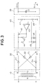
- the regulated power supply circuit is constituted by a transformer 10, a full-wave rectifying circuit 20, a voltage smoothing circuit 30 and a regulator circuit 40.
- V maximum amplitude voltage of ⁇ 24 Volts
- FIG. 2A is generated at the secondary winding of the transformer 10, and supplied to input terminals A(+) and B(-) of the full-wave rectifying circuit 20.
- Four diodes 21 through 24 are connected to the full-wave rectifying circuit 20.
- a load capacitor 31
- the ac signal shown in Fig. 2A is rectified and a full-wave rectified voltage consisting only of waveform portions of the positive polarity as illustrated in Fig. 2B is produced.
- A(+) terminal one of the output terminals is referred to as A(+) terminal
- B(-) (ground) terminal one of the output terminals.
- the smoothing circuit 30 made of the capacitor 31 is connected across the A(+) and B(-) terminals of the full-wave rectifier circuit 20, the the capacitor 31 is charged by the full-wave rectified voltage, and a discharge of the capacitor 31 takes place by the load such as the regulator circuit 40, so that a dc voltage including an amplitude fluctuation as shown in Fig. 2C will be generated.
- the dc voltage shown in Fig. 2C is supplied to the regulator circuit 40 of the next stage.
- the source of a P-channel MOS FET 41 (hereinafter abbreviated as FET) is connected at an A(+) terminal of the regulator circuit 40, and the drain of the FET 41 is connected to a C(+) terminal of the regulator circuit 40 which functions as its output terminal.
- a bias resistor 42 is connected across the source and gate of the EFT 41, and the gate is connected to an output terminal of an operational amplifier 43.
- a Zener diode 45 and a capacitor 46 are connected in parallel. Since a bias current from the source of the FET 41 is supplied to the cathode of the Zener diode 45 through a resistor 44, a stable breakdown voltage of the Zener diode 45 is supplied to the inverting input terminal of the operational amplifier 43 as a reference voltage of 6 V.
- the non-inverting input terminal of the operational amplifier 43 is connected to a node between a resistors 47 and 48 which are connected across the drain of the FET 41 and the ground terminal.
- the dc voltage having the amplitude fluctuation generated at the A(+) terminal of the full-wave rectifier circuit 20 (shown in Fig. 2C and its voltage level is assumed to be around 24 V) is supplied to the source terminal of the FET 41. Since the resistor 42 is connected across its source and gate, the FET 41 is put in an OFF (shut-off) state, so that the voltage at its drain is 0 Volt.
- the voltage applied at the source of the FET 41 flows into the Zener diode 45 through the resistor 44, the voltage of 6 V, that is the breakdown voltage of the Zener diode 45, is produced and supplied to the inverting input terminal of the operational amplifier 43.
- the voltage at the non-inverting input terminal (+) of the operational amplifier 43 which is supplied from the node between the resistors 47 and 48 connected across the drain and the ground terminal, is equal to 0 Volt because the voltage at the drain is 0 Volt.
- the voltage at the output terminal of the operational amplifier 43 temporarily assumes a low level (almost 0 Volt), and lowers the voltage at the gate of the FET 41 towards 0 Volt.
- the voltage at the gate of the FET 41 becomes lower than the voltage at its source, so that the FET 41 is put in an ON (conductive) state.
- a rising voltage shown in Fig. 2C is issued at the drain.
- the voltage developed at the drain is divided by the resistors 47 and 48, and in turn supplied to the non-inverting input terminal (+) of the operational amplifier 43.
- the resistance values of the resistors 47 and 48 are made equal to each other, almost a half of the voltage produced at the drain is supplied to the non-inverting input terminal of the operational amplifier 43.
- the reference voltage of 6 V is supplied to the inverting input terminal (-) of the operational amplifier 43.
- the operational amplifier 43 Since the operational amplifier 43 operates to multiply a voltage corresponding the difference between voltages at its non-inverting input terminal (+) and inverting input terminal (-) by a value corresponding to its gain, the output electric potential of the operational amplifier 43 changes to a high voltage.
- the control system of the regulator circuit 40 which is constituted by the output terminal of the operational amplifier 43, the gate and the drain of the FET 43, and the non-inverting input terminal of the operational amplifier 43, is made stable when the voltage of almost 6 V is supplied to the non-inverting input terminal (+) of the operational amplifier 43, in other words, when the electric potential at the drain has assumed almost 12 V.
- the regulated power supply circuit functions as a circuit for converting an ac signal to a dc signal, and obtaining a substantially constant dc voltage against the fluctuation of the ac signal.
- the electric power consumption of the FET used in the regulator circuit 40 can be calculated by multiplying a voltage corresponding to the difference between the voltages at the source and the drain (the area P 1 indicated by oblique lines in Fig. 2E) by the drain current (load current).
- the electric power consumption of the FET constitutes a substantial part of the electric power consumption of the regulator circuit 40, it is necessary to provide the FET 41 with a radiator of large size. Furthermore, although it is necessary that the voltage between its source and drain be set at a low level in order to reduce the electric power consumption of the FET 41, it will lead to a loss of freedom in designing especially in such cases that regulator circuit is used in an equipment for which the ac voltage being supplied or the dc voltage to be produced is minutely specified.
- the present invention has been made to solve the problem described above, and an object of the present invention is therefore to provide a regulated power supply circuit which is small in size but has a high efficiency, and with which a cost reduction can be achieved.
- the regulated power supply circuit comprises a rectifier circuit which rectifies an input alternating current (ac) voltage and converts the ac voltage to a rectified voltage, a voltage control circuit which receives the rectified voltage and performs a control operation to prevent a production of a voltage higher than a predetermined voltage, and a smoothing circuit for smoothing an output voltage of said voltage control circuit.
- ac alternating current
- the voltage control circuit which performs a control operation to prevent an output of a voltage higher than a predetermined voltage, is connected to the rectifier circuit which rectifies a supplied ac voltage and converts it to a rectified voltage, and the voltage smoothing circuit is provided on the output side of the voltage control circuit.
- Fig. 3 is a block diagram showing an embodiment of the regulated power supply circuit according to the present invention.
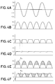
- the waveforms of voltages at various parts of the regulated power supply circuit are shown in Figs. 4A through 4F, respectively.
- an ac signal is converted in voltage by the primary and secondary windings of the transformer 10 and is, in turn, supplied to a full-wave rectifier circuit 20.
- the ac signal supplied from the secondary winding of the transformer 10 is processed as follows. As shown in Fig. 4A where it is assumed that its maximum amplitude voltages are ⁇ 24 V for example, half-wave components, on the positive polarity side, of the ac signal supplied to the full-wave rectifier circuit 20 are supplied to its A(+) terminal.
- the full-wave rectified voltage at the A(+) terminal is directly supplied to the source of the FET 41 of the regulator circuit 40. Since the resistor 42 is connected across the source and gate of the FET 41, the voltages at the source and gate are made equal, so that the FET 41 is put in an OFF (shut-off) state. In this state, the voltage at the drain is 0 Volt.
- the full-wave rectified voltage at the A(+) terminal is supplied to the Zener diode 45 through the resistor 44, and the voltage at the Zener diode 45 is fixed at +6 V by its breakdown voltage.
- This voltage is further smoothed out by the capacitor 46, and supplied to the inverting input terminal of the operational amplifier 43 as a dc reference voltage of +6 V. Since the dc reference voltage of +6 V is supplied to the inverting input terminal of the operational amplifier 43 and the voltage at its non-inverting input terminal is 0 Volt, the output voltage of the operational amplifier 43 drops temporarily, and draws the gate of the FET 41 to a low voltage side. As a result, the FET 41 is turned to an ON state (made conductive), and a voltage is supplied to its drain. The voltage at the drain is divided by the resistors 47 and 48, and in turn supplied to the no-inverting input terminal (+) of the operational amplifier 43.
- the operational amplifier 43 having two input terminals amplifies the difference voltage between the voltages at the two terminals at a gain factor that the operational amplifier 43 has.
- the output voltage of the operational amplifier 43 is produced on a low-voltage (almost 0V) side.
- the output voltage of the operational amplifier 43 is produced on a high-voltage (almost 24V) side.
- the inverting input terminal (-) is fixed to the reference voltage of 6V
- the voltage supplied to the drain of the FET 41 is divided by the resistors 47 and 48, and the above described operations are repeated until the voltage at the non-inverting input terminal (+) of the operational amplifier 43 reaches almost 6V.
- the waveform of the voltage shown in Fig. 4D includes a small fluctuation, the amount of fluctuation will be made small by using a capacitor of a sufficiently large capacity as the capacitor 31. Therefore this voltage can be regarded substantially as a dc voltage.
- the regulated power supply circuit according to the present invention can be adequately used for various circuits.
- the source voltage of the FET 41 existing when the regulator circuit 40 is operating properly is a full-wave rectified voltage of +24 V, and the drain voltage in that state is a dc voltage of +12 V.
- the electric power consumption of the FET 41 is a product of the voltage between the source and drain and the drain current, it is represented as the areas (P 2 ) indicated by the oblique lines in Fig. 4E.
- control circuit of the regulator circuit 40 is explained by way of an example which uses the P-channel MOS FET and an operational amplifier, it is also possible to use an N-channel MOS FET instead of the P-channel MOS FET, and an amplifier of other type can be used instead of the operational amplifier.
- circuit of the present invention may be used with a half-wave rectifier circuit instead of the full-wave rectifier circuit explained in the foregoing description. It also needless to mention that the same effect can be attained when a rectifier circuit having a configuration that a tap provided in the secondary winding of the transformer is used for the rectifying operation.
- the a voltage control circuit which presents the production of a voltage higher than a predetermined voltage is connected to a rectifier circuit which rectifies a supplied ac voltage and converts it to a rectified voltage, and the voltage smoothing circuit is connected to the output of the voltage control circuit.
- the head radiators for the parts of the voltage control circuit can be made small and light in weight.
- capacitors having a lower dielectric strength can be used in the voltage smoothing circuit. In this way, the regulated power supply circuit can be made small in size and made by using parts of small sizes and low prices, and the volume of the transformer can also be made small.
Landscapes
- Engineering & Computer Science (AREA)
- Physics & Mathematics (AREA)
- Electromagnetism (AREA)
- General Physics & Mathematics (AREA)
- Radar, Positioning & Navigation (AREA)
- Automation & Control Theory (AREA)
- Continuous-Control Power Sources That Use Transistors (AREA)
- Rectifiers (AREA)
Applications Claiming Priority (2)
| Application Number | Priority Date | Filing Date | Title |
|---|---|---|---|
| JP8166814A JPH09325825A (ja) | 1996-06-06 | 1996-06-06 | 電圧平滑化回路 |
| JP166814/96 | 1996-06-06 |
Publications (2)
| Publication Number | Publication Date |
|---|---|
| EP0811901A2 true EP0811901A2 (de) | 1997-12-10 |
| EP0811901A3 EP0811901A3 (de) | 1998-11-04 |
Family
ID=15838165
Family Applications (1)
| Application Number | Title | Priority Date | Filing Date |
|---|---|---|---|
| EP97109156A Withdrawn EP0811901A3 (de) | 1996-06-06 | 1997-06-05 | Spannungsgleichrichtungs- und Dämpfungsschaltung |
Country Status (3)
| Country | Link |
|---|---|
| US (1) | US5933337A (de) |
| EP (1) | EP0811901A3 (de) |
| JP (1) | JPH09325825A (de) |
Cited By (4)
| Publication number | Priority date | Publication date | Assignee | Title |
|---|---|---|---|---|
| EP0943974A1 (de) * | 1998-03-20 | 1999-09-22 | Endress + Hauser GmbH + Co. | Spannungsregelschaltung |
| FR2783942A1 (fr) * | 1998-09-30 | 2000-03-31 | St Microelectronics Sa | Dispositif de regulation de tension |
| WO2006087275A3 (de) * | 2005-02-17 | 2006-11-30 | Siemens Ag | Netzteil zur erzeugung einer niedrigen gleichspannung |
| US7199562B2 (en) | 2002-04-04 | 2007-04-03 | Thomson Licensing | Line frequency switching regulator |
Families Citing this family (3)
| Publication number | Priority date | Publication date | Assignee | Title |
|---|---|---|---|---|
| US6137276A (en) * | 1999-02-22 | 2000-10-24 | Mitel, Inc. | Onhook telecom power supply regulator mode |
| JP5352372B2 (ja) * | 2009-08-03 | 2013-11-27 | サクサ株式会社 | Ac/dc電源装置 |
| US9722498B2 (en) * | 2013-01-10 | 2017-08-01 | Alcatel Lucent | Control circuit for switching power converters with synchronous rectifiers |
Family Cites Families (8)
| Publication number | Priority date | Publication date | Assignee | Title |
|---|---|---|---|---|
| JPS57103521A (en) * | 1980-12-19 | 1982-06-28 | Iwatsu Electric Co Ltd | Power supply circuit |
| DE3501519A1 (de) * | 1985-01-18 | 1986-08-28 | BIOTEC Biotechnische-Apparatebau-Gesellschaft mbH, 4040 Neuss | Elektronische einrichtung zur reduktion der verlustleistung bei der erzeugung einer stabilisierten gleichspannung oder eines stabilisierten gleichstromes aus einer wechselspannungsquelle |
| US4943902A (en) * | 1987-11-23 | 1990-07-24 | Viteq Corporation | AC to DC power converter and method with integrated line current control for improving power factor |
| US4814687A (en) * | 1988-01-21 | 1989-03-21 | Honeywell, Inc. | Following voltage/current regulator |
| DE3907410C1 (de) * | 1989-03-08 | 1990-10-04 | Ant Nachrichtentechnik Gmbh, 7150 Backnang, De | |
| US5191278A (en) * | 1991-10-23 | 1993-03-02 | International Business Machines Corporation | High bandwidth low dropout linear regulator |
| DE4240264C2 (de) * | 1992-12-01 | 1995-01-26 | Legrand Gmbh | Netzteil |
| US5469046A (en) * | 1993-04-30 | 1995-11-21 | North American Philips Corporation | Transformerless low voltage switching power supply |
-
1996
- 1996-06-06 JP JP8166814A patent/JPH09325825A/ja active Pending
-
1997
- 1997-06-03 US US08/868,033 patent/US5933337A/en not_active Expired - Fee Related
- 1997-06-05 EP EP97109156A patent/EP0811901A3/de not_active Withdrawn
Cited By (6)
| Publication number | Priority date | Publication date | Assignee | Title |
|---|---|---|---|---|
| EP0943974A1 (de) * | 1998-03-20 | 1999-09-22 | Endress + Hauser GmbH + Co. | Spannungsregelschaltung |
| US6094040A (en) * | 1998-03-20 | 2000-07-25 | Endress + Hauser Gmbh + Co. | Voltage regulator circuit |
| FR2783942A1 (fr) * | 1998-09-30 | 2000-03-31 | St Microelectronics Sa | Dispositif de regulation de tension |
| US6218819B1 (en) | 1998-09-30 | 2001-04-17 | Stmicroelectronics S.A. | Voltage regulation device having a differential amplifier coupled to a switching transistor |
| US7199562B2 (en) | 2002-04-04 | 2007-04-03 | Thomson Licensing | Line frequency switching regulator |
| WO2006087275A3 (de) * | 2005-02-17 | 2006-11-30 | Siemens Ag | Netzteil zur erzeugung einer niedrigen gleichspannung |
Also Published As
| Publication number | Publication date |
|---|---|
| JPH09325825A (ja) | 1997-12-16 |
| EP0811901A3 (de) | 1998-11-04 |
| US5933337A (en) | 1999-08-03 |
Similar Documents
| Publication | Publication Date | Title |
|---|---|---|
| US5398182A (en) | Power supply | |
| EP0505982A1 (de) | Abschaltender Regler | |
| AU696737B2 (en) | High efficiency voltage converter and regulator circuit | |
| US4760322A (en) | Power-supply/battery back-up power supply/battery charger combination | |
| EP0811901A2 (de) | Spannungsgleichrichtungs- und Dämpfungsschaltung | |
| US8456872B2 (en) | Switching power supply | |
| US6583998B2 (en) | Power supply regulating having novel charging circuitry | |
| US4435747A (en) | High voltage supply system for medical equipment | |
| JPH09191638A (ja) | Dc/dcコンバータ | |
| JP3282309B2 (ja) | 電源装置 | |
| EP0589204A2 (de) | Verbesserung einer spannungsstabilisierten Stromversorgungsschaltung für einen Verstärkerwandler | |
| JPH06335176A (ja) | 充放電電源装置 | |
| KR960010372Y1 (ko) | 배터리 충전회로 | |
| JP2736059B2 (ja) | インバータ装置 | |
| JPH0418021Y2 (de) | ||
| KR100234753B1 (ko) | 저전력 스탠바이 회로 | |
| JPS60187260A (ja) | 自励発振式スイツチング電源装置 | |
| KR940001193Y1 (ko) | 정전압기의 발열 감쇄회로 | |
| JP3456803B2 (ja) | スイッチング電源 | |
| KR950010034Y1 (ko) | 노이즈 전압 감쇄회로 | |
| JPS591424Y2 (ja) | 電源電圧の監視方式 | |
| JP2003061349A (ja) | 電源のダミー回路 | |
| JPH03143260A (ja) | 直流安定化電源装置 | |
| JPS58151873A (ja) | 高圧電源装置 | |
| JPH0586130B2 (de) |
Legal Events
| Date | Code | Title | Description |
|---|---|---|---|
| PUAI | Public reference made under article 153(3) epc to a published international application that has entered the european phase |
Free format text: ORIGINAL CODE: 0009012 |
|
| AK | Designated contracting states |
Kind code of ref document: A2 Designated state(s): DE FR GB |
|
| PUAL | Search report despatched |
Free format text: ORIGINAL CODE: 0009013 |
|
| AK | Designated contracting states |
Kind code of ref document: A3 Designated state(s): DE FR GB |
|
| 17P | Request for examination filed |
Effective date: 19981104 |
|
| AKX | Designation fees paid |
Free format text: DE FR GB |
|
| 17Q | First examination report despatched |
Effective date: 20011217 |
|
| STAA | Information on the status of an ep patent application or granted ep patent |
Free format text: STATUS: THE APPLICATION IS DEEMED TO BE WITHDRAWN |
|
| 18D | Application deemed to be withdrawn |
Effective date: 20020430 |