EP0811916A2 - Maschenverbundene Matrize in einem fehlertoleranten Computersystem - Google Patents
Maschenverbundene Matrize in einem fehlertoleranten Computersystem Download PDFInfo
- Publication number
- EP0811916A2 EP0811916A2 EP97201662A EP97201662A EP0811916A2 EP 0811916 A2 EP0811916 A2 EP 0811916A2 EP 97201662 A EP97201662 A EP 97201662A EP 97201662 A EP97201662 A EP 97201662A EP 0811916 A2 EP0811916 A2 EP 0811916A2
- Authority
- EP
- European Patent Office
- Prior art keywords
- error
- bus
- biu
- data
- transaction
- Prior art date
- Legal status (The legal status is an assumption and is not a legal conclusion. Google has not performed a legal analysis and makes no representation as to the accuracy of the status listed.)
- Granted
Links
Images














Classifications
-
- G—PHYSICS
- G06—COMPUTING OR CALCULATING; COUNTING
- G06F—ELECTRIC DIGITAL DATA PROCESSING
- G06F11/00—Error detection; Error correction; Monitoring
- G06F11/07—Responding to the occurrence of a fault, e.g. fault tolerance
- G06F11/16—Error detection or correction of the data by redundancy in hardware
- G06F11/18—Error detection or correction of the data by redundancy in hardware using passive fault-masking of the redundant circuits
- G06F11/181—Eliminating the failing redundant component
-
- G—PHYSICS
- G06—COMPUTING OR CALCULATING; COUNTING
- G06F—ELECTRIC DIGITAL DATA PROCESSING
- G06F11/00—Error detection; Error correction; Monitoring
- G06F11/07—Responding to the occurrence of a fault, e.g. fault tolerance
- G06F11/16—Error detection or correction of the data by redundancy in hardware
- G06F11/1608—Error detection by comparing the output signals of redundant hardware
- G06F11/1625—Error detection by comparing the output signals of redundant hardware in communications, e.g. transmission, interfaces
-
- G—PHYSICS
- G06—COMPUTING OR CALCULATING; COUNTING
- G06F—ELECTRIC DIGITAL DATA PROCESSING
- G06F11/00—Error detection; Error correction; Monitoring
- G06F11/07—Responding to the occurrence of a fault, e.g. fault tolerance
- G06F11/16—Error detection or correction of the data by redundancy in hardware
- G06F11/1666—Error detection or correction of the data by redundancy in hardware where the redundant component is memory or memory area
-
- G—PHYSICS
- G06—COMPUTING OR CALCULATING; COUNTING
- G06F—ELECTRIC DIGITAL DATA PROCESSING
- G06F11/00—Error detection; Error correction; Monitoring
- G06F11/07—Responding to the occurrence of a fault, e.g. fault tolerance
- G06F11/16—Error detection or correction of the data by redundancy in hardware
- G06F11/18—Error detection or correction of the data by redundancy in hardware using passive fault-masking of the redundant circuits
-
- G—PHYSICS
- G06—COMPUTING OR CALCULATING; COUNTING
- G06F—ELECTRIC DIGITAL DATA PROCESSING
- G06F11/00—Error detection; Error correction; Monitoring
- G06F11/07—Responding to the occurrence of a fault, e.g. fault tolerance
- G06F11/16—Error detection or correction of the data by redundancy in hardware
- G06F11/18—Error detection or correction of the data by redundancy in hardware using passive fault-masking of the redundant circuits
- G06F11/182—Error detection or correction of the data by redundancy in hardware using passive fault-masking of the redundant circuits based on mutual exchange of the output between redundant processing components
-
- G—PHYSICS
- G06—COMPUTING OR CALCULATING; COUNTING
- G06F—ELECTRIC DIGITAL DATA PROCESSING
- G06F11/00—Error detection; Error correction; Monitoring
- G06F11/07—Responding to the occurrence of a fault, e.g. fault tolerance
- G06F11/16—Error detection or correction of the data by redundancy in hardware
- G06F11/18—Error detection or correction of the data by redundancy in hardware using passive fault-masking of the redundant circuits
- G06F11/187—Voting techniques
Definitions
- the present invention generally relates to a fault-tolerant computer system and, more particularly, to improved fault identification and reconfiguration performed in a mesh array computer architecture.
- Fault-tolerant computing is the art of building computing systems that continue to operate satisfactorily in the presence of faults (i.e. hardware or software failures).
- large commercial aircraft typically include complex flight control computer systems.
- the avionics systems of such aircraft can include three or more redundant computer systems. The systems process the same data from a common source or redundant data from different sources monitoring the same parameter. Should a fault cause an error in the output of one of the redundant computer systems, the outputs of the other systems that agree are used by the avionics system.
- the step of selecting data for use in a process from among the outputs of redundant sources is called "voting," which is a form of fault masking because the erroneous component is ignored.
- fault-tolerant systems can be configured to lock out one of the redundant channels if it continues to produce results that differ from the other channels. Reconfiguring a fault-tolerant system in this manner is a form of dynamic recovery. In another dynamic recovery procedure faulty modules are identified and switched out of the system and are substituted with a system spare. Thereafter, the system instigates roll back, initialization, retry, or restart actions necessary to continue ongoing computations.
- the mesh interconnected array is a matrix of nodes connecting identical central processing units (CPUs) to identical memory modules. This approach can be represented as multiple identical CPUs horizontally disposed with a CPU bus extending vertically below each CPU. Multiple identical memory modules are vertically disposed with memory buses extending horizontally to intersect the CPU buses at nodes or bus interface units (BIUs).
- BIUs bus interface units
- Existing mesh architectures perform fault masking and dynamic recovery by comparing pairs of BIUs.
- One BIU acts as a voting master and another as a voting checker. The checker is compared with the master and does not actively pass data.
- the present invention provides a reliable mesh interconnected array in a fault-tolerant computer system.
- the system includes multiple central processing units (CPUs), multiple memory units, and bus interface units (BIUs).
- the BIUs are located at the intersections of multiple vertical CPU buses and multiple horizontal memory buses. The result is a matrix of BIUs.
- Each BIU contains a transaction controller for transmitting a transaction including at least one of the following: address data, read data, write data, or control data.
- a mesh bus connects all BIUs within a single array of BIUs.
- the BIUs comprise an error detector for detecting correctable, retryable and non-retryable errors in the transmitted data of a transaction. An error corrector in each BIU corrects any correctable errors detected.
- a mesh error reporter in each BIU asserts to all the BIUs via the mesh bus if a retryable or non-retryable error was detected by the error detector.
- a retry mechanism sends the data back to the error detector a preset number of times if a retryable error remains asserted on the mesh bits.
- a fault manager isolates and eliminates BIUs with detected errors remaining after operation of the retry mechanism by reconfiguring the active status of each BIU connected on the mesh bus according to the type of remaining detected error(s).
- a continuation mechanism completes the transaction, if no error(s) remain asserted on the mesh bus.
- the error detector further comprises a single thread read back mechanism for detecting errors of data written to memory when only a single BIU or a single CPU channel is active.
- the fault manager within each BIU detects any self-implicating errors, shuts down each BIU that detects an uncorrectable self-implicating error, asserts a message to the mesh bus indicating the functioning status (active or inactive) of each BIU, and reconfigures the status of the BIUs by performing a configuration consistency algorithm.
- the fault management processor within each BIU detects any synchronization errors, asserts a first error message to the mesh bits if a synchronization error was detected, performs a first reconfiguration algorithm if a first error message was asserted on the mesh bus and performs the configuration consistency algorithm.
- the fault management processor within each BIU detects any memory bus errors, asserts a second error message to the mesh bus if a memory bits error was detected, performs a second reconfiguration algorithm if a second error message was asserted on the mesh bus and performs the configuration consistency algorithm.
- the fault management processor within each BIU detects any CPU bus errors, asserts a third error message to the mesh bus if a CPU hits error was detected, performs a third reconfiguration algorithm if a third error message was asserted on the mesh bus and performs the configuration consistency algorithm.
- the system includes as minimum architecture a CPU, at least one memory unit, and a BIU.
- the system of the present invention preferably includes multiple CPUs, multiple memory units, and multiple BIUs for greater tolerance of faults.
- the invention provides for fault identification and reconfiguration in a mesh array architecture that allows for single channel operation.
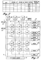
- FIGURE 1 is a block diagram of a plurality of bus interface units (BIU) 54 at nodes of a fault tolerant matrix (FTM) array in accordance with a preferred embodiment of the present invention.
- BIU bus interface units
- FTM fault tolerant matrix
- Multiple redundant central processing units (CPUs) 56 have associated CPU buses 50 intersecting memory buses 51.
- the memory buses extend from redundant memory units 57.
- a 2 by 3 matrix consisting of two rows of memory units 57 and three columns of CPUs 56 is used.
- Each BIU 54 provides a connection or node between a CPU bus 50 and a memory bus 51, i.e., a connection is provided for each column CPU 56 to each row memory unit 57.
- Each BIU is identified first by the row number of the connected memory unit 57 and then by the column number of the connected CPU 56. All the BIUs 54 in a single FTM are interconnected by a mesh bits 52. As shown in FIGURE 2, the location of each BIU 54 has an associated vector bit position which is part of a configuration vector in reconfiguration processing, described in more detail below with reference to FIGURES 19 and 20.
- the present invention is capable of operating various configurations, such as a single CPU 56 connected through a single BIU 54 to a single memory unit 57.
- the present invention also operates effectively if a single CPU is used with multiple redundant memory units, or a single memory channel is used with multiple redundant CPUs.
- a single CPU channel is identified by a single CPU 56 and CPU bus 50 connected to at least one memory bits 51 with a corresponding memory unit 57.
- a single memory channel has a single memory bus 51 and memory unit 57 connected to at least one CPU 56.
- the system is also effective when disjoint BIUs 54 are present. BIUs 54 are disjoint when two or more BIUs 54 fail to occupy the same CPU bus 50 and memory bus 51.
- the present invention is capable of handling matrix arrays larger than that shown in FIGURE 1.
- a 2 by 3 matrix array is effective for showing the redundant capabilities of the present invention.
- larger matrix arrays provide diminishing improvements in fault tolerant capabilities.
- FIGURE 3 is a block diagram illustration of two FTM arrays operating from the same set of CPUs 56, but connected to distinct memory systems.
- a first 2 by 3 mesh, mesh A has two memory units 57 each consisting of an electrically erasable programmable read-only memory (EEPROM) 57a, a single port random access memory (SRAM) 57b and a dual port random access memory (DPRAM) 57c.
- the memory rows of a second 2 by 3 mesh B comprise only a SRAM 57d and DPRAM 57e.
- Mesh B performs distinct yet synchronous operations from the same CPUs 56 that are coupled by mesh A.
- the CPUs 56 can operate a greater variety of functions with two FTMs connected. However, synchronization between the FTMs is a concern during operation.
- the mesh configuration of the present invention can integrate with various types of memory and input/output (I/O).
- System data requirements dictate the memory and I/O requirements.
- One I/O system the present invention can integrate with is an aircraft system integrated modular avionics box, such as an ARINC 629 bus attached to the DPRAMs.
- the purpose of the present invention is to effectively deliver or retrieve data from memory in the presence of error(s).
- all the BIUs have assigned roles.
- Each row and column has a BIU assigned a master role and the rest of the BIU(s) of that row or column are assigned checker roles.
- the master BIU is the only BIU allowed to write data to memory in each memory channel.
- Each CPU channel has a master BIU for data transactions between the BIUs 54 and the CPUs 56.
- the checker BIUs are used to check the master BIUs for correctness. Only active BIUs participate in all checking or voting performed in the algorithms of the present invention. When the system is fully functioning, two important interrelated tasks are performed.
- the first task detects errors internal and external to every BIU in a FTM.
- the other task is that of reconfiguration of the BIU's status according to the error detection task results. Reconfiguration is performed by a series of algorithms, described below with reference to FIGURES 14 ⁇ 21.
- FIGURE 4 is a block diagram of the internal components of a bus interface unit 54 with corresponding bus connections.
- the bus interface unit 54 includes an address datapath 58, a data datapath 59 and a transaction controller 63 connected there between.
- An initialization controller 64 also is connected between the address datapath 58 and data datapath 59.
- a fault identification and reconfiguration (FDIR) datapath 62 interacts with the transaction controller 63 and the initialization controller 64, and an input/output (I/O) controller 61 interacts with all other components of the BIU.
- Each BIU 54 includes a dual state machine. As shown in FIGURE 4, each controller and circuit path 58, 59, 61-64 has dual identical circuitry as illustrated by the shadowed black boxes.
- the dual state machine includes the dual identical circuits.
- the dual state machine provides comparison checking of many of the processes performed within the bus interface unit 54.
- the address datapath 58 connects externally to CPU bus 50 (shown at the left) and memory bus 51 (shown at the right). Internally, the address datapath 58 is coupled to transaction controller 63, initialization controller 64, and the data datapath 59. The address datapath 58 receives address data from the CPU bits 50 via a CPU address bus 66 and communicates with the memory bus 51 via a memory address bus 67. The data datapath 59 is internally coupled to transaction controller 63, initialization controller 64 and address datapath 58 (represented by the bold line 70 at the center). The data datapath 59 externally communicates with CPU bus 50 via a CPU data bus 58 and memory bus 51 via a memory data bits 69.
- Transaction controller 63 receives control data from CPU bus 50 via a CPU control bus 72 and is internally connected to all of the BIU's internal components except the initialization controller 64.
- Initialization controller 64 has no direct external connections and is internally connected to all of the BIU's components except the transaction controller 63.
- I/O controller 61 communicates memory control data to and from memory bus 51 via a memory control bus 71 and communicates with the other BIUs in the FTM by the mesh bus 52. Internally, the I/O controller 61 is also connected to the FDIR datapath 62.
- Transaction controller 63 determines from CPU control data the transaction that the BIU 54 is to perform and commands each of the components to perform according to the determined transaction. Some examples of transactions are data reads from memory along bus 69, data writes to memory along bus 69, and address accesses of memory along bus 67.
- the address datapath 58 processes address transactions and the data datapath 59 processes all read and write data transactions.
- Transaction controller 63 also controls the synchronization of all the components within the BIU 54 thus ensuring efficient processing of all information passing in and through the BIU 54.
- Initialization controller 64 provides control of the BIU 54 during startup and any required instruction fetches required during startup.
- each BIU 54 within an FTM stores a word (configuration vector) that corresponds to a status value of each BIU within the FTM.
- the precise storage location is described below with reference to FIGURE 20.
- the configuration vector is a six-bit word, each bit representing the status of a BIU within the FTM.
- each BIU 54 has a position in the FTM. The position has a corresponding bit in the configuration vector. For example, if the configuration vector was 011101, the BIUs in vector bit position 0, bottom left of FIGURE 1, and vector bit position 4, top center of FIGURE 1, are considered non-operative because of the zeroes in those respective positions.
- the considered non-operative BIUs are restricted from FTM operations provided all the BIUs 54 agree with this configuration vector, see below with reference to FIGURES 19-22.
- the FDIR datapath 62 reconfigures the configuration vector upon identification of faults from the other components within the BIU 54, or according to a change in status of other BIUs received from the mesh bus 52. The reconfiguration algorithm is described below with reference to FIGURES 19 and 20.
- I/O controller 61 provides an interfacing controlling unit with memory bus 51, mesh bus 52 and the internal components connected to the I/O controller 61.
- Each BIU 54 in the FTM continuously detects errors of data the BIU 54 receives, processes, and transmits.
- Two types of detected errors are value errors and synchronization errors.
- a value error is an error in the data received, processed or transmitted by the BIU 54.
- a synchronization error arises from inconsistencies in synchronization between the components within a BIU 54, inconsistencies in synchronization between the BIUs within an FTM, and synchronization inconsistencies with a second FTM as shown in FIGURE 3. It can be appreciated by one of ordinary skill that any additional units interacting with a FTM must be checked for synchronicity.
- Performance of dual state machine comparisons, parity checks, complementary signal checks, transaction consistency comparisons, wraparound comparisons of signals sent off the BIU, clock phase comparisons and mesh votes provide continuous analysis for errors that may occur anywhere in a transaction. Also, the analysis for errors allows each BIU to perform self-implicating error evaluations, thus providing a FTM that can operate with only one active BIU.
- the BIUs 54 are preprogrammed to characterize value and synchronization errors in two ways.
- the errors are first characterized as a BIU self-implicating error, a synchronization consistency error, a memory bus error or a CPU bus error. This identification is later used by the fault management procedure for further isolating the errors (see FIGURE 11). Also the errors are evaluated as either correctable, retryable or non-retryable. The second evaluation greatly affects how the fault management procedure reacts to the discovered error (described in more detail below with reference to FIGURES 5 and 20).
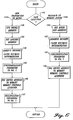
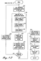
- FIGURES 5 ⁇ 13 illustrate the fault-tolerant process of a preferred embodiment of the present invention. All CPU memory transactions are processed through the BIUs 54 and are variations of reads to and writes from memory. As shown in FIGURE 5, each transaction received by a BIU 54 is analyzed for errors during phase operation, specifically an address phase and a data phase (110). FIGURES 6 and 8, described below, illustrate the error determining steps performed in the address and the data phases. If the error analysis determines that a retryable or non-retryable error is present in either of the phases, a message indicating so is asserted to the other BIUs via the mesh bus 52 (111) (non-retryable errors are described below with reference to FIGURE 11).
- the error analysis determines that the error present was correctable, the data is corrected (112). If no error was discovered during the phase analysis at 110, or if only correctable errors are present and are corrected at 112, the system proceeds to a decision 115. If at the decision 115 it is determined that no error is asserted on the mesh bus 52, the system proceeds to processing of the next transaction. If an error is asserted on the mesh bus 52, the system proceeds to the fault management procedure 116.
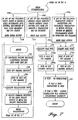
- FIGURE 6 illustrates the processing steps performed within the address phase of operation.
- a case selection 144 is performed on the data received in the address phase.
- Case selection 144 determines whether the data received is from a new transaction or a retry, branch 144a, or from a readback or a memory scrub, branch 144b.
- An address phase retry is performed in a retry procedure described below with reference to FIGURE 9, and the readback case is described below with reference to FIGURE 13.
- the memory scrub case performs correction of incorrectly stored information determined correctable during a read transaction.
- the CPU drives the address at 140 to the BIU which latches the address at 141. Then the address is decoded and a cache RAM hit/miss determination is performed at 142.
- cache in the address datapath 58 provides faster access to instructions/data stored in EEPROM.
- the address phase then performs a synchronization procedure at 145 and a nullification procedure at 147 (both procedures are illustrated in FIGURE 7 and described below).
- the BIU drives the address to memory and memory controls are asserted at 146 onto the memory control bus 71.
- the address phase analysis of the new transaction or retry, branch 144a is complete upon completion of the nullification procedure, thus returning any errors determined in the address phase procedure, synchronization procedure or nullification procedure.
- the address phase procedure selects the case of a readback or memory scrub, branch 144b, the address phase procedure performs all of the same tasks as the retry case except the BIU uses the previously held address (143) and the procedure does not perform the nullification procedure.
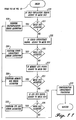
- FIGURE 7 illustrates the synchronization procedure at 145 of FIGURE 6 and the nullification procedure at 147 that operate within the address phase.
- the synchronization procedure performs three simultaneous functions shown as paths 169a, b and c.
- One function, 169a determines if a synchronization error occurs in the address phase of operation.
- the other two simultaneous functions, paths 169b and c drive a FTM address flag if the BIU thinks it is being addressed by the CPU and drives a mesh consistency signal if the BIU believes its address phase operation is consistent with the memory in memory units 57.
- the driven address flag is qualified with any driven error signals at 175, then passed to the algorithm beginning at 176a and 180a, described below with reference to FIGURE 16A.
- the driven consistency signal is similarly qualified with the error signals at 177 and processed through an algorithm at 176b and 180b, described below with reference to FIGURE 17A.
- resulting actions are performed on the analysis of data from the beginning of the synchronization process. If no flag signal exists, no transaction will be prosecuted. If an address and a transaction consistency signal exist, then the synchronization process indicates that the transaction is good. However, if a flag is present and no transaction consistency signal is present, the transaction is illegal and will generate a synchronous interrupt signal for further use in the fault management procedure.
- the nullification procedure is illustrated with the synchronization procedure, since it uses the same driven error output of 170.
- the CPU 56 pipelines transactions through BIUs 54 for efficient processing. However, situations may occur when a transaction in the pipeline is not necessary and must be nullified.
- the nullification procedure provides the FTM with the capabilities of nullifying an unwanted transaction. If a nullification signal is received by BIU, an output signal is sent to the mesh bus 52 to nullify the transaction at 190. The nullification signal sent to the mesh bus 52 is then qualified by the error signal output of 170 and execution of the nullification algorithm of 185 and 186 is executed.
- the other procedure performed in the error detection test at 110 of FIGURE 5 is the data phase procedure, shown in FIGURE 8.
- the data phase procedure includes case selection at 153 for choosing one of five transactions shown as paths 167a-e according to the data received by the data datapath 59: a read transaction 167a; a write transaction 167b; an interrupt transaction 167c; a scrub transaction 167d; a readback transaction 167e. If the case is a read transaction 167a, a data read from memory, the BIU latches the data read from memory at 150, checks it for errors in an error detecting and correcting circuit (EDAC) located within datapath 59 and generates parity at 152, and drives the data onto the CPU bus 50 at 156.
- EDAC error detecting and correcting circuit
- the BIU latches the data from the CPU to be written to memory at 151, generates error correcting code (ECC) at 155 and drives the data received from the CPU onto the memory bus at 157.
- the write transaction includes a step B that is described in more detail below with FIGURE 8B. If the transaction is an interrupt 167c, interrupt parameters are written to an interrupt register at 158. The interrupt transaction initiates from errors requiring the FTM and/or BIU to temporarily stop processing. If the case is a scrub transaction 167d, error correcting code (ECC) is generated at 162 and the BIU drives the data to be stored onto the memory bits and asserts memory controls at 161.
- ECC error correcting code
- the memory controls are asserted 163, the BIU latches the data sent to memory at 166, checks the stored data by EDAC and compares that data to the received data from the CPU at 165.
- the scrub transaction performs corrections of correctable data. Completion of each of the cases within the data phase procedure returns the procedure back to the decision on page 17 at 110 of FIGURE 5 with any errors determined by the data se procedure.
- a check is performed on the memory stored data of a write transaction during either single CPU channel or single memory channel writing to DPRAM at 127. If the data written to memory is correct, the process returns to phase processing 110 of FIGURE 5. If the data is incorrect but correctable (131), the data is corrected (132). However, if the data is incorrect but not correctable, an error is asserted on the mesh bus.
- the fault management procedure 116 is initiated, as shown in FIGURES 9 ⁇ 12.
- the process moves directly to a fault identification and reconfiguration (FDIR) procedure 208, if a non-retryable error was previously discovered.
- FDIR fault identification and reconfiguration
- the system separately retries the address and data phase procedures at 197-205.
- address phase procedure errors are latched and saved until completion of the data phase procedure. This allows the next transaction to start the address phase procedure when the present transaction starts the data phase procedure.
- a preset number of retries are performed until no errors are asserted on the mesh bus 52, as determined by a decision at 205, or the retry limit is reached, as determined by decision 207. If the retry purges the retryable error(s), the system proceeds to processing the next transaction. If a fault is still asserted on the mesh bus 52 after reaching the retry limit, the system proceeds to the FDIR procedure 208.
- the FDIR procedure 208 first checks for address phase errors at 210-212, then data phase errors at 215-217. If an error is detected in either of the phases at 212 and 217, the fault identification (FID) procedure 218 is separately initiated. Essentially at this,stage of the procedure any errors present are categorized into one of the two phases, address or data. The FID procedure 218 further isolates any errors, within each phase and reconfigures the mesh configuration vector according to any detected errors.
- FID fault identification
- FIGURE 11 illustrates the FID procedure 218 that further isolates any errors and reconfigures the configuration vector according to the location of the error(s).
- Each BIU maintains the n bit configuration vector that indicates the BIU perception of the status of each of the n BIUs in the FTM.
- n 6 because there are six BIUs in the 2 by 3 matrix array.
- the first analysis determines if the error(s) are characterized as self-implicating at 220. If one or more self-implicating errors exist, an error message is asserted on the mesh bus 52 from a decision at 221. All BIUs continuously send a phased heartbeat signal to the BIUs via the mesh bus 52.
- the heartbeat signal is continually cycling at a particular cycling phase known to all the BIUs. If the heartbeat signal of a BIU is received out of phase, the BIU is killed or removed from voting. A non-retryable error is an error that causes an erroneous change in the BIU's heartbeat signal.
- the self-implicated BIU shuts down at 223 and sends a change of its phased heartbeat signal to all the BIUs in the FTM.
- a phase changed heartbeat signal indicates that the configuration vector will require and must undergo reconfiguration.
- the individual BIU reaction to a changed heartbeat signal is described below with reference to FIGURE 20.
- a configuration consistency procedure 237 performs any necessary reconfiguration of the configuration vector.
- the configuration consistency procedure performs a configuration voting algorithm (CVA) and reassigns the master BIUs accordingly, described below with reference to FIGURES 19 ⁇ 22.
- CVA configuration voting algorithm
- the system returns to the FDIR procedure 208 (FIGURE 10) to continue checking for any other errors of the same phase (address or data).
- the three other error types are isolated through separate processing passes in the FID procedure. Synchronization consistency errors, memory bus errors, and CPU bus errors are isolated and reconfigured according to predefined algorithms. The synchronous consistency algorithms are described below with reference to FIGURES 18A and 19A. The reconfiguration algorithm for memory bus errors is described below with reference to FIGURE 14A. The CPU bus error algorithm is described below with reference to FIGURE 15A. After an error is purged by the corresponding algorithm, the configuration consistency procedure (FIGURE 12) performs any necessary reconfiguration followed by a return to the FDIR procedure, for further error processing.
- each BIU receives, at 240, the configuration vector from all the other BIUs.
- the CVA then performs a comparison of each bit within the configuration vectors at 241, 242 and 245.
- First the BIUs in the memory channel vote on a bit in the configuration vector at 241, see below with reference to step 1 of FIGURE 19A.
- results of the memory channels' votes are voted on for each bit in the configuration vector at 242 and the BIUs voting dead of a determined active BIU is eliminated at 245, see below with reference to step 2 of FIGURE 19A.
- each BIU compiles a new consensus configuration vector at 246 and compares this to a prestored reference configuration vector at 247, see below with reference to FIGURE 19 and 20.
- the address phase and data phase procedures are performed prior to 110 of FIGURE 5 and during the fault management procedure (at 197, 201, 210 and 215 of FIGURES 9 and 10).
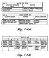
- FIGURE 14A illustrates the two step memory bus error algorithm performed at 230 of FIGURE 11.
- step 1 the memory channel master BIU rechecks for any self-implicating errors, column A.. Elimination of the master row 2, column B occurs if the master self-implicates. If the master does not self-implicate, step 2 initiates row 2, column A. Step 2 is a majority BIU agree or disagree vote of the data the respective channel master placed on the memory bus 51. If the majority decision of the BIUs agree with the memory bus data, the row 1, column A transaction proceeds, row 1, column B, and any disagreeing BIU is eliminated, row 2, column C.
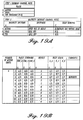
- FIGURE 14B enumerates some configurations and actions.
- column B from FIGURE 14B, the memory channel master does not self-implicate itself.
- the master and one other BIU in the same memory channel agree, rows 1, 2, and the last BIU in the same memory channel disagrees, row 3, with the data the master placed on the memory bus 51. The result is that the transaction proceeds and the disagreeing BIU is eliminated, row 4.
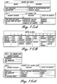
- FIGURE 15A illustrates the two step CPU bus error algorithm performed at 235 of FIGURE 11.
- Step 1 is similar to step 1 of the memory bus error algorithm of FIGURE 14A except the CPU channel's master BIU is the master BIU of interest.
- Step 2 is a strict majority vote of the data the master CPU channel BIU places on the CPU bus 50.
- Step 2 is similar to step 2 described in FIGURE 14A above.
- FIGURE 15B enumerates some configurations and corresponding actions. Column E is described below for an example.
- the CPU channel master BIU determines no self-implication exists. The CPU channel master BIU agrees with what it placed on the CPU bus 50, row . Only one other BIU is active in the same CPU channel and this BIU disagrees, row 2, with the data the master BIU placed on the CPU bus 50. With no majority result this CPU channel is eliminated, column 14, and no further transaction processing is performed by this CPU channel.
- faults indicated by errors relating to FTM addressing 176a, 180a of FIGURE 7 are resolved by a two step majority vote of the BIUs 54 in the FTM.
- step 1 the BIUs 54 on each of the CPU channels vote if they think the CPU 56 is addressing the FTM.
- step 2 the results from all of the CPU channel votes are voted. Ties in the first step are neutral to the outcome of the second step.
- Specific error information relating to the FTM address flag and the mesh consistency is placed on the mesh bus 52 to nullify the validity of the flag and mesh consistency of an otherwise active BIU. The results of most cases agree with that of a simple majority.
- the fault syndrome columns A, B, C represent the CPU columns and each of the two responses in a column represents a voting BIU on a separate memory channel.
- a tie is experienced by the addressing votes of the BIUs in coliimn A, B CPU channels and a consensus yes address vote of the two BIUs in the right CPU channel column C.
- the resulting majority CPU channel vote is yes, column D.
- the FTM is being addressed, the transaction is initiated and the BIUs that voted not addressed, top left and bottom center BIU, are eliminated, column E, F.
- the "Comments" columns for FIGURES 16-19 are reserved for comments regarding the corresponding row results.
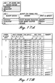
- FIGURE 17A The voting algorithm 176b, 180b of FIGURE 7 and 226 of FIGURE 11 is shown in FIGURE 17A.
- step 1 if the majority CPU channel vote decides that the transaction is inconsistent, row 2, then a memory exception is initiated in step 2, row 2.
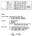
- FIGURES 17B-D enumerate the generic configurations and actions with an explanation on notation at the end of the table. The results of most cases agree with that of a simple majority. The exceptions are noted by "minority" and "tie breaker" in the Comment column. For the minority results, the results are more conservative than a simple majority vote.
- the nullification vote of 182, 185, 186 of FIGURE 7 differs from the previous two synchronization consistency error algorithms in that the vote takes place after the action has occurred.
- the decision to nullify or continue, column B of step 2 must be made by each BIU without the benefit of a synchronizing transaction on the mesh bus 52. Therefore, in order to maintain synchronization, a post-action vote is performed and the disagrees immediately shut down, column C, to avoid loss of synchronization, see step 2. This must be done because the nullification/continuation decision results in an irrevocable change of state in the system.
- Nullification occurs for three reasons: the CPUs 56 assert a nullification signal; the other FTM asserts a hold signal; or self-shutdown of a BIU. Only the first two cases are significant because the third case is self-resolving. A discrepancy in the nullification vote due to either nullification or hold signal assertion, implies either a data error or the loss of synchronization across the CPU channels.
- FIGURE 18A specifies the two-step fault identification process for the nullification mesh vote.
- the nullify decision is asserted onto the mesh bus 52 between counts of the clock.
- step 1 of FIGURE 18A the BIUs for each CPU channel are voted, generating votes for the CPU channels.
- step 2 all of the CPU channel votes from step 1 are voted. If a BIU 54 recognizes that its nullification decision did not match the decision of the mesh vote, then that BIU shuts down column C and broadcasts the shut clown by changing its heartbeat signal.
- the change in the BIU's heartbeat signal is an immediate indication to the FTM that a BIU has killed itself. Surviving BIUs detect the heartbeat change and perform the configuration consistency procedure to generate a new configuration vector.
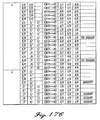
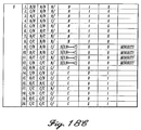
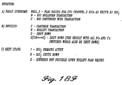
- FIGURES 18B-F enumerate some generic configurations and corresponding actions with an explanation on notation at the end of the table. For one example see the row 10 of FIGURE 18B.
- the left and center CPU channels, column A, B experience a tie of the included BIUs.
- the right CPU channel vote, column C is to continue, not nullifying the transaction.
- the combined vote of the CPU channels is to continue, column D.
- the BIUs voting to nullify the continued transaction above are eliminated, column E, because these BIUs disagree with the result.
- FIGURE 19A illustrates the CVA performed at 241, 242 and 245 of FIGURE 12.
- FIGURES 19B-E enumerate generic configurations and actions with a notation explanation.
- the CVA performs a memory channel vote on each vector bit of the configuration vectors generated by the BIUs 54.
- the memory channel votes are combined to form an intermediate result.
- column C is called "dead removal.” Dead removal refers to the marking as dead any BIU that voted the subject BIU dead in a vote in which the result had the subject BIU remaining active, row 1, column C. If the combination memory channel vote results in a majority dead decision, row 2, or a tie the BIU is eliminated, row 3.
- Row 10 of FIGURE 19B is one example of a result from the CVA. This particular vote is on the left upper-most BIU in the FTM.
- the result of step 1 is both memory channels voting the BIU dead. Thus, the resulting combined memory channels' vote is dead and therefore removal of the left most BIU, column D, E.
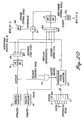
- FIGURE 20 illustrates the configuration consistency circuitry.
- the configuration consistency circuitry includes a StateIn register 92 that outputs data to a CVA circuit 93.
- the output of CVA circuit 93 passes through a multiplexer (MUX)98a to a new state register 91 and through a second MUX 98b to an old state register 90.
- CVA circuit output and an output of the new state register 91 is received by a StateMismatch comparator 94.
- Old state register 90 outputs directly to a opti generator 95 and through an AND gate 97 to a columnmaster generator 96. Changed heartbeat signals are also received by AND gate 97 and the output of AND gate 97 is received by the CVA circuit 93.
- the old state register 90 always stores the current configuration vector.
- a configuration is implemented by storing the configuration vector into the old state register 90.
- a killmask marks either a BIU that has a pending, non-retryable error, as signaled by a changed heartbeat signal, or any BIU whose heartbeat is not phased properly.
- the BIU performs the reconfiguration procedure and generates a new configuration vector, it stores that configuration vector in a new state register 91.
- the new state register 91 performs a circular shift of the 6 bit configuration vector, asserting it onto a StateOut line and ending the shift with the vector aligned again within the new state register 91.
- the StateOut line is passed to all BIUs 54 on the mesh bus 52 via a MUX 99a and reenters the circuit at the StateIn register 92.
- each BIU 54 receives at StateIn register 92 a copy of the configuration vectors that each BIU 54 in the FTM has generated and stored in the new state register 91.
- the CVA as defined previously in FIGURE 19A, is invoked and a new, composite configuration vector is generated from the data in the StateIn register 92 and any possible killed BIUs as received through AND gate 97. If the composite configuration vector matches the contents of the new state register 91, as determined at StateMismatch comparator 94, the process is complete and the new configuration is implemented.
- the new state register 91 is loaded through MUX 98a with a prestored configuration vector retrieved from the EEPROM and the configuration consistency procedure is invoked using that vector as an initial value. It is possible that the configuration vector retrieved by the BIUs of one memory channel does not match the vector retrieved by the BIUs of other memory channels. Consider the case in which an entire memory channel is shut down during operation. The EEPROM from that memory channel does not have the updated configuration vector stored into it because that channel can no longer respond to transactions. It contains a configuration vector that has some of the BIUs of the inactive channel marked as still active.
- all BIUs 54 start as active until shown otherwise.
- the previously deactivated memory channel is active until either individual checks or the configuration consistency procedure illustrate it to be inactive.
- the inactive status of the bad memory channel is determined if only one of the memory channels contains the accurate vector indicating that the bad channel should be inactive.
- the final vote of memory channels must be explicitly positive. A vote by either memory channel to kill a BIU results in the deactivation of that BIU. Therefore, consistency is maintained.
- the assignment of memory channel and CPU channel masters is determined as a function of the configuration vector.
- the Mastership status is determined from the old state register 90 contents which should be consistent.
- the algorithm for determining memory channel Mastership is shown in FIGURE 21. When the master memory channel BIU is deactivated, mastership assignment increments column position until an active BIU is reached. Memory channel mastership is simple because memory channel master assignments have priority over CPU channel master assignments.
- the rules for determining CPU channel mastership are more complicated because the CPU channel mastership may be passed from a still-active BIU to its column pair in order to avoid the situation in which a BIU is both memory channel and CPU channel master.
- the algorithm for determining CPU channel mastership is shown in FIGURE 22. Three possible cases exist if both BIUs in a CPU channel are active. In case 1 neither BIU is the memory channel master; therefore, the CPU channel master retains mastership. Case 2 has the same result when both BIUs are memory channel masters. In case 3 one BIU is a memory channel master and CPU mastership assignment goes to the nonmemory channel master. When a single BIU is active in the CPU channel, it is the master.
- the present invention provides improved fault identification and reconfiguration performed in a mesh array computer architecture because of a number of important factors previously described.
- This system's ability to categorize errors as to their type and location and to reconfigure the mesh architecture according to the identified errors, are two features that enable the improvements of this invention.
Landscapes
- Engineering & Computer Science (AREA)
- Theoretical Computer Science (AREA)
- Quality & Reliability (AREA)
- Physics & Mathematics (AREA)
- General Engineering & Computer Science (AREA)
- General Physics & Mathematics (AREA)
- Hardware Redundancy (AREA)
Applications Claiming Priority (2)
| Application Number | Priority Date | Filing Date | Title |
|---|---|---|---|
| US660601 | 1996-06-06 | ||
| US08/660,601 US5742753A (en) | 1996-06-06 | 1996-06-06 | Mesh interconnected array in a fault-tolerant computer system |
Publications (3)
| Publication Number | Publication Date |
|---|---|
| EP0811916A2 true EP0811916A2 (de) | 1997-12-10 |
| EP0811916A3 EP0811916A3 (de) | 1999-04-28 |
| EP0811916B1 EP0811916B1 (de) | 2003-04-02 |
Family
ID=24650189
Family Applications (1)
| Application Number | Title | Priority Date | Filing Date |
|---|---|---|---|
| EP97201662A Expired - Lifetime EP0811916B1 (de) | 1996-06-06 | 1997-06-06 | Maschenverbundene Matrize in einem fehlertoleranten Computersystem |
Country Status (4)
| Country | Link |
|---|---|
| US (1) | US5742753A (de) |
| EP (1) | EP0811916B1 (de) |
| CA (1) | CA2206840C (de) |
| DE (1) | DE69720322T2 (de) |
Cited By (11)
| Publication number | Priority date | Publication date | Assignee | Title |
|---|---|---|---|---|
| WO2001042936A3 (en) * | 1999-12-09 | 2001-12-27 | Rambus Inc | Transceiver with latency alignment circuitry |
| US7000062B2 (en) | 2000-01-05 | 2006-02-14 | Rambus Inc. | System and method featuring a controller device and a memory module that includes an integrated circuit buffer device and a plurality of integrated circuit memory devices |
| US7051151B2 (en) | 2000-01-05 | 2006-05-23 | Rambus Inc. | Integrated circuit buffer device |
| US7266634B2 (en) | 2000-01-05 | 2007-09-04 | Rambus Inc. | Configurable width buffered module having flyby elements |
| US7356639B2 (en) | 2000-01-05 | 2008-04-08 | Rambus Inc. | Configurable width buffered module having a bypass circuit |
| US7363422B2 (en) | 2000-01-05 | 2008-04-22 | Rambus Inc. | Configurable width buffered module |
| US7404032B2 (en) | 2000-01-05 | 2008-07-22 | Rambus Inc. | Configurable width buffered module having switch elements |
| US7464225B2 (en) | 2005-09-26 | 2008-12-09 | Rambus Inc. | Memory module including a plurality of integrated circuit memory devices and a plurality of buffer devices in a matrix topology |
| US7562271B2 (en) | 2005-09-26 | 2009-07-14 | Rambus Inc. | Memory system topologies including a buffer device and an integrated circuit memory device |
| GB2577120A (en) * | 2018-09-14 | 2020-03-18 | Ultrasoc Technologies Ltd | Error detection within an integrated circuit chip |
| US11328764B2 (en) | 2005-09-26 | 2022-05-10 | Rambus Inc. | Memory system topologies including a memory die stack |
Families Citing this family (33)
| Publication number | Priority date | Publication date | Assignee | Title |
|---|---|---|---|---|
| US6141769A (en) * | 1996-05-16 | 2000-10-31 | Resilience Corporation | Triple modular redundant computer system and associated method |
| JP2877095B2 (ja) * | 1996-08-28 | 1999-03-31 | 日本電気株式会社 | マルチプロセッサシステム |
| US6000040A (en) * | 1996-10-29 | 1999-12-07 | Compaq Computer Corporation | Method and apparatus for diagnosing fault states in a computer system |
| US5941997A (en) * | 1996-11-26 | 1999-08-24 | Play Incorporated | Current-based contention detection and handling system |
| US5903717A (en) * | 1997-04-02 | 1999-05-11 | General Dynamics Information Systems, Inc. | Fault tolerant computer system |
| US6138253A (en) * | 1997-05-29 | 2000-10-24 | Oracle Corporation | Method and apparatus for reporting errors in a computer system |
| US6334193B1 (en) * | 1997-05-29 | 2001-12-25 | Oracle Corporation | Method and apparatus for implementing user-definable error handling processes |
| US6035425A (en) * | 1997-09-29 | 2000-03-07 | Lsi Logic Corporation | Testing a peripheral bus for data transfer integrity by detecting corruption of transferred data |
| JPH11259383A (ja) * | 1998-03-12 | 1999-09-24 | Hitachi Ltd | Ras情報取得回路及びそれを備えた情報処理システム |
| US6286110B1 (en) * | 1998-07-30 | 2001-09-04 | Compaq Computer Corporation | Fault-tolerant transaction processing in a distributed system using explicit resource information for fault determination |
| US7061821B2 (en) * | 1998-10-20 | 2006-06-13 | International Business Machines Corporation | Address wrap function for addressable memory devices |
| US6411981B1 (en) | 1999-03-12 | 2002-06-25 | Compaq Computer Corporation | Method and apparatus for conducting a transaction between homogeneous and/or heterogeneous transaction processing systems using asynchronous pull of a transaction transfer |
| US7020076B1 (en) * | 1999-10-26 | 2006-03-28 | California Institute Of Technology | Fault-tolerant communication channel structures |
| US6996745B1 (en) * | 2001-09-27 | 2006-02-07 | Sun Microsystems, Inc. | Process for shutting down a CPU in a SMP configuration |
| US6848062B1 (en) | 2001-12-21 | 2005-01-25 | Ciena Corporation | Mesh protection service in a communications network |
| US20050002223A1 (en) * | 2002-02-06 | 2005-01-06 | Coteus Paul William | Output driver impedance control for addressable memory devices |
| US7185233B2 (en) * | 2002-05-14 | 2007-02-27 | Sun Microsystems, Inc. | Method and apparatus for inserting synchronized errors |
| US20040153748A1 (en) * | 2002-12-19 | 2004-08-05 | Alfio Fabrizi | Method for configuring a data processing system for fault tolerance |
| US7467326B2 (en) * | 2003-02-28 | 2008-12-16 | Maxwell Technologies, Inc. | Self-correcting computer |
| JP4774347B2 (ja) * | 2006-08-18 | 2011-09-14 | 富士通株式会社 | ノード装置、制御装置、制御方法及び制御プログラム |
| US8656392B2 (en) * | 2009-06-10 | 2014-02-18 | The Boeing Company | Consensus based distributed task execution |
| TWI410087B (zh) | 2010-12-20 | 2013-09-21 | Ind Tech Res Inst | 多核心晶片網路 |
| US8914165B2 (en) * | 2011-03-29 | 2014-12-16 | Hamilton Sundstrand Corporation | Integrated flight control and cockpit display system |
| US9256426B2 (en) | 2012-09-14 | 2016-02-09 | General Electric Company | Controlling total number of instructions executed to a desired number after iterations of monitoring for successively less number of instructions until a predetermined time period elapse |
| US9342358B2 (en) | 2012-09-14 | 2016-05-17 | General Electric Company | System and method for synchronizing processor instruction execution |
| US20140281678A1 (en) * | 2013-03-14 | 2014-09-18 | Kabushiki Kaisha Toshiba | Memory controller and memory system |
| US9710342B1 (en) | 2013-12-23 | 2017-07-18 | Google Inc. | Fault-tolerant mastership arbitration in a multi-master system |
| CN107168226A (zh) * | 2017-05-31 | 2017-09-15 | 宁波弘泰水利信息科技有限公司 | 一种闸泵自动化控制方法 |
| US11099748B1 (en) * | 2018-08-08 | 2021-08-24 | United States Of America As Represented By The Administrator Of Nasa | Fault tolerant memory card |
| TWI719741B (zh) | 2019-12-04 | 2021-02-21 | 財團法人工業技術研究院 | 改變冗餘處理節點的處理器及其方法 |
| CN113296531A (zh) * | 2021-05-19 | 2021-08-24 | 广东汇天航空航天科技有限公司 | 飞行控制系统、飞行控制方法和飞行器 |
| CN115577225B (zh) * | 2022-12-07 | 2023-05-12 | 通号万全信号设备有限公司 | 二取二表决处理方法、设备及存储介质 |
| EP4517531A1 (de) * | 2023-08-30 | 2025-03-05 | Siemens Mobility GmbH | Verfahren zum durchführen eines technischen prozesses im regelbetrieb und reparaturbetrieb |
Family Cites Families (13)
| Publication number | Priority date | Publication date | Assignee | Title |
|---|---|---|---|---|
| US4323966A (en) * | 1980-02-05 | 1982-04-06 | The Bendix Corporation | Operations controller for a fault-tolerant multiple computer system |
| US4493081A (en) * | 1981-06-26 | 1985-01-08 | Computer Automation, Inc. | Dynamic memory with error correction on refresh |
| US4438494A (en) * | 1981-08-25 | 1984-03-20 | Intel Corporation | Apparatus of fault-handling in a multiprocessing system |
| US4503534A (en) * | 1982-06-30 | 1985-03-05 | Intel Corporation | Apparatus for redundant operation of modules in a multiprocessing system |
| US4503535A (en) * | 1982-06-30 | 1985-03-05 | Intel Corporation | Apparatus for recovery from failures in a multiprocessing system |
| US4570261A (en) * | 1983-12-09 | 1986-02-11 | Motorola, Inc. | Distributed fault isolation and recovery system and method |
| US4589066A (en) * | 1984-05-31 | 1986-05-13 | General Electric Company | Fault tolerant, frame synchronization for multiple processor systems |
| US4697344A (en) * | 1986-05-23 | 1987-10-06 | The Cloverline Incorporated | Pill cutter |
| US4914657A (en) * | 1987-04-15 | 1990-04-03 | Allied-Signal Inc. | Operations controller for a fault tolerant multiple node processing system |
| US5212785A (en) * | 1990-04-06 | 1993-05-18 | Micro Technology, Inc. | Apparatus and method for controlling data flow between a computer and memory devices |
| US5048816A (en) * | 1990-07-09 | 1991-09-17 | Murata Wiedemann, Inc. | Workpiece registration system and method for determining the position of a sheet |
| JPH06275098A (ja) * | 1993-03-24 | 1994-09-30 | Mitsubishi Electric Corp | 半導体記憶装置 |
| GB9313255D0 (en) * | 1993-06-26 | 1993-08-11 | Int Computers Ltd | Fault-tolerant computer systmes |
-
1996
- 1996-06-06 US US08/660,601 patent/US5742753A/en not_active Expired - Lifetime
-
1997
- 1997-06-03 CA CA002206840A patent/CA2206840C/en not_active Expired - Lifetime
- 1997-06-06 DE DE69720322T patent/DE69720322T2/de not_active Expired - Lifetime
- 1997-06-06 EP EP97201662A patent/EP0811916B1/de not_active Expired - Lifetime
Cited By (41)
| Publication number | Priority date | Publication date | Assignee | Title |
|---|---|---|---|---|
| US7065622B2 (en) | 1999-12-09 | 2006-06-20 | Rambus Inc. | Transceiver with latency alignment circuitry |
| US6643752B1 (en) | 1999-12-09 | 2003-11-04 | Rambus Inc. | Transceiver with latency alignment circuitry |
| US8086812B2 (en) | 1999-12-09 | 2011-12-27 | Rambus Inc. | Transceiver with latency alignment circuitry |
| WO2001042936A3 (en) * | 1999-12-09 | 2001-12-27 | Rambus Inc | Transceiver with latency alignment circuitry |
| US7124270B2 (en) | 1999-12-09 | 2006-10-17 | Rambus Inc. | Transceiver with latency alignment circuitry |
| US7010658B2 (en) | 1999-12-09 | 2006-03-07 | Rambus Inc. | Transceiver with latency alignment circuitry |
| US7523248B2 (en) | 2000-01-05 | 2009-04-21 | Rambus Inc. | System having a controller device, a buffer device and a plurality of memory devices |
| US7051151B2 (en) | 2000-01-05 | 2006-05-23 | Rambus Inc. | Integrated circuit buffer device |
| US7062597B2 (en) | 2000-01-05 | 2006-06-13 | Rambus Inc. | Integrated circuit buffer device |
| US7017002B2 (en) | 2000-01-05 | 2006-03-21 | Rambus, Inc. | System featuring a master device, a buffer device and a plurality of integrated circuit memory devices |
| US7010642B2 (en) | 2000-01-05 | 2006-03-07 | Rambus Inc. | System featuring a controller device and a memory module that includes an integrated circuit buffer device and a plurality of integrated circuit memory devices |
| US7200710B2 (en) | 2000-01-05 | 2007-04-03 | Rambus Inc. | Buffer device and method of operation in a buffer device |
| US7206897B2 (en) | 2000-01-05 | 2007-04-17 | Rambus Inc. | Memory module having an integrated circuit buffer device |
| US7206896B2 (en) | 2000-01-05 | 2007-04-17 | Rambus Inc. | Integrated circuit buffer device |
| US7266634B2 (en) | 2000-01-05 | 2007-09-04 | Rambus Inc. | Configurable width buffered module having flyby elements |
| US7320047B2 (en) | 2000-01-05 | 2008-01-15 | Rambus Inc. | System having a controller device, a buffer device and a plurality of memory devices |
| US7356639B2 (en) | 2000-01-05 | 2008-04-08 | Rambus Inc. | Configurable width buffered module having a bypass circuit |
| US7363422B2 (en) | 2000-01-05 | 2008-04-22 | Rambus Inc. | Configurable width buffered module |
| US7404032B2 (en) | 2000-01-05 | 2008-07-22 | Rambus Inc. | Configurable width buffered module having switch elements |
| US7000062B2 (en) | 2000-01-05 | 2006-02-14 | Rambus Inc. | System and method featuring a controller device and a memory module that includes an integrated circuit buffer device and a plurality of integrated circuit memory devices |
| US7003618B2 (en) | 2000-01-05 | 2006-02-21 | Rambus Inc. | System featuring memory modules that include an integrated circuit buffer devices |
| US7526597B2 (en) | 2000-01-05 | 2009-04-28 | Rambus Inc. | Buffered memory having a control bus and dedicated data lines |
| US7685364B2 (en) | 2005-09-26 | 2010-03-23 | Rambus Inc. | Memory system topologies including a buffer device and an integrated circuit memory device |
| US10381067B2 (en) | 2005-09-26 | 2019-08-13 | Rambus Inc. | Memory system topologies including a buffer device and an integrated circuit memory device |
| US7729151B2 (en) | 2005-09-26 | 2010-06-01 | Rambus Inc. | System including a buffered memory module |
| US7464225B2 (en) | 2005-09-26 | 2008-12-09 | Rambus Inc. | Memory module including a plurality of integrated circuit memory devices and a plurality of buffer devices in a matrix topology |
| US8108607B2 (en) | 2005-09-26 | 2012-01-31 | Rambus Inc. | Memory system topologies including a buffer device and an integrated circuit memory device |
| US8539152B2 (en) | 2005-09-26 | 2013-09-17 | Rambus Inc. | Memory system topologies including a buffer device and an integrated circuit memory device |
| US9117035B2 (en) | 2005-09-26 | 2015-08-25 | Rambus Inc. | Memory system topologies including a buffer device and an integrated circuit memory device |
| US9563583B2 (en) | 2005-09-26 | 2017-02-07 | Rambus Inc. | Memory system topologies including a buffer device and an integrated circuit memory device |
| US9865329B2 (en) | 2005-09-26 | 2018-01-09 | Rambus Inc. | Memory system topologies including a buffer device and an integrated circuit memory device |
| US7562271B2 (en) | 2005-09-26 | 2009-07-14 | Rambus Inc. | Memory system topologies including a buffer device and an integrated circuit memory device |
| US10535398B2 (en) | 2005-09-26 | 2020-01-14 | Rambus Inc. | Memory system topologies including a buffer device and an integrated circuit memory device |
| US12394471B2 (en) | 2005-09-26 | 2025-08-19 | Rambus Inc. | Memory system topologies including a memory die stack |
| US10672458B1 (en) | 2005-09-26 | 2020-06-02 | Rambus Inc. | Memory system topologies including a buffer device and an integrated circuit memory device |
| US11043258B2 (en) | 2005-09-26 | 2021-06-22 | Rambus Inc. | Memory system topologies including a memory die stack |
| US11328764B2 (en) | 2005-09-26 | 2022-05-10 | Rambus Inc. | Memory system topologies including a memory die stack |
| US11727982B2 (en) | 2005-09-26 | 2023-08-15 | Rambus Inc. | Memory system topologies including a memory die stack |
| US11645143B2 (en) | 2018-09-14 | 2023-05-09 | Siemens Industry Software Inc. | Error detection within an integrated circuit chip |
| GB2577120B (en) * | 2018-09-14 | 2022-06-01 | Siemens Ind Software Inc | Error detection within an integrated circuit chip |
| GB2577120A (en) * | 2018-09-14 | 2020-03-18 | Ultrasoc Technologies Ltd | Error detection within an integrated circuit chip |
Also Published As
| Publication number | Publication date |
|---|---|
| EP0811916B1 (de) | 2003-04-02 |
| DE69720322D1 (de) | 2003-05-08 |
| US5742753A (en) | 1998-04-21 |
| DE69720322T2 (de) | 2003-10-16 |
| EP0811916A3 (de) | 1999-04-28 |
| CA2206840C (en) | 2003-11-25 |
| CA2206840A1 (en) | 1997-12-06 |
Similar Documents
| Publication | Publication Date | Title |
|---|---|---|
| US5742753A (en) | Mesh interconnected array in a fault-tolerant computer system | |
| US6073251A (en) | Fault-tolerant computer system with online recovery and reintegration of redundant components | |
| JP4132322B2 (ja) | 記憶制御装置およびその制御方法 | |
| JP3030658B2 (ja) | 電源故障対策を備えたコンピュータシステム及びその動作方法 | |
| EP1380950B1 (de) | Fehlertolerante Vorrichtung zur Informationsverarbeitung | |
| JPH0950424A (ja) | ダンプ採取装置およびダンプ採取方法 | |
| CN100394394C (zh) | 容错双工计算机系统及其控制方法 | |
| JPH05313930A (ja) | 高信頼度化情報処理装置 | |
| JP3156654B2 (ja) | 二重化コンピュータシステムおよびその運用方法 | |
| JPH0695902A (ja) | プロセッサ二重化方式の情報処理装置 | |
| JPH03273344A (ja) | フォールトトレラントシステム | |
| JP5227653B2 (ja) | 多重化計算機システム、及びその処理方法 | |
| KR950012495B1 (ko) | 메모리 진단장치 및 방법 | |
| JP3110124B2 (ja) | マルチコンピュータシステムにおける障害検出方式 | |
| JPH04241038A (ja) | 高信頼化コンピュータシステム及びその復旧方法並びにプロセッサボード及びその交換方法 | |
| JPH04125753A (ja) | メモリのオンライン診断方式 | |
| JP2002244879A (ja) | プロセッサ二重化方式の情報処理装置 | |
| JPH0135369B2 (de) | ||
| JPH06139089A (ja) | 情報処理装置の障害処理装置 | |
| JPH06259270A (ja) | プロセッサ異常判定回路 | |
| JPH0588992A (ja) | メモリ制御方式 | |
| JPH02135535A (ja) | 情報処理システム | |
| JPS60173647A (ja) | 情報処理装置のエラ−発生箇所検出方式 | |
| JPS6358545A (ja) | 情報処理システム | |
| JPS60110047A (ja) | エラ−訂正方式 |
Legal Events
| Date | Code | Title | Description |
|---|---|---|---|
| PUAI | Public reference made under article 153(3) epc to a published international application that has entered the european phase |
Free format text: ORIGINAL CODE: 0009012 |
|
| AK | Designated contracting states |
Kind code of ref document: A2 Designated state(s): DE FR GB |
|
| PUAL | Search report despatched |
Free format text: ORIGINAL CODE: 0009013 |
|
| AK | Designated contracting states |
Kind code of ref document: A3 Designated state(s): AT BE CH DE DK ES FI FR GB GR IE IT LI LU MC NL PT SE |
|
| 17P | Request for examination filed |
Effective date: 19991021 |
|
| AKX | Designation fees paid |
Free format text: DE FR GB |
|
| 17Q | First examination report despatched |
Effective date: 20000406 |
|
| GRAH | Despatch of communication of intention to grant a patent |
Free format text: ORIGINAL CODE: EPIDOS IGRA |
|
| GRAH | Despatch of communication of intention to grant a patent |
Free format text: ORIGINAL CODE: EPIDOS IGRA |
|
| GRAA | (expected) grant |
Free format text: ORIGINAL CODE: 0009210 |
|
| AK | Designated contracting states |
Designated state(s): DE FR GB |
|
| REG | Reference to a national code |
Ref country code: GB Ref legal event code: FG4D |
|
| REF | Corresponds to: |
Ref document number: 69720322 Country of ref document: DE Date of ref document: 20030508 Kind code of ref document: P |
|
| ET | Fr: translation filed | ||
| PLBE | No opposition filed within time limit |
Free format text: ORIGINAL CODE: 0009261 |
|
| STAA | Information on the status of an ep patent application or granted ep patent |
Free format text: STATUS: NO OPPOSITION FILED WITHIN TIME LIMIT |
|
| 26N | No opposition filed |
Effective date: 20040105 |
|
| REG | Reference to a national code |
Ref country code: FR Ref legal event code: PLFP Year of fee payment: 20 |
|
| PGFP | Annual fee paid to national office [announced via postgrant information from national office to epo] |
Ref country code: GB Payment date: 20160627 Year of fee payment: 20 |
|
| PGFP | Annual fee paid to national office [announced via postgrant information from national office to epo] |
Ref country code: FR Payment date: 20160628 Year of fee payment: 20 |
|
| PGFP | Annual fee paid to national office [announced via postgrant information from national office to epo] |
Ref country code: DE Payment date: 20160628 Year of fee payment: 20 |
|
| REG | Reference to a national code |
Ref country code: DE Ref legal event code: R071 Ref document number: 69720322 Country of ref document: DE |
|
| REG | Reference to a national code |
Ref country code: GB Ref legal event code: PE20 Expiry date: 20170605 |
|
| PG25 | Lapsed in a contracting state [announced via postgrant information from national office to epo] |
Ref country code: GB Free format text: LAPSE BECAUSE OF EXPIRATION OF PROTECTION Effective date: 20170605 |