EP0812021B1 - Condensateur à film diélectrique mince et méthode de fabrication - Google Patents
Condensateur à film diélectrique mince et méthode de fabrication Download PDFInfo
- Publication number
- EP0812021B1 EP0812021B1 EP97303886A EP97303886A EP0812021B1 EP 0812021 B1 EP0812021 B1 EP 0812021B1 EP 97303886 A EP97303886 A EP 97303886A EP 97303886 A EP97303886 A EP 97303886A EP 0812021 B1 EP0812021 B1 EP 0812021B1
- Authority
- EP
- European Patent Office
- Prior art keywords
- thin film
- dielectric thin
- mol
- erbium
- capacitor element
- Prior art date
- Legal status (The legal status is an assumption and is not a legal conclusion. Google has not performed a legal analysis and makes no representation as to the accuracy of the status listed.)
- Expired - Lifetime
Links
- 239000010409 thin film Substances 0.000 title claims description 141
- 239000003990 capacitor Substances 0.000 title claims description 50
- 238000004519 manufacturing process Methods 0.000 title claims description 10
- 229910052691 Erbium Inorganic materials 0.000 claims description 27
- 229910052454 barium strontium titanate Inorganic materials 0.000 claims description 27
- UYAHIZSMUZPPFV-UHFFFAOYSA-N erbium Chemical compound [Er] UYAHIZSMUZPPFV-UHFFFAOYSA-N 0.000 claims description 26
- 239000000843 powder Substances 0.000 claims description 22
- VQCBHWLJZDBHOS-UHFFFAOYSA-N erbium(iii) oxide Chemical compound O=[Er]O[Er]=O VQCBHWLJZDBHOS-UHFFFAOYSA-N 0.000 claims description 20
- 238000004544 sputter deposition Methods 0.000 claims description 16
- 229910052712 strontium Inorganic materials 0.000 claims description 16
- 238000000034 method Methods 0.000 claims description 13
- 239000000758 substrate Substances 0.000 claims description 12
- 239000000463 material Substances 0.000 claims description 10
- 239000010936 titanium Substances 0.000 claims description 9
- 238000005477 sputtering target Methods 0.000 claims description 8
- VEALVRVVWBQVSL-UHFFFAOYSA-N strontium titanate Chemical compound [Sr+2].[O-][Ti]([O-])=O VEALVRVVWBQVSL-UHFFFAOYSA-N 0.000 claims description 7
- CIOAGBVUUVVLOB-UHFFFAOYSA-N strontium atom Chemical compound [Sr] CIOAGBVUUVVLOB-UHFFFAOYSA-N 0.000 claims description 6
- RTAQQCXQSZGOHL-UHFFFAOYSA-N Titanium Chemical compound [Ti] RTAQQCXQSZGOHL-UHFFFAOYSA-N 0.000 claims description 5
- 229910052719 titanium Inorganic materials 0.000 claims description 5
- 239000000203 mixture Substances 0.000 claims description 4
- QVGXLLKOCUKJST-UHFFFAOYSA-N atomic oxygen Chemical compound [O] QVGXLLKOCUKJST-UHFFFAOYSA-N 0.000 description 22
- 239000001301 oxygen Substances 0.000 description 22
- 229910052760 oxygen Inorganic materials 0.000 description 22
- 229910002370 SrTiO3 Inorganic materials 0.000 description 18
- 229910052788 barium Inorganic materials 0.000 description 10
- 229910010252 TiO3 Inorganic materials 0.000 description 9
- MRELNEQAGSRDBK-UHFFFAOYSA-N lanthanum(3+);oxygen(2-) Chemical compound [O-2].[O-2].[O-2].[La+3].[La+3] MRELNEQAGSRDBK-UHFFFAOYSA-N 0.000 description 9
- 230000015572 biosynthetic process Effects 0.000 description 7
- 230000015556 catabolic process Effects 0.000 description 7
- 239000010408 film Substances 0.000 description 7
- VYPSYNLAJGMNEJ-UHFFFAOYSA-N Silicium dioxide Chemical compound O=[Si]=O VYPSYNLAJGMNEJ-UHFFFAOYSA-N 0.000 description 6
- XUIMIQQOPSSXEZ-UHFFFAOYSA-N Silicon Chemical compound [Si] XUIMIQQOPSSXEZ-UHFFFAOYSA-N 0.000 description 5
- 229910052710 silicon Inorganic materials 0.000 description 5
- 239000010703 silicon Substances 0.000 description 5
- 238000005245 sintering Methods 0.000 description 5
- 229910002113 barium titanate Inorganic materials 0.000 description 4
- 230000007547 defect Effects 0.000 description 4
- 238000006731 degradation reaction Methods 0.000 description 4
- 238000005516 engineering process Methods 0.000 description 4
- 238000012360 testing method Methods 0.000 description 4
- 229910052581 Si3N4 Inorganic materials 0.000 description 3
- 239000000919 ceramic Substances 0.000 description 3
- 230000000052 comparative effect Effects 0.000 description 3
- 239000003989 dielectric material Substances 0.000 description 3
- ZXGIFJXRQHZCGJ-UHFFFAOYSA-N erbium(3+);oxygen(2-) Chemical compound [O-2].[O-2].[O-2].[Er+3].[Er+3] ZXGIFJXRQHZCGJ-UHFFFAOYSA-N 0.000 description 3
- 229910052746 lanthanum Inorganic materials 0.000 description 3
- 230000002035 prolonged effect Effects 0.000 description 3
- 239000000377 silicon dioxide Substances 0.000 description 3
- HQVNEWCFYHHQES-UHFFFAOYSA-N silicon nitride Chemical compound N12[Si]34N5[Si]62N3[Si]51N64 HQVNEWCFYHHQES-UHFFFAOYSA-N 0.000 description 3
- 229910052681 coesite Inorganic materials 0.000 description 2
- 229910052906 cristobalite Inorganic materials 0.000 description 2
- 239000013078 crystal Substances 0.000 description 2
- 230000000593 degrading effect Effects 0.000 description 2
- 230000000694 effects Effects 0.000 description 2
- 230000002349 favourable effect Effects 0.000 description 2
- 239000007789 gas Substances 0.000 description 2
- FZLIPJUXYLNCLC-UHFFFAOYSA-N lanthanum atom Chemical compound [La] FZLIPJUXYLNCLC-UHFFFAOYSA-N 0.000 description 2
- 239000004065 semiconductor Substances 0.000 description 2
- 229910052682 stishovite Inorganic materials 0.000 description 2
- PBCFLUZVCVVTBY-UHFFFAOYSA-N tantalum pentoxide Inorganic materials O=[Ta](=O)O[Ta](=O)=O PBCFLUZVCVVTBY-UHFFFAOYSA-N 0.000 description 2
- 229910052905 tridymite Inorganic materials 0.000 description 2
- 238000000137 annealing Methods 0.000 description 1
- 239000000969 carrier Substances 0.000 description 1
- 230000007423 decrease Effects 0.000 description 1
- 238000013461 design Methods 0.000 description 1
- 238000000313 electron-beam-induced deposition Methods 0.000 description 1
- 238000010438 heat treatment Methods 0.000 description 1
- 238000009413 insulation Methods 0.000 description 1
- 230000003647 oxidation Effects 0.000 description 1
- 238000007254 oxidation reaction Methods 0.000 description 1
- BPUBBGLMJRNUCC-UHFFFAOYSA-N oxygen(2-);tantalum(5+) Chemical compound [O-2].[O-2].[O-2].[O-2].[O-2].[Ta+5].[Ta+5] BPUBBGLMJRNUCC-UHFFFAOYSA-N 0.000 description 1
- 238000009832 plasma treatment Methods 0.000 description 1
- 238000005036 potential barrier Methods 0.000 description 1
- 238000012545 processing Methods 0.000 description 1
- 238000001552 radio frequency sputter deposition Methods 0.000 description 1
- 238000011160 research Methods 0.000 description 1
- 235000012239 silicon dioxide Nutrition 0.000 description 1
Images



Classifications
-
- H—ELECTRICITY
- H01—ELECTRIC ELEMENTS
- H01G—CAPACITORS; CAPACITORS, RECTIFIERS, DETECTORS, SWITCHING DEVICES, LIGHT-SENSITIVE OR TEMPERATURE-SENSITIVE DEVICES OF THE ELECTROLYTIC TYPE
- H01G4/00—Fixed capacitors; Processes of their manufacture
- H01G4/33—Thin- or thick-film capacitors (thin- or thick-film circuits; capacitors without a potential-jump or surface barrier specially adapted for integrated circuits, details thereof, multistep manufacturing processes therefor)
-
- H—ELECTRICITY
- H01—ELECTRIC ELEMENTS
- H01G—CAPACITORS; CAPACITORS, RECTIFIERS, DETECTORS, SWITCHING DEVICES, LIGHT-SENSITIVE OR TEMPERATURE-SENSITIVE DEVICES OF THE ELECTROLYTIC TYPE
- H01G4/00—Fixed capacitors; Processes of their manufacture
- H01G4/002—Details
- H01G4/018—Dielectrics
- H01G4/06—Solid dielectrics
- H01G4/08—Inorganic dielectrics
- H01G4/12—Ceramic dielectrics
- H01G4/1209—Ceramic dielectrics characterised by the ceramic dielectric material
- H01G4/1218—Ceramic dielectrics characterised by the ceramic dielectric material based on titanium oxides or titanates
- H01G4/1227—Ceramic dielectrics characterised by the ceramic dielectric material based on titanium oxides or titanates based on alkaline earth titanates
-
- H—ELECTRICITY
- H10—SEMICONDUCTOR DEVICES; ELECTRIC SOLID-STATE DEVICES NOT OTHERWISE PROVIDED FOR
- H10D—INORGANIC ELECTRIC SEMICONDUCTOR DEVICES
- H10D1/00—Resistors, capacitors or inductors
- H10D1/60—Capacitors
- H10D1/68—Capacitors having no potential barriers
Definitions
- the present invention relates to a dielectric thin film capacitor element used for electronic parts such as an IC capacitor, and a nonvolatile memory device and to a method of manufacturing the same.
- Ta 2 O 5 tantalum pentoxide
- SiO 2 silicon dioxide
- SiN silicon nitride
- the dielectric thin film capacitor element using the conventional oxide high dielectric thin film such as SrTiO 3 and (Ba, Sr)TiO 3 described above has had a big problem in its reliability. That is, no high dielectric thin film capacitor element which provides practical enough characteristics could have been realized yet in a high temperature energizing test, which is a usual reliability test for electronic parts, in which a certain voltage is applied to a capacitor while holding the capacitor at a certain temperature. For example, in a high temperature energizing test of bias application of 10 V to the capacitor while holding the capacitor at 100°C, leak current increases by three to four digits in about 10 hours, causing a problem of degradation of resistance of the capacitor that it cannot keep insulation required as the capacitor.
- the degradation of the resistance of the capacitor is considered to be caused by the following reason.
- the oxide high dielectric thin film such as SrTiO 3 and (Ba, Sr)TiO 3
- lattice defect of oxygen oxygen vacancy
- the oxygen vacancy is electrified to + bivalent in a capacitor element composed of the dielectric thin film containing the oxygen vacancy, the oxygen vacancy moves to the cathode side when the capacitor element is heated and voltage is applied between electrodes thereof during the high temperature energizing test.
- the oxygen vacancy which has moved to the cathode side cannot move to the cathode due to a potential barrier of the cathode and SrTiO 3 or (Ba, Sr)TiO 3 and piles up at the boundary of the cathode and the dielectric thin film.
- electron is injected from the cathode side to electrically compensate it.
- oxygen vacancy is introduced newly from the anode side, the electron is generated as a carrier at this time. Due to these phenomena, the conductivity increases as time passes by and leak current increases in the dielectric thin film as a whole.
- Japanese Unexamined Patent Publication JP-A 6-326250 (1994)(TI) describes a case in which (Ba, Sr)TiO 3 to which 0.25 mol % or more of La, Er and the like has been doped is used as a high dielectric material.
- the present invention seets to solve the aforementioned problems by providing a dielectric thin film capacitor element, in which leak current can be suppressed from increasing along energizing time in energizing in high temperature and which has excellent insulating quality and reliability, and providing a method of manufacturing the same.
- the present invention provides a dielectric thin film capacitor element comprising a lower electrode, a dielectric thin film and an upper electrode, the lower electrode, the dielectric thin film and the upper electrode being formed one after another on a substrate, wherein the dielectric thin film is made of an oxide material composed of at least titanium and strontium and contains from 0.01 mol % to 0.2 mol % erbium.
- the dielectric thin film contains from 0.01 mol % to 0.2 mol % erbium.
- the dielectric thin film contains from 0.01 mol % to 0.15 mol % erbium.
- the invention provides a dielectric thin film capacitor element comprising a lower electrode, a dielectric thin film and an upper electrode, the lower electrode, the dielectric thin film and the upper electrode being formed one after another on a substrate, wherein the dielectric thin film is made of barium strontium titanate containing from 0.01 mol % to 0.25 mol % erbium.
- the dielectric thin film contains from 0.01 mol % to 0.2 mol % erbium.
- the dielectric thin film contains from 0.02 mol % to 0.2 mol % erbium.
- the invention provides a method of manufacturing a dielectric thin film capacitor element comprising a lower electrode, a dielectric thin film and an upper electrode formed sequentially on a substrate, the method comprising: forming a strontium titanate thin film containing erbium by a sputtering process using as the sputtering target a mixture of strontium titanate powder and erbium oxide powder containing a mole ratio of erbium oxide of 0.005 to 0.1 %.
- the invention provides a method of manufacturing a dielectric thin film capacitor element comprising a lower electrode, a dielectric thin film and an upper electrode formed sequentially on a substrate, the method comprising:
- the operation of the invention is as follows.
- oxygen vacancy exists within the oxide high dielectric thin film such as SrTiO 3 and (Ba, Sr)TiO 3
- electron is introduced as a carrier and the more the number of the oxygen vacancies contained in the thin film, the less the specific resistance of the dielectric thin film becomes as described above.
- the oxygen vacancy tends to occur when oxygen drops out of a lattice position of crystal in the same time with Sr or Ba and is called as a Shottky type defect.
- n + 2 [V Sr ] p + 2[V O ] + [M h ]
- n concentration of electrons
- p concentration of positive holes
- [V Sr ] density of lattice defects of Sr (- bivalent)
- [V O ] concentration of oxygen vacancies (+ bivalent)
- [M h ] concentration of doped Er. From this relational equation, [V O ] may be generated less because [M h ] exists, so that the generation of the oxygen vacancy during the growth of the dielectric thin film caused by the shottky type defect may be suppressed because Er is substituted at the Sr lattice position.
- the inventive dielectric thin film capacitor element and the method for manufacturing the dielectric thin film capacitor element provide the dielectric thin film capacitor element whose insulating quality hardly degrades even when it is operated more than 1000 hours in high temperature while applying DC voltage, so that a thin film capacitor for IC having an excellent reliability may be realized.
- erbium is doped to the dielectric thin film, it may be readily doped at a desired content as compared to doping La and the dielectric thin film capacitor element having uniform characteristics may be realized.
- FIG. 1 is a schematic drawing showing a sectional structure of a dielectric thin film capacitor element fabricated in accordance with one embodiment for carrying out the invention.
- a silicon thermal oxide film 2 As shown in FIG. 1, in this dielectric thin film capacitor element are formed a silicon thermal oxide film 2, a Ti adhesion layer 3, a Pt lower electrode layer 4, a dielectric thin film 5 made of an oxide material composed of titanium and strontium and containing erbium, and a Pt upper electrode layer 6 one after another on an n-type silicon substrate 1.
- FIG. 1 is given merely for the purpose of evaluating the basic electrical characteristics of the dielectric thin film capacitor element of the present embodiment described later and the structure of the inventive dielectric thin film capacitor element is not limited only to that. It is actually used in free and appropriate design in various devices including memory devices such as a DRAM and a MMIC.
- the silicon thermal oxide film 2 having a thickness of 200 nm is formed as an insulating layer on the surface of the n-type silicon substrate 1 by means of thermal oxidation. Then. the Ti adhesion layer 3 having a thickness of 30 nm and the Pt lower electrode layer 4 having a thickness of 200 nm are formed one after another on the silicon thermal oxide film 2 by means of DC sputtering.
- the dielectric thin film 5 made of an oxide material composed of titanium and strontium and containing erbium is formed on the Pt lower electrode layer 4 formed as described above by means of RF sputtering (radio-frequency sputtering).
- RF sputtering radio-frequency sputtering
- a plurality of samples have been fabricated as the dielectric thin film 5: ones formed by a strontium titanate (SrTiO 3 ) thin film (hereinafter referred to as a STO thin film) in which content of erbium is changed and the other ones formed by a barium strontium titanate ((Ba, Sr)TiO 3 ) thin film (hereinafter referred to as a BST thin film) in which content of erbium is changed.
- STO thin film strontium titanate
- Ba, Sr)TiO 3 barium strontium titanate
- a material obtained by fully mixing erbium oxide (Er 2 O 3 ) with SrTiO 3 powder or with SrTiO 3 powder and BaTiO 3 powder so that an erbium (Er) concentration within the STO thin film or the BST thin film turns out to be a desired concentration, and sintering was used. That is, in forming the STO thin film in which the erbium content is x mol %, a material obtained by mixing erbium oxide (Er 2 O 3 ) with SrTiO 3 powder so that the mole ratio of the SrTiO 3 powder to the Er 2 O 3 powder turns out to be 1 : x/200, and sintering was used.
- the erbium content is x mol %
- the surface of the sputtering target was sputtered preliminarily for 10 minutes under the same condition for forming the thin film (the STO thin film or the BST thin film) to be formed.
- the conditions of the preliminary sputtering and for forming the STO thin film or the BST thin film were set as follows as shown in Table 1: 4.25 W/cm 2 of sputtering RF power, 2 Pa of sputtering pressure (pressure of gas within a film forming chamber) and O 2 sputtering gas. Under these conditions, the STO thin film or the BST thin film having a thickness of 300 nm was formed. Temperature of the substrate was set at 325°C in forming the STO thin film and at 350°C in forming the BST thin film.
- the Pt upper electrode layers 6 having a thickness of 100 nm was formed on the dielectric thin film 5 of each sample by means of electron beam deposition with a circle of 100 ⁇ m in diameter in order to evaluate electrical characteristics of the dielectric thin film capacitor elements of the present embodiment. Then, the fabrication of the dielectric thin film capacitor elements having the structure as shown in FIG. 1 was completed.
- the present invention is not confined only to the present embodiment as for the material, thickness, forming method and the like of the substrate, the insulating layer, the Ti adhesion layer 3 and the electrode layers.
- FIG. 2 is a graph of a dependency on the doped Er amount of tch in the Er doped STO thin film
- FIG. 3 is a graph of a dependency on the doped Er amount of dielectric constant in the Er doped STO thin film
- FIG. 4 is a graph of a dependency on the doped Er amount of specific resistance in the Er doped STO thin film, respectively, which are graphed based on the measured results in Table 2. It can be seen from Table 2 and FIG. 2 that as compared to that tch of one whose doped Er amount (content) is zero, i.e.
- tch containing no Er
- those whose doped Er amount (content) is from 0.01 mol % to 0.2 mol % have an excellent characteristic that tch is 400 hours or more and, specifically, those whose doped Er amount (content) is from 0.015 mol % to 0.10 mol % have a very excellent characteristic that tch is 1000 hours or more.
- containing no Er is 5.2 ⁇ 10 13 ⁇ cm
- those whose doped Er amount (content) is from 0.01 mol % to 0.2 mol % have an excellent characteristic that their specific resistance is 3.0 ⁇ 10 14 ⁇ cm or more and, specifically, those whose doped Er amount (content) is from 0.01 mol % to 0.15 mol % have a very excellent characteristic that their specific resistance is 5.0 ⁇ 10 14 ⁇ cm or more.
- FIG. 5 is a graph of a dependency on the doped Er amount of tch in the Er doped BST thin film
- FIG. 6 is a graph of a dependency on the doped Er amount of dielectric constant in the Er doped BST thin film
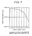
- FIG. 7 is a graph of a dependency on the doped Er amount of specific resistance in the Er doped BST thin film, respectively, which are graphed based on the measured results in Table 3. It can be seen from Table 3 and FIG. 5 that as compared to that tch of one whose doped Er amount (content) is zero, i.e.
- tch 500 hours or more and, specifically, those whose doped Er amount (content) is from 0.02 mol % to 0.2 mol % have a very excellent characteristic that tch is 1000 hours or more.
- containing no Er is 4.1 ⁇ 10 13 ⁇ cm
- those whose doped Er amount (content) is from 0.01 mol % to 0.25 mol % have an excellent characteristic that their specific resistance is 3.0 ⁇ 10 14 ⁇ cm or more and, specifically, those whose doped Er amount (content) is from 0.01 mol % to 0.2 mol % have a very excellent characteristic that their specific resistance is 5.0 ⁇ 10 14 ⁇ cm or more.
- characteristic time tch was prolonged in those STO thin films whose Er content is from 0.01 mol % to 0.2 mol % and a remarkable effect could be seen as against the degradation of the capacitor.
- the characteristic time tch was also prolonged in those BST thin films whose Er content is from 0.01 mol % to 0.25 mol % and a remarkable effect could be seen as against the degradation of the capacitor.
- the oxygen vacancies within the thin film may be reduced without degrading the dielectric constant and specifio resistance by containing Er to the dielectric thin film having the oxygen vacancies and composed of at least titanium and strontium, allowing to obtain the dielectric thin film capacitor element having an excellent reliability.
- the fabrication of the comparative example is different from that of the above-mentioned embodiment only in that a material obtained by fully mixing lanthanum oxide (La 2 O 3 ) with the SrTiO 3 powder so that lanthanum (La) concentration within the STO thin film turns out to be a desirable concentration, and sintering was used. That is, a material obtained by mixing the SrTiO 3 powder and the La 2 O 3 powder so that mole ratio thereof is 1 : x/200 in forming the STO thin film containing x mol % of La content, and sintering was used.
- a material obtained by fully mixing lanthanum oxide (La 2 O 3 ) with the SrTiO 3 powder so that lanthanum (La) concentration within the STO thin film turns out to be a desirable concentration, and sintering was used. That is, a material obtained by mixing the SrTiO 3 powder and the La 2 O 3 powder so that mole ratio thereof is 1 : x/200 in forming
- FIG. 8 shows the results obtained by studying the Er content within the STO thin film formed by implementing a plurality of times of formation by means of sputtering by using the same sputtering target so that the Er content within the STO thin film of the present embodiment turns out to be 0.05 mol % and the La content within the STO thin film formed by implementing a plurality of times of formation by means of sputtering by using the same sputtering target so that the La content within the STO thin film of the comparative example turns out to be 0.05 mol %. It can be seen from FIG.
- the dielectric thin film containing Er may be formed with a good reproducibility by using the sputtering which is excellent in productivity and the dielectric thin film capacitor element having a homogeneous characteristic may be manufactured with a high productivity.
Landscapes
- Engineering & Computer Science (AREA)
- Power Engineering (AREA)
- Microelectronics & Electronic Packaging (AREA)
- Manufacturing & Machinery (AREA)
- Ceramic Engineering (AREA)
- Chemical & Material Sciences (AREA)
- Inorganic Chemistry (AREA)
- Fixed Capacitors And Capacitor Manufacturing Machines (AREA)
- Semiconductor Memories (AREA)
- Ceramic Capacitors (AREA)
- Non-Volatile Memory (AREA)
- Inorganic Compounds Of Heavy Metals (AREA)
- Physical Vapour Deposition (AREA)
- Semiconductor Integrated Circuits (AREA)
Claims (8)
- Elément condensateur à film mince diélectrique comprenant :une électrode inférieure (4) ;un film mince diélectrique (5) ; etune électrode supérieure (6),l'électrode inférieure (4), le film mince diélectrique (5) et l'électrode supérieure (6) étant formés les uns après les autres sur un substrat (1),dans lequel le film mince diélectrique (5) est fait d'un matériau de type oxyde composé au moins de titane et de strontium et contient de l'erbium, caractérisé en ce que la teneur en erbium est de 0,01 à 0,2 % en moles.
- Elément condensateur à film mince diélectrique selon la revendication 1, dans lequel le film mince diélectrique (5) est fait de titanate de strontium contenant de 0,01 à 0,2 % en moles d'erbium.
- Elément condensateur à film mince diélectrique selon la revendication 2, dans lequel le film mince diélectrique (5) est fait de titanate de strontium contenant de 0,01 à 0,15 % en moles d'erbium.
- Elément condensateur à film mince diélectrique comprenant :une électrode inférieure (4) ;un film mince diélectrique (5) ; etune électrode supérieure (6),l'électrode inférieure (4), le film mince diélectrique (5) et l'électrode supérieure (6) étant formés l'un après l'autre sur un substrat (1),dans lequel le film mince diélectrique (5) est fait de titanate de baryum et de strontium contenant de l'erbium, caractérisé en ce que la teneur en erbium est de 0,01 à 0,25 % en moles.
- Elément condensateur à film mince diélectrique selon la revendication 4, dans lequel le film mince diélectrique (5) est fait de titanate de baryum et de strontium contenant de 0,01 à 0,2 % en moles d'erbium.
- Elément condensateur à film mince diélectrique selon la revendication 5, dans lequel le film mince diélectrique (5) est fait de titanate de baryum et de strontium contenant de 0,02 à 0,2 % en moles d'erbium.
- Procédé de fabrication d'un élément condensateur à film mince diélectrique comprenant une électrode inférieure (4), un film mince diélectrique (5) et une électrode supérieure (6) formés successivement sur un substrat (1), le procédé comprenant :
la formation d'un film mince de titanate de strontium contenant de l'erbium par un procédé de pulvérisation cathodique utilisant, en tant que cible de pulvérisation cathodique, un mélange de poudre de titanate de strontium et de poudre d'oxyde d'erbium contenant une proportion en moles d'oxyde d'erbium de 0,005 à 0,1 %. - Procédé de fabrication d'un élément condensateur à film mince diélectrique comprenant une électrode inférieure (4), un film mince diélectrique (5) et une électrode supérieure (6) formés successivement sur un substrat (1), le procédé comprenant :
la formation d'un film mince de titanate de baryum et de strontium contenant de l'erbium par un procédé de pulvérisation cathodique utilisant, en tant que cible de pulvérisation cathodique, un mélange de poudre de titanate de baryum et de strontium et de poudre d'oxyde d'erbium contenant une proportion en moles d'oxyde d'erbium de 0,005 à 0,15 %.
Applications Claiming Priority (3)
| Application Number | Priority Date | Filing Date | Title |
|---|---|---|---|
| JP145422/96 | 1996-06-07 | ||
| JP8145422A JPH09331020A (ja) | 1996-06-07 | 1996-06-07 | 誘電体薄膜キャパシタ素子及びその製造方法 |
| JP14542296 | 1996-06-07 |
Publications (3)
| Publication Number | Publication Date |
|---|---|
| EP0812021A2 EP0812021A2 (fr) | 1997-12-10 |
| EP0812021A3 EP0812021A3 (fr) | 1997-12-29 |
| EP0812021B1 true EP0812021B1 (fr) | 2001-10-17 |
Family
ID=15384891
Family Applications (1)
| Application Number | Title | Priority Date | Filing Date |
|---|---|---|---|
| EP97303886A Expired - Lifetime EP0812021B1 (fr) | 1996-06-07 | 1997-06-05 | Condensateur à film diélectrique mince et méthode de fabrication |
Country Status (4)
| Country | Link |
|---|---|
| US (1) | US5907470A (fr) |
| EP (1) | EP0812021B1 (fr) |
| JP (1) | JPH09331020A (fr) |
| DE (1) | DE69707356T2 (fr) |
Families Citing this family (22)
| Publication number | Priority date | Publication date | Assignee | Title |
|---|---|---|---|---|
| JP3337622B2 (ja) * | 1997-07-16 | 2002-10-21 | 松下電器産業株式会社 | 選択的エッチング液及びそのエッチング液を用いた半導体装置の製造方法 |
| US6245203B1 (en) * | 1997-10-01 | 2001-06-12 | Japan Energy Corporation | BaxSr1-xTiO3-y target materials for sputtering |
| JP3171170B2 (ja) * | 1998-05-25 | 2001-05-28 | 日本電気株式会社 | 薄膜キャパシタおよびその製造方法 |
| JP2000236075A (ja) * | 1999-02-12 | 2000-08-29 | Sony Corp | 誘電体キャパシタの製造方法および半導体記憶装置の製造方法 |
| EP1153434A1 (fr) * | 1999-02-17 | 2001-11-14 | International Business Machines Corporation | Dispositif micro-electronique de stockage de l'information et son procede d'utilisation |
| US6281142B1 (en) * | 1999-06-04 | 2001-08-28 | Micron Technology, Inc. | Dielectric cure for reducing oxygen vacancies |
| US6103567A (en) * | 1999-08-10 | 2000-08-15 | Vanguard International Semiconductor Corp. | Method of fabricating dielectric layer |
| US6774077B2 (en) * | 2001-01-24 | 2004-08-10 | Paratek Microwave, Inc. | Electronically tunable, low-loss ceramic materials including a tunable dielectric phase and multiple metal oxide phases |
| US6801104B2 (en) * | 2000-08-22 | 2004-10-05 | Paratek Microwave, Inc. | Electronically tunable combline filters tuned by tunable dielectric capacitors |
| AU2001296281A1 (en) | 2000-09-21 | 2002-04-02 | Michaeld. Casper | Integrated thin film capacitor/inductor/interconnect system and method |
| US7327582B2 (en) * | 2000-09-21 | 2008-02-05 | Ultrasource, Inc. | Integrated thin film capacitor/inductor/interconnect system and method |
| US6890629B2 (en) | 2001-09-21 | 2005-05-10 | Michael D. Casper | Integrated thin film capacitor/inductor/interconnect system and method |
| US8609017B2 (en) * | 2001-01-24 | 2013-12-17 | Blackberry Limited | Electronically tunable, low-loss ceramic materials including a tunable dielectric phase and multiple metal oxide phases |
| US7425877B2 (en) * | 2001-09-21 | 2008-09-16 | Ultrasource, Inc. | Lange coupler system and method |
| US6998696B2 (en) | 2001-09-21 | 2006-02-14 | Casper Michael D | Integrated thin film capacitor/inductor/interconnect system and method |
| US6909592B2 (en) * | 2003-01-30 | 2005-06-21 | Dongbuanam Semiconductor Inc. | Thin film capacitor and fabrication method thereof |
| WO2005008757A1 (fr) * | 2003-07-16 | 2005-01-27 | Showa Denko K.K. | Electrode ohmique de type n destinee a un semiconducteur de nitrure du groupe iii de type n, dispositif a semiconducteurs electroluminescent comportant cette electrode, et procede de fabrication d'une electrode ohmique de type n |
| JP4523299B2 (ja) * | 2003-10-31 | 2010-08-11 | 学校法人早稲田大学 | 薄膜コンデンサの製造方法 |
| EP1587137A1 (fr) * | 2004-04-16 | 2005-10-19 | International Business Machines Corporation | Procédé de dépôt d'une mémoire non-volatile à commutation de résistance |
| US7582549B2 (en) | 2006-08-25 | 2009-09-01 | Micron Technology, Inc. | Atomic layer deposited barium strontium titanium oxide films |
| US9013002B1 (en) * | 2011-12-02 | 2015-04-21 | The United States Of America As Represented By The Administrator Of National Aeronautics And Space Administration | Iridium interfacial stack (IRIS) |
| CN109637809B (zh) * | 2018-12-21 | 2022-03-11 | 广州天极电子科技股份有限公司 | 一种陶瓷储能电容器及其制备方法 |
Family Cites Families (10)
| Publication number | Priority date | Publication date | Assignee | Title |
|---|---|---|---|---|
| WO1991015023A1 (fr) * | 1990-03-28 | 1991-10-03 | Taiyo Yuden Kabusikigaisha | Condensateur en ceramique et production de ce condensateur |
| JPH0734327B2 (ja) * | 1990-09-05 | 1995-04-12 | 株式会社村田製作所 | 非還元性誘電体磁器組成物 |
| DE69327815T2 (de) * | 1992-05-29 | 2000-08-17 | Texas Instruments Inc., Dallas | Donatoren-dotierte Perovskite für Dünnfilm-Dielektrika |
| DE69404189T2 (de) * | 1993-03-31 | 1998-01-08 | Texas Instruments Inc | Leicht donatoren-dotierte Elektroden für Materialien mit hoher dielektrischer Konstante |
| US5471364A (en) * | 1993-03-31 | 1995-11-28 | Texas Instruments Incorporated | Electrode interface for high-dielectric-constant materials |
| JPH0773732A (ja) * | 1993-06-23 | 1995-03-17 | Sharp Corp | 誘電体薄膜素子及びその製造方法 |
| US5548475A (en) * | 1993-11-15 | 1996-08-20 | Sharp Kabushiki Kaisha | Dielectric thin film device |
| US5453908A (en) * | 1994-09-30 | 1995-09-26 | Texas Instruments Incorporated | Barium strontium titanate (BST) thin films by holmium donor doping |
| US5635741A (en) * | 1994-09-30 | 1997-06-03 | Texas Instruments Incorporated | Barium strontium titanate (BST) thin films by erbium donor doping |
| JP3024537B2 (ja) * | 1995-12-20 | 2000-03-21 | 株式会社村田製作所 | 積層セラミックコンデンサ |
-
1996
- 1996-06-07 JP JP8145422A patent/JPH09331020A/ja active Pending
-
1997
- 1997-06-05 DE DE69707356T patent/DE69707356T2/de not_active Expired - Lifetime
- 1997-06-05 EP EP97303886A patent/EP0812021B1/fr not_active Expired - Lifetime
- 1997-06-06 US US08/870,629 patent/US5907470A/en not_active Expired - Lifetime
Also Published As
| Publication number | Publication date |
|---|---|
| EP0812021A3 (fr) | 1997-12-29 |
| DE69707356T2 (de) | 2002-07-04 |
| JPH09331020A (ja) | 1997-12-22 |
| DE69707356D1 (de) | 2001-11-22 |
| EP0812021A2 (fr) | 1997-12-10 |
| US5907470A (en) | 1999-05-25 |
Similar Documents
| Publication | Publication Date | Title |
|---|---|---|
| EP0812021B1 (fr) | Condensateur à film diélectrique mince et méthode de fabrication | |
| Hwang et al. | Deposition of extremely thin (Ba, Sr) TiO3 thin films for ultra‐large‐scale integrated dynamic random access memory application | |
| KR100274512B1 (ko) | 집적회로커패시터 및 그 제조방법 | |
| EP0709355B1 (fr) | Couche diélectrique mince de titanate de barium et/ou strontium comprenant de l'erbium, et procédé de formation | |
| EP0562101B1 (fr) | Condensateur a tension variable ayant un film dielectrique amorphe | |
| KR100325048B1 (ko) | 박막 캐패시터 및 그 제조 방법 | |
| KR100355585B1 (ko) | 박막커패시터 | |
| KR20010031913A (ko) | 유전체 소자와 그 제조 방법 | |
| KR100478748B1 (ko) | 비스무스층구조의강유전성박막형성방법 | |
| KR102259923B1 (ko) | 유전박막, 이를 포함하는 멤커패시터, 이를 포함하는 셀 어레이, 및 그 제조 방법 | |
| US20020031919A1 (en) | Method for improving the sidewall stoichiometry of thin film capacitors | |
| US20060131627A1 (en) | Ferroelectric material, its manufacture method and ferroelectric memory | |
| US6548342B1 (en) | Method of producing oxide dielectric element, and memory and semiconductor device using the element | |
| US6258655B1 (en) | Method for improving the resistance degradation of thin film capacitors | |
| US6437380B1 (en) | Ferroelectric device with bismuth tantalate capping layer and method of making same | |
| KR20070089638A (ko) | 반도체 장치 및 반도체 장치의 제조 방법 | |
| Duen~ as et al. | Use of anodic tantalum pentoxide for high-density capacitor fabrication | |
| US6504228B1 (en) | Semiconductor device and method for manufacturing the same | |
| JPH09129827A (ja) | 強誘電体キャパシタ | |
| JPH10214947A (ja) | 薄膜誘電体素子 | |
| KR100335494B1 (ko) | Bst 유전막에 구리를 함유한 커패시터 및 그 제조방법 | |
| JP2001358303A (ja) | 薄膜キャパシタおよびその製造方法 | |
| KR20000029860A (ko) | 반도체장치및그제조방법 | |
| GB2314348A (en) | Thin film formation of a dielectric | |
| US20040165334A1 (en) | Multi-layered unit |
Legal Events
| Date | Code | Title | Description |
|---|---|---|---|
| PUAI | Public reference made under article 153(3) epc to a published international application that has entered the european phase |
Free format text: ORIGINAL CODE: 0009012 |
|
| PUAL | Search report despatched |
Free format text: ORIGINAL CODE: 0009013 |
|
| AK | Designated contracting states |
Kind code of ref document: A2 Designated state(s): DE FR GB |
|
| AK | Designated contracting states |
Kind code of ref document: A3 Designated state(s): AT BE CH DE DK ES FI FR GB GR IE IT LI LU MC NL PT SE |
|
| 17P | Request for examination filed |
Effective date: 19980108 |
|
| AKX | Designation fees paid |
Free format text: DE FR GB |
|
| RBV | Designated contracting states (corrected) |
Designated state(s): DE FR GB |
|
| 17Q | First examination report despatched |
Effective date: 19991201 |
|
| GRAG | Despatch of communication of intention to grant |
Free format text: ORIGINAL CODE: EPIDOS AGRA |
|
| GRAG | Despatch of communication of intention to grant |
Free format text: ORIGINAL CODE: EPIDOS AGRA |
|
| GRAH | Despatch of communication of intention to grant a patent |
Free format text: ORIGINAL CODE: EPIDOS IGRA |
|
| GRAH | Despatch of communication of intention to grant a patent |
Free format text: ORIGINAL CODE: EPIDOS IGRA |
|
| GRAA | (expected) grant |
Free format text: ORIGINAL CODE: 0009210 |
|
| AK | Designated contracting states |
Kind code of ref document: B1 Designated state(s): DE FR GB |
|
| REF | Corresponds to: |
Ref document number: 69707356 Country of ref document: DE Date of ref document: 20011122 |
|
| REG | Reference to a national code |
Ref country code: GB Ref legal event code: IF02 |
|
| ET | Fr: translation filed | ||
| PLBE | No opposition filed within time limit |
Free format text: ORIGINAL CODE: 0009261 |
|
| STAA | Information on the status of an ep patent application or granted ep patent |
Free format text: STATUS: NO OPPOSITION FILED WITHIN TIME LIMIT |
|
| 26N | No opposition filed | ||
| PGFP | Annual fee paid to national office [announced via postgrant information from national office to epo] |
Ref country code: GB Payment date: 20140604 Year of fee payment: 18 |
|
| PGFP | Annual fee paid to national office [announced via postgrant information from national office to epo] |
Ref country code: DE Payment date: 20140528 Year of fee payment: 18 |
|
| PGFP | Annual fee paid to national office [announced via postgrant information from national office to epo] |
Ref country code: FR Payment date: 20140609 Year of fee payment: 18 |
|
| REG | Reference to a national code |
Ref country code: DE Ref legal event code: R119 Ref document number: 69707356 Country of ref document: DE |
|
| GBPC | Gb: european patent ceased through non-payment of renewal fee |
Effective date: 20150605 |
|
| REG | Reference to a national code |
Ref country code: FR Ref legal event code: ST Effective date: 20160229 |
|
| PG25 | Lapsed in a contracting state [announced via postgrant information from national office to epo] |
Ref country code: GB Free format text: LAPSE BECAUSE OF NON-PAYMENT OF DUE FEES Effective date: 20150605 Ref country code: DE Free format text: LAPSE BECAUSE OF NON-PAYMENT OF DUE FEES Effective date: 20160101 |
|
| PG25 | Lapsed in a contracting state [announced via postgrant information from national office to epo] |
Ref country code: FR Free format text: LAPSE BECAUSE OF NON-PAYMENT OF DUE FEES Effective date: 20150630 |