EP0812497B1 - Systeme emetteur-recepteur hertzien pour communication numerique - Google Patents
Systeme emetteur-recepteur hertzien pour communication numerique Download PDFInfo
- Publication number
- EP0812497B1 EP0812497B1 EP96907159A EP96907159A EP0812497B1 EP 0812497 B1 EP0812497 B1 EP 0812497B1 EP 96907159 A EP96907159 A EP 96907159A EP 96907159 A EP96907159 A EP 96907159A EP 0812497 B1 EP0812497 B1 EP 0812497B1
- Authority
- EP
- European Patent Office
- Prior art keywords
- signal
- power
- processing
- conductive cable
- transceiver system
- Prior art date
- Legal status (The legal status is an assumption and is not a legal conclusion. Google has not performed a legal analysis and makes no representation as to the accuracy of the status listed.)
- Expired - Lifetime
Links
- 238000004891 communication Methods 0.000 title description 14
- 238000012545 processing Methods 0.000 claims description 31
- 230000005540 biological transmission Effects 0.000 claims description 25
- 238000001514 detection method Methods 0.000 claims description 15
- 238000000034 method Methods 0.000 claims description 12
- 230000010355 oscillation Effects 0.000 claims description 8
- 230000004044 response Effects 0.000 claims description 7
- 230000001902 propagating effect Effects 0.000 claims description 2
- 230000000644 propagated effect Effects 0.000 claims 1
- 230000008901 benefit Effects 0.000 description 9
- 230000001413 cellular effect Effects 0.000 description 9
- 238000010586 diagram Methods 0.000 description 8
- 230000006870 function Effects 0.000 description 6
- 239000003990 capacitor Substances 0.000 description 5
- 230000007423 decrease Effects 0.000 description 5
- 230000007613 environmental effect Effects 0.000 description 5
- 238000001228 spectrum Methods 0.000 description 5
- 230000001276 controlling effect Effects 0.000 description 3
- 238000010248 power generation Methods 0.000 description 2
- 230000003321 amplification Effects 0.000 description 1
- 230000008859 change Effects 0.000 description 1
- 238000012937 correction Methods 0.000 description 1
- 238000011161 development Methods 0.000 description 1
- 230000009977 dual effect Effects 0.000 description 1
- 238000005516 engineering process Methods 0.000 description 1
- 239000000835 fiber Substances 0.000 description 1
- 238000003199 nucleic acid amplification method Methods 0.000 description 1
- 230000008569 process Effects 0.000 description 1
- 230000001105 regulatory effect Effects 0.000 description 1
- 230000035945 sensitivity Effects 0.000 description 1
- 230000008054 signal transmission Effects 0.000 description 1
- 230000007480 spreading Effects 0.000 description 1
Images


Classifications
-
- H—ELECTRICITY
- H04—ELECTRIC COMMUNICATION TECHNIQUE
- H04W—WIRELESS COMMUNICATION NETWORKS
- H04W52/00—Power management, e.g. Transmission Power Control [TPC] or power classes
- H04W52/04—Transmission power control [TPC]
- H04W52/52—Transmission power control [TPC] using AGC [Automatic Gain Control] circuits or amplifiers
-
- H—ELECTRICITY
- H04—ELECTRIC COMMUNICATION TECHNIQUE
- H04B—TRANSMISSION
- H04B1/00—Details of transmission systems, not covered by a single one of groups H04B3/00 - H04B13/00; Details of transmission systems not characterised by the medium used for transmission
- H04B1/38—Transceivers, i.e. devices in which transmitter and receiver form a structural unit and in which at least one part is used for functions of transmitting and receiving
- H04B1/3827—Portable transceivers
- H04B1/3877—Arrangements for enabling portable transceivers to be used in a fixed position, e.g. cradles or boosters
-
- H—ELECTRICITY
- H04—ELECTRIC COMMUNICATION TECHNIQUE
- H04B—TRANSMISSION
- H04B7/00—Radio transmission systems, i.e. using radiation field
- H04B7/005—Control of transmission; Equalising
Definitions
- the present invention relates to wireless telecommunications. More particularly, the present invention relates to a radio frequency transceiver system for interfacing radio frequency signals with digital modems used for wireless telecommunication.
- Wireless telephone systems provide telephone service via the use of a subscriber unit and base station that communicate with each other using radio frequency (RF) signals.
- the subscriber unit provides an individual, called a "subscriber", with an interface to the base station and the base station provides the subscriber unit with an interface to a call processing center.
- Cellular wireless telephone systems incorporate the use of multiple base stations scattered over a given area thereby allowing the subscriber unit to be used in a highly mobile fashion.
- the subscriber unit often resembles a compact telephone hand-set having an antenna, and is normally carried by the subscriber during operation to make and receive telephone calls in a completely mobile fashion.
- Digital wireless telephone systems process and transmit the data associated with a communication session or phone call in various specialized manners in order to utilize the available RF bandwidth more efficiently than analog wireless telephone systems.
- the subscriber unit for a digital wireless telephone system includes a modem that converts both voice and data information between analog and digital signal formats, and an RF transceiver system including an antenna and RF signal processing circuitry.
- the modem is configured to properly demodulate signals provided by the transceiver system that are within a range of decibel (dB) levels that correspond to the range of distances from the base station in which the subscriber unit is expected to operate.
- dB decibel
- CDMA Code division multiple access
- CDMA digital wireless telecommunication systems place the RF signals used for communication in a spread spectrum waveform via the use of a spreading code in order to further increase RF bandwidth efficiency of the system.
- the strength of the outgoing signal is varied substantially over time in a tightly controlled manner to reduce the interference between RF signals generated by the various subscriber units. This allows the maximum number of communication sessions to be carried out over a given amount of RF bandwidth. Because of this substantial amount of power variation, however, power limiting is also performed to ensure that the transceiver system is not damaged from overloading.
- the transceiver system and modem that make up a subscriber unit for a digital wireless telephone system are generally kept in close proximity to each other during operation. This is done primarily to keep the subscriber unit compact for purposes of mobility, which has traditionally been the main advantage of wireless telephone systems. Other advantages are also provided by the compact configuration, however.
- One advantage is that the sensitivity to environmental variations of the subscriber unit is reduced by keeping the length of the connections between the systems that make up the subscriber unit small. This reduces the concern that these environmental parameters will affect the performance of the subscriber unit.
- the signal processing circuitry within the transceiver system is located in dose proximity to the antenna. This allows the incoming, or receive (Rx), signal to be processed after reception by the antenna with as little signal loss and noise introduction as possible.
- keeping the subscriber unit compact facilitates the exchange of control signals between the modem and the transceiver system. This allows the two systems to cooperate when performing various functions including the power limiting function described above within the context of a CDMA wireless telephone system.
- Compact configuration of the subscriber unit does not necessarily provide for optimal transmission and reception of the RF signals used to conduct wireless communication, however. This is because the subscriber unit is normally located near the subscriber during use, and the subscriber is often in a poor location for the reception and transmission of RF signals including within a building or behind a hill. This less than optimal placement of the transceiver systems is tolerated, however, because of the various benefits created by compact configuration of the subscriber unit described above, including mobility.
- the concentrated subscriber system provides wireless telephone service at a reduced cost when compared to previous wireless telephone systems by allowing multiple subscribers to interface with a base station via RF signals using a set of shared modems and a transceiver system.
- the modems used within the subscriber system are the same or similar to those used in prior art mobile subscriber units so that the development cost of the concentrated subscriber system is reduced.
- the concentrated subscriber system is placed in a fixed location during use that can be within as great or greater range of distances from the base station than those experienced by the prior art mobile subscriber unit. This is because the concentrated subscriber unit is intended to provide inexpensive non-mobile telephone service both in areas where mobile telephone service is and is not available, and therefore in areas where a base station may or may not be close by.
- the concentrated subscriber system incorporates the use of CDMA wireless telephone system technology.
- the concentrated subscriber system is not mobile during use there is no need for compactness as with the prior art mobile subscriber unit. Therefore, the reception of the concentrated subscriber system can be improved by positioning the antenna away from the subscriber in a location having improved RF signal transmission and reception capability.
- the concentrated subscriber system since the concentrated subscriber system untilizes the digital modems from the standard mobile subscriber unit in the preferred embodiment to reduce cost, but can be located at a greater range of distances from the base station during use, it is also desirable to have that transceiver system adjust the strength of the Rx signal to the range of decibel levels in which the modems were originally designed to operate, so that processing of the signals by the modems may proceed properly.
- EP-A-0,622,907 describes a procedure for using a radio phone with an external amplifying means for receiving, amplifying and transmitting a radio frequency reception signal to the radio phone, in which radio phone a reception frequency signal is supplied to a front end amplifier.
- the control signal is preferably a voltage control signal of direct voltage frequency or low frequency produced in the amplifying means, which in the amplifying means is added into the reception signal, and in the radio phone separated from the reception signal into a control signal of the front end amplifier.
- GB-A-2,253,119 describes a telecommunications adaptor that enables a fixed telephone system, adapted for use with the public switched telephone network (PSTN), to operate over a radio telecommunications network the fixed telephone system is adapted to operate over a personal communications network (PCN).
- PSTN public switched telephone network
- PCN personal communications network
- the connection of the wiring loop of the fixed telephone system to the PSTN is severed at the entry point to the residence and a telecommunications adaptor connected into the wiring loop.
- the adaptor has an antenna for transmitting and receiving radio signals to and from the PCN.
- the transceiver system for the wireless telephone concentrated subscriber system that allows an antenna to be placed in a location having optimal reception and that can interface with existing or minimally modified digital modems.
- the transceiver system includes an antenna, an antenna interface system and modem interface system separated by a coaxial cable.
- the antenna is placed in a location having optimal reception such as the roof of a building and in close proximity to the antenna interface system.
- the coaxial cable couples the antenna interface system to the modem interface system which is placed within the building so that it may be easily accessed for service and configuration, and so that it may be coupled to the rest of the concentrated subscriber system.
- the modem interface system includes a two state variable attenuator and an attenuation register that are configured to either reduce the strength of the incoming signal when the concentrated subscriber system is located near a base station, or to pass the incoming signal without attenuation when the concentrated subscriber unit is at a more distant location.
- a signal loss detection system fixes the amount of signal loss experienced by the "receive" (Rx) signal before being supplied to the modems and the transmit (Tx) signal before being provided to the antenna as the environmental conditions change.
- the signal loss detection systems includes a detector located in the modem interface system that receives an oscillating signal transmitted from the antenna interface system through the coaxial cable and an attenuator controlled by the detector.
- a differential integrator within the signal loss detection system determines the difference between oscillating signal and a reference value accordingly so the loss experienced by the Rx and Tx signals remains constant or is "normalized".
- the antenna interface system allows multiple modems to generate a signal using a single power amplifier circuit by including a maximum power limiting system that detects when the signal being generated exceeds the capacity of the transmit power amplifier, and that transmits an alarm signal to the modem interface system in response so that the modem interface system can signal the rest of the concentrated subscriber system.
- a wireless telephone transceiver system comprising means for receiving and transmitting radio wave signals; first means for processing the radio wave signals coupled to the means for receiving and transmitting that places the radio wave signals in condition for transmission, the first means including means for amplifying the radio wave signals with minimum noise introduction following reception thereof by the means for receiving and transmitting radio wave signals, and power amplifier means, coupled to means for receiving and transmitting radio wave signals, for generating an outgoing radio frequency signal for transmission by the means for receiving and transmitting radio wave signals; a conductive cable for propagating the radio wave signals, the conductive cable having a first end and a second end wherein the first end is coupled to the first means for processing; and a second means for processing radio wave signals, coupled to the second end of the conductive cable, that places the radio waves in condition for demodulation.
- the system is characterised by: the first means further including: variable attenuator means coupled to the power amplifier means for attenuating the outgoing radio wave signal prior to transmission, and a power output detection means for controlling the variable attenuator means by generating and applying an attenuation signal to the variable attenuator means when the power amplifier means generates a signal having a power level greater than a predetermined level; a third means coupled to the conductive cable for introducing a first oscillating signal into the conductive cable and determining a signal loss amount experienced by said first oscillating signal when transmitted over the conductive cable; and a fourth means for generating a second oscillation signal in response to the attenuation signal, the fourth means being coupled to the power output detection means and the conductive cable, wherein the second oscillation signal is transmitted through the conductive cable for use in further controlling the power of the signal generated by the power amplifer means.
- a concentrated subscriber transceiver system comprising the wireless telephone transceiver system according to the first aspect of the invention and a bank of modems; wherein the modem interface system is coupled to the bank of modems; and the modem interface system is arranged for processing radio frequency signals received from the bank of modems for transmission to the antenna interface system and for processing radio frequency signals received from the antenna interface system for transmission to the bank for modems.
- a method of processing radio frequency signals comprising receiving a radio frequency signal by receiving the radio frequency signal using an antenna, amplifying the radio frequency signal using a low noise amplifier, passing the radio frequency signal and a first oscillating signal over a conductive cable, determining an amount of signal loss introduced by the conductive cable using the first oscillating signal, and attenuating the radio frequency signal based upon the amount of signal loss, and transmitting a radio frequency signal by generating an output signal for transmission by the antenna using a power amplifier, and generating a second oscillating signal for transmission over the conductive cable when the power amplifier generates a signal having a power level greater than a predetermined level, for use in further controlling the power level of the signal.
- a method and apparatus for providing radio frequency interface to a concentrated subscriber system is described.
- the following description is within the context of a code division multiple access digital cellular telephone system. It will be apparent to one skilled in the art that embodiments of the invention may be practiced within a variety of radio based wireless telecommunication systems using digital or analog modulation using single or multiple base stations, or satellite based gateways. Also while a coaxial cable is used in the following description, the use of other wire based transmission media will be apparent. In various other instances variable attenuation of certain signals is performed in order to achieve desired decibel level. It will be understood that variable amplification of these signals may be used to provide similar results. Also in the following description, various well known systems and interfaces are provided in block form. This is done in order to avoid unnecessarily obscuring the disclosure of the present invention.
- Fig. 1 is a block diagram of a cellular telephone system configured in accordance with one embodiment of the present invention.
- Base transceiver station 102 transmits and receives radio frequency (RF) signals to and from remote communication units 100 and 112 .
- RF radio frequency
- these RF signals are modulated in accordance with the CDMA spread spectrum techniques described in US Patent Number 4,901,307 ('307) entitled “Spread Spectrum Multiple Access Communication System Using a Satellite or Terrestrial Repeater", and US Patent Number 5,103,459 ('459) entitled “System and Method for Generating Signal Wave Forms in a CDMA Cellular Telephone System” assigned to QUALCOMM TM Incorporated as well as in specification IS-95 from the Telecommunication Industry Association (2001 Pennsylvania Avenue, Suite 800, Washington, DC 20006) entitled “Mobile Station-Base Station Compatibility Standard for Dual Mode Wideband Spread Spectrum Cellular System” (IS-95).
- RF radio frequency
- base transceiver station 102 interfaces with base station controller (BSC) 104 in any one of a variety of manners including microwave link, ground base wire connections, fiber optic cable, or a combination thereof, BSC 104 interfaces with public telephone switching network (PSTN) 106 through mobile switching center (MSC) 105 allowing various communication sessions or telephone calls to be delivered between base transceiver station 102 , base transceiver station 110 , and other base transceiver stations 108 .
- PSTN public telephone switching network
- MSC mobile switching center
- Base transceiver station 110 interfaces with BSC 104 in a similar manner as base transceiver station 102 and communicates with remote communication unit 112 and concentrated subscriber system (CSS) 113 via RF signals modulated in accordance with the above reference patent '459 and '307 and specification IS-95.
- CSS concentrated subscriber system
- subscriber units 116(1) through (50) are coupled to CSS controller 114 which performs the interface function with base transceiver station 110 .
- Subscriber units 116(1) through (50) each are used in a manner similar to a standard telephone to initiate and receive telephone calls and may be standard wire based, pulse code modulated telephone sets in some instances, or other types of telephone sets having a microphone and speaker.
- CSS controller 114 is shown coupled directly to subscriber units 116 , alternative methods for exchanging information are contemplated including a simplified form of radio wave based communication. Additionally, alternative numbers of subscriber units 116 may be coupled to CSS controller 114 other than the fifty units indicated.
- Fig. 2 is a block diagram of CSS controller 114 of Fig. 1 configured in accordance with the described embodiment of the invention.
- Antenna interface system 270 transmits and receives spread spectrum modulated RF signals to and from base transceiver station 110 of Fig. 1 through antenna 250 .
- the received signals are supplied through coaxial cable 251 and modem interface system 252 to modem bank 260 which is comprised of modems 262(1) through (16) .
- the transmitted signals are generated by modem bank 260 and transmitted through modem interface system 252 and coaxial cable 251 to antenna interface system 270 which supplies the signals to antenna 250 .
- Multiplexer system 266 couples subscriber lines 256(1) through (50) to modems 262(1) through (16) of modem bank 260 .
- Control system 254 receives and provides information to modem bank 260 and controls multiplexer system 266 using information stored in memory sub-system 253 .
- the operation and configuration of control system 254 as well as modems 262 and multiplexer system 266 is described in the above referenced co-pending application "Concentrated Subscriber System for Wireless Local Loop.” While sixteen modems are shown the use of different numbers of modems is consistent with the operation of the invention.
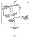
- Fig. 3 is a block diagram of antenna interface system 270 when configured in accordance with one embodiment of the invention.
- Duplexer 302 is coupled to the input of low noise amplifier 304 and the output of coupler 305 as well as to antenna 250 .
- Duplexer 312 is coupled to the output of low noise amplifier 304 and the input of variable attenuator 313 as well as to coaxial cable 251 .
- Transmit power amplifier 306 is placed between coupler 305 and variable antenuator 313 .
- Detector 307 is coupled via coupler 305 to the output of transmit power amplifier 306 and to the input of differential integrator 309 which has a reference voltage applied to the other input.
- differential integrator 309 The output of differential integrator 309 is applied to the control input of variable antenuator 313 and to low frequency oscillator 316.
- Inductor 322 connects low frequency oscillator 316 and power distribution system 300 to coaxial cable 251 .
- High frequency oscillator 325 is coupled to coaxial cable 251 through capacitor 321 , resistor 329 and lowpass filter 330 .
- Power amplifier 306 and low noise amplifier 304 may be formed by a series of amplifier and filter circuits placed in various locations within the signal path but are shown as a single system for ease of drawing.
- a receive (Rx) signal received by antenna 250 is passed to duplexer 302 which directs the carrier signal to low noise amplifier 304 .
- Low noise amplifier 304 amplifies the relatively weak Rx carrier signal to a decibel level range greater than the decibel level range properly demodulated by one of modems 262 by an amount that is at least as much as the maximum expected signal loss introduced by co-axial cable 251 and any other intermediate circuitry.
- the amplified Rx carrier signal is then transmitted through duplexer 312 and coaxial cable 251 to modem interface system 252 (Fig. 2) .
- Outgoing or transmit (Tx) signals transmitted from modem interface system 252 through coaxial cable 251 are directed by duplexer 312 to variable attenuator 313 which passes the signal to power amplifier 306 .
- the resulting amplified signal generated at the output of power amplifier 306 is passed through coupler 305 and duplexer 302 to antenna 250 from which it is transmitted to base transceiver station 110 of Fig. 1.
- Detector 307 receives a signal from coupler 305 that is substantially proportional to the Tx carrier signal at the output of power amplifier 306 and asserts a proportional DC voltage that is applied to differential integrator 309 . While the use of a proportional relationship between the signals at the input and output of detector 307 is preferred, other relationships that are indicative of the power being generated by power amplifier 306 may also be used and will be apparent to one skilled in the art.
- Differential integrator 309 generates another DC voltage signal based on the difference between the DC voltage from detector 307 and the reference voltage. If the voltage from detector 307 is less than the reference voltage, the second DC voltage from differential integrator 309 is placed at a first level which in the preferred embodiment is eleven volts, although any other voltage level may be easily substituted.
- differential integrator 309 begins to decrease in proportion to the difference between the DC voltage from detector 307 and the reference voltage.
- Variable attenuator 313 responds to this decrease in the voltage asserted by differential integrator 309 by introducing attenuation into the transmit signal received from duplexer 312 . This attenuation is increased in proportion to the amount the voltage asserted by differential integrator 309 decreases. Additionally, when the DC voltage from differential integrator 309 begins to decrease below eleven volts, low frequency oscillator 316 begins to generate a low frequency signal that is transmitted through inductor 322 and coaxial cable 251 to modem interface system 252 . This low frequency signal forms a power alarm signal that is used by modem interface system 252 and control system 254 to perform further power control functions.
- High frequency oscillator 325 constantly generates a signal loss detection signal that has a frequency dose to the frequencies of the Rx and Tx signal over which the various telephone calls and other communication sessions are carried.
- this frequency should be sufficiently dose to the Rx and Tx signals that the frequency loss detection signal experiences a signal loss that is similar to that experienced by the Rx and Tx signals when transmitted over coaxial cable 251 .
- the use of signal loss detection signals having a frequency that are not close to the frequency of the Tx or Rx signals is also consistent with the operation of the invention. Additionally, the strength of this signal loss detection signal is tightly controlled so that the amount of loss it experiences from transmission through the coaxial cable can be measured.
- the signal loss detection signal is transmitted through lowpass filter 330 , capacitor 321 and resistor 329 to coaxial cable 251 which passes the signal to modem interface system 252 .
- Power distribution system 300 receives a DC voltage from modem interface system 252 over coaxial cable 251 and distributes the power to the various other systems that make up antenna interface system 270 through connections that are not shown for ease of drawing.
- Fig. 4 is a block diagram of modem interface system 252 when configured in accordance with one embodiment of the invention.
- the amplified Rx signal from antenna interface system 270 of Fig. 3 is passed by coaxial cable 251 to variable antenuator 350 through capacitor 352 .
- the signal from attenuator 350 then passes through coupler 355 , attenuator 354 , duplexer 356, to low noise amplifier 358.
- Low noise amplifier 358 amplifies the signal and supplies it to splitter 360 which splits it into four signals that are provided to four modem systems (not shown), each of which has four modems that make up the sixteen modems of modem bank 260 .
- Tx signal is then passed through capacitor 352 and coaxial cable 251 to antenna interface system 270 .
- Power generation system 380 is coupled to coaxial cable 251 through inductor 382 .
- Bandpass filter 366 receives a signal from coupler 355 that is proportional to the signal at the output of attenuator 350 and filters out most of the noise and signal not at the frequency of the signal generated by high frequency oscillator 325 of Fig. 3 . This causes the signal from high frequency oscillator 325 to pass to detector 368 which generates a corresponding DC voltage that is applied to the input of differential integrator 370 . Differential integrator 370 generates a DC voltage based on the difference between the voltage from detector 368 and the reference voltage applied to its other input that is applied to variable attenuator 350 .
- the signal from differential integrator 370 causes variable attenuator 350 to reduce the strength of the carrier signal from antenna interface system 270 accordingly such that the loss introduced by coaxial cable 251 will be normalized and the signal can be placed within a decibel range that can easily and properly demodulated by one of the modems 262 of modem bank 260.
- the reference voltage is applied to differential integrator 370 such that the attenuation introduced by variable attenuator 350 is reduced as the signal loss introduced by coaxial cable 251 increases thereby fixing the amount of signal loss introduced into the signal as it travels between the antenna interface card and the modem interface card.
- the amount of signal loss is set to the maximum amount of loss expected from coaxial cable 251 alone placed in the least optimal configuration and conditions. This allows the signal strength applied to the modems to remain constant despite varying lengths of coaxial cable 251 and varying operating environments and temperatures.
- Power generation system 380 provides DC through coaxial cable 251 and inductor 382 to antenna interface system 270 .
- Bandpass filter 372 allows the low frequency signal generated by low frequency oscillator 316 of Fig. 3 to pass to detector 374 after being transmitted through inductor 377 and capacitor 378 .
- detector 374 receives this low frequency signal, it generates a power alarm signal that is applied to control system 254 of Fig. 2 .
- UHF adjust register 376 is set to either activate or deactivate attenuator 354 depending on the distance concentrated subscriber system 113 of Fig. 1 is from base transceiver station 110 of Fig. 1. If the concentrated subscriber system is located in dose proximity to the base transceiver station the register is set to activate attenuator 354 so that the strength of the signal received by duplexer 356 is reduced.
- UHF adjust register 376 is set to deactivate attenuator 354 so that the signal strength applied to duplexer 356 is not reduced. This provides the concentrated subscriber system with increased dynamic range for receiving and transmitting signals, and therefore increases the range of distances in which it can properly interact with base transceiver station 110.
- the transmit carrier signal from modem bank 260 of Fig. 2 and summer 362 of Fig. 4 is also transmitted through attenuators 354 and 350 which helps ensure that the difference between the decibel level of the receive and transmit carrier signals remains within a predetermined range which in the preferred embodiment is that proscribed by the IS-95 specification. However, it is also contemplated that the Tx carrier signal could bypass antenuator 354 if such a configuration was desirable.
- a concentrated subscriber system can be implemented that has improved transmission and reception capability. This is because when such a transceiver system is incorporated into a concentrated subscriber system, the antenna can be placed in a remote location where the RF signals used for communication can be transmitted and received more easily while the subscriber units remain in dose proximity to the subscribers.
- the ability to use the coaxial cable to connect the antenna to the concentrated subscriber system is made possible by the self regulating signal loss control capability provided via the use of an antenna interface system that generates a high frequency signal transmitted through the coaxial cable and a modem interface system that adjusts the amount of attenuation introduced into the carrier signal based on the loss experienced by that high frequency signal.
- This allows the signal loss to be normalized over a variety of cable lengths and configurations, and over a variety of environmental conditions including temperature, so that the decibel level of the signal applied to the modems will be within a desired range.
- the ability to place the antenna in an optimal location is further enhanced by the transmission of power from the modem interface system to the antenna interface system through the coaxial cable which eliminates the need to place the transceiver system in close proximity with a power source.
- the use of the UHF adjust register within the modem interface system increases the range of distances from the base station within which the concentrated subscriber system can operate properly using prior art standard digital modems by allowing the modem interface system to be configured for additional signal attenuation. This allows prior art digital modem to be utilized within the concentrated subscriber system thereby reducing the cost of developing and implementing the concentrated subscriber system.
- the use of a power output detect circuit placed in the antenna interface system that signals the modem system with a low frequency signal transmitted through the coaxial cable provides power control and limiting functionality within the transceiver system.
- This power control and limiting functionality allows a concentrated subscriber system incorporating the described transceiver system to utilize CDMA digital cellular modems which must vary the power output significantly in order to conduct a phone call as described above.
- CDMA digital cellular modems is desirable because of the improved bandwidth utilization and communication quality they provide.
Landscapes
- Engineering & Computer Science (AREA)
- Computer Networks & Wireless Communication (AREA)
- Signal Processing (AREA)
- Transceivers (AREA)
- Mobile Radio Communication Systems (AREA)
- Circuits Of Receivers In General (AREA)
Claims (22)
- Système émetteur récepteur de téléphone sans fil comprenant :un moyen (250) pour recevoir et émettre des signaux d'ondes radio ;un premier moyen (270) pour traiter lesdits signaux d'ondes radio couplé audit moyen (250) pour recevoir et émettre qui met lesdits signaux d'ondes radio en condition en vue d'une émission, ledit premier moyen (270) comprenant :un moyen (304) pour amplifier lesdits signaux d'ondes radio avec une introduction de bruit minimale faisant suite à la réception de ceux-ci par ledit moyen (250) pour recevoir et émettre des signaux d'ondes radio, etun moyen amplificateur de puissance (306), couplé audit moyen (250) pour recevoir et émettre des signaux d'ondes radio, pour produire un signal hertzien de sortie destiné à être émis par ledit moyen (250) pour recevoir et émettre des signaux d'ondes radio ;un câble conducteur (251) pour propager lesdits signaux d'ondes radio, ledit câble conducteur (251) ayant une première extrémité et une deuxième extrémité, ladite première extrémité étant couplée audit premier moyen (270) pour le traitement ; etun deuxième moyen (252) pour traiter des signaux d'ondes radio, couplé à ladite deuxième extrémité dudit câble conducteur (251), qui met lesdites ondes radio en condition en vue d'une démodulation, caractérisé en ce que :ledit premier moyen comporte en outre :un moyen formant atténuateur variable (313) couplé audit moyen amplificateur de puissance (306) pour atténuer ledit signal d'onde radio de sortie avant l'émission, etun moyen de détection de puissance de sortie (307, 309) pour commander ledit moyen formant atténuateur variable (313) en produisant et en appliquant un signal d'atténuation audit moyen formant atténuateur variable (313) quand ledit moyen amplificateur de puissance (306) produit un signal ayant un niveau de puissance supérieur à un niveau préalablement déterminé ;un troisième moyen (325, 368, 370) couplé audit câble conducteur (251) pour introduire un premier signal oscillant dans ledit câble conducteur (251) et déterminer une quantité de perte de signal subie par ledit premier signal oscillant lorsqu'il est transmis via ledit câble coaxial (251) ; etun quatrième moyen (316, 374, 254) pour produire un deuxième signal oscillant en réponse audit signal d'atténuation, ledit quatrième moyen étant couplé audit moyen de détection de puissance de sortie (307, 309) et audit câble conducteur (251), ledit deuxième signal oscillant étant transmis via ledit câble conducteur (251) en vue d'être utilisé pour une commande supplémentaire dudit niveau de puissance dudit signal produit par ledit moyen amplificateur de puissance (306).
- Système émetteur récepteur de téléphone sans fil selon la revendication 1, dans lequel ledit deuxième moyen (252) pour traiter comprend :un deuxième moyen formant atténuateur variable (350) couplé audit câble conducteur (251) pour normaliser la perte subie par lesdits signaux d'ondes radio propagés via ledit câble conducteur (251) ; etledit troisième moyen comprend un moyen (368, 370) pour déterminer une quantité de perte de signal en fonction dudit premier signal oscillant et régler ledit deuxième moyen formant atténuateur (350) en réponse à celle-ci, de telle manière que ledit deuxième moyen (252) pour traiter reçoit des signaux d'ondes radio provenant dudit premier moyen (270) pour traiter via ledit câble conducteur (251) sans variation significative provoquée par n'importe quelle perte variant dans le temps le long du câble conducteur (251).
- Système émetteur récepteur de téléphone sans fil selon l'une quelconque des revendications précédentes, dans lequel ledit deuxième moyen (252) pour traiter comprend en outre un moyen (380) pour délivrer de la puissance audit premier moyen (270) pour traiter via ledit câble conducteur (251), et dans lequel ledit premier moyen (270) pour traiter comprend en outre un moyen (300) pour recevoir de la puissance dudit deuxième moyen (252) pour traiter via ledit câble conducteur (251) et pour délivrer ladite puissance audit moyen (304) pour amplifier et audit moyen pour produire (316).
- Système émetteur récepteur de téléphone sans fil selon l'une quelconque des revendications précédentes, dans lequel ledit deuxième moyen (252) pour traiter comprend en outre un moyen (374) pour détecter ledit deuxième signal oscillant et pour produire un signal d'alarme de puissance en réponse à celui-ci.
- Système émetteur récepteur de téléphone sans fil selon l'une quelconque des revendications précédentes, dans lequel ledit moyen (250) pour recevoir et ledit premier moyen (270) pour traiter sont placés dans un emplacement ayant une capacité maximale de réception de signaux d'ondes radio et sont adjacents entre eux.
- Système récepteur de téléphone sans fil selon l'une quelconque des revendications 1 à 4, dans lequel ledit moyen (250) pour recevoir et ledit premier moyen (270) pour traiter sont adjacents entre eux et dans un emplacement éloigné dudit deuxième moyen (252) pour traiter les signaux d'ondes radio.
- Système émetteur récepteur de téléphone sans fil selon l'une quelconque des revendications précédentes, dans lequel ledit deuxième moyen (252) pour traiter comprend en outre :un troisième moyen d'atténuation variable (354) qui reçoit lesdits signaux d'ondes radio ; etun moyen de stockage (376) pour commander ledit troisième moyen d'atténuation variable (354).
- Système émetteur récepteur de téléphone sans fil selon l'une quelconque des revendications précédentes, dans lequel ledit troisième moyen d'atténuation variable (325, 368, 370) comprend un premier moyen de production d'oscillations (325).
- Système émetteur récepteur de téléphone sans fil selon l'une quelconque des revendications 1 à 7, dans lequel :ledit moyen (250) pour recevoir et émettre des signaux d'ondes radio comprend une antenne, et lesdits signaux comprennent des signaux hertziens ;ledit premier moyen (270) pour traiter comprend un système d'interface d'antenne ;ledit moyen (304) pour amplifier comprend un amplificateur à faible bruit ;ledit moyen amplificateur de puissance (306) comprend un amplificateur de puissance ;ledit moyen formant atténuateur variable (313) comprend un atténuateur variable ;ledit circuit de détection de puissance de sortie (307, 309) comprend un moyen de détection de puissance de sortie ;ledit câble conducteur (251) est un câble coaxial ;ledit troisième moyen (325) comprend un premier circuit de production d'oscillations ;ledit quatrième moyen (316) comprend un deuxième circuit de production d'oscillations ;ledit deuxième moyen (252) pour traiter comprend un système d'interface de modem.
- Système émetteur récepteur de téléphone sans fil selon l'une quelconque des revendications 3 à 9, dans lequel ledit moyen (380) pour délivrer de la puissance comprend une source d'alimentation en courant continu et ledit moyen (300) pour recevoir et pour distribuer ladite puissance comprend un circuit de distribution de puissance.
- Système émetteur récepteur de téléphone sans fil selon l'une quelconque des revendications 4 à 10, dans lequel ledit moyen (374) pour détecter ledit deuxième signal oscillant et produire un signal d'alarme de puissance en réponse à celui-ci comprend un capteur d'alarme de puissance.
- Système émetteur récepteur de téléphone sans fil selon l'une quelconque des revendications 7 à 11, dans lequel ledit troisième moyen d'atténuation variable (354) comprend un troisième atténuateur variable et ledit moyen de stockage (376) comprend un registre de réglage.
- Système émetteur récepteur d'abonné concentré, comprenant:le système émetteur récepteur de téléphone sans fil selon l'une quelconque des revendications 8 à 12 ; etun ensemble de modems (260) ; dans lequelledit système d'interface de modem (252) est adapté pour traiter des signaux hertziens transmis par ledit ensemble de modems (260) en vue d'une transmission audit système d'interface d'antenne (270) et pour traiter des signaux hertziens transmis par ledit système d'interface d'antenne (270) en vue d'une transmission audit ensemble de modems (260).
- Système émetteur récepteur d'abonné concentré selon la revendication 13, dans lequel ledit système d'interface d'antenne (270) comporte un moyen (307, 309, 313) pour limiter la puissance d'émission des signaux destinés à être transmis par ladite antenne (250).
- Système émetteur récepteur d'abonné concentré selon la revendication 14, dans lequel ledit moyen (307, 309, 313) pour limiter la puissance d'émission comprend ledit circuit de détection de puissance de sortie (307, 309) et ledit moyen formant atténuateur variable (313).
- Système émetteur récepteur d'abonné concentré selon l'une quelconque des revendications 13 à 15, dans lequel ledit système d'interface de modem (252) comporte un moyen (354) pour atténuer la puissance des signaux destinés à être transmis au système d'interface d'antenne (270) en vue d'une transmission ultérieure par ladite antenne (250) en réponse à une entrée qui détermine si un poste de base pour recevoir les signaux transmis par ladite antenne se trouve à une portée préalablement déterminée.
- Système émetteur récepteur d'abonné concentré selon l'une quelconque des revendications 13 à 16, dans lequel ledit système d'interface de modem (252) comporte un moyen (380) pour transmettre de la puissance en courant continu via ledit câble coaxial (251) audit système d'interface d'antenne (270) pour alimenter ledit système d'interface d'antenne (270).
- Système émetteur récepteur d'abonné concentré selon l'une quelconque des revendications 13 à 17, dans lequel ledit système d'interface de modem (252) comporte ledit moyen (374) pour déterminer une quantité de perte du signal se produisant dans ledit câble coaxial (251) et pour la compenser afin de normaliser le niveau des signaux hertziens reçus via le câble coaxial (251) en provenance dudit système d'interface d'antenne (270).
- Procédé pour traiter des signaux hertziens, comprenant :la réception d'un signal hertzien par les opérations consistant à :(a) recevoir ledit signal hertzien en utilisant une antenne (250) ;(b) amplifier ledit signal hertzien en utilisant un amplificateur à faible bruit (304) ;(c) faire passer ledit signal hertzien et un premier signal oscillant (325) dans un câble conducteur (251) ;(d) déterminer (368, 370) une quantité de perte du signal introduite par ledit câble conducteur (251) en utilisant ledit premier signal oscillant (325) ; et(e) atténuer (350) ledit signal hertzien en fonction de ladite quantité de perte du signal ; etl'émission d'un signal hertzien par les opérations consistant à :(f) produire un signal de sortie en vue d'une transmission par ladite antenne (250) en utilisant un amplificateur de puissance (306) ; et(g) produire (316) un deuxième signal oscillant en vue d'une transmission par ledit câble conducteur (251) quand ledit amplificateur de puissance (306) produit un signal ayant un niveau de puissance supérieur à un niveau préalablement déterminé, ledit deuxième signal oscillant étant produit en vue d'une utilisation pour une commande supplémentaire dudit niveau de puissance dudit signal.
- Procédé selon la revendication 19, comprenant en outre les opérations consistant à :stocker une information qui indique une quantité d'atténuation souhaitée ; etatténuer ledit signal hertzien de manière constante en fonction de ladite information stockée.
- Procédé selon la revendication 19 ou 20, dans lequel ladite détermination (368, 370) d'une quantité de perte du signal introduite par ledit câble conducteur (251) en utilisant ledit premier signal oscillant (325) comprend les opérations consistant à :recevoir ledit premier signal oscillant (325) après transmission via ledit câble conducteur (251) ; etdéterminer (374) une quantité de perte du signal en fonction de la puissance dudit premier signal oscillant après réception.
- Procédé selon l'une quelconque des revendications 19 à 21, comprenant en outre le fait de délivrer de la puissance par ledit câble conducteur (251).
Applications Claiming Priority (3)
| Application Number | Priority Date | Filing Date | Title |
|---|---|---|---|
| US398619 | 1995-03-01 | ||
| US08/398,619 US5737687A (en) | 1995-03-01 | 1995-03-01 | Self-attenuating RF transceiver system using antenna and modem interfaces and cable link |
| PCT/US1996/002820 WO1996027242A2 (fr) | 1995-03-01 | 1996-03-01 | Systeme emetteur-recepteur hertzien pour communication numerique |
Publications (2)
| Publication Number | Publication Date |
|---|---|
| EP0812497A2 EP0812497A2 (fr) | 1997-12-17 |
| EP0812497B1 true EP0812497B1 (fr) | 2003-06-04 |
Family
ID=23576085
Family Applications (1)
| Application Number | Title | Priority Date | Filing Date |
|---|---|---|---|
| EP96907159A Expired - Lifetime EP0812497B1 (fr) | 1995-03-01 | 1996-03-01 | Systeme emetteur-recepteur hertzien pour communication numerique |
Country Status (17)
| Country | Link |
|---|---|
| US (1) | US5737687A (fr) |
| EP (1) | EP0812497B1 (fr) |
| KR (1) | KR100388697B1 (fr) |
| CN (1) | CN1115790C (fr) |
| AR (1) | AR000938A1 (fr) |
| AT (1) | ATE242564T1 (fr) |
| AU (1) | AU697823B2 (fr) |
| BR (1) | BR9607466B1 (fr) |
| DE (1) | DE69628550T2 (fr) |
| IL (1) | IL117313A (fr) |
| MX (1) | MX9706612A (fr) |
| MY (1) | MY114998A (fr) |
| RU (1) | RU2168860C2 (fr) |
| TW (1) | TW496059B (fr) |
| UA (1) | UA44762C2 (fr) |
| WO (1) | WO1996027242A2 (fr) |
| ZA (1) | ZA961022B (fr) |
Families Citing this family (103)
| Publication number | Priority date | Publication date | Assignee | Title |
|---|---|---|---|---|
| EP0874473B1 (fr) * | 1997-04-11 | 2005-06-15 | Patrick Paulus | Système de réglage de puissance pour un dispositif de radiocommunication |
| SE9702272L (sv) | 1997-06-13 | 1998-12-14 | Ericsson Telefon Ab L M | Anordning i en radioenhet |
| GB2329792A (en) * | 1997-08-20 | 1999-03-31 | Nokia Telecommunications Oy | Identification signals enable a transceiver module to correctly configure itself to an attached functional module |
| US6411825B1 (en) * | 1997-09-09 | 2002-06-25 | Samsung Electronics, Co., Ltd. | Distributed architecture for a base station transceiver subsystem |
| DE69806405T2 (de) | 1997-10-21 | 2002-11-21 | Interwave Communications International, Ltd. | Unabhängige mastmontierte einheit für zellularkommunikationsnetze |
| GB2331666A (en) | 1997-11-20 | 1999-05-26 | Dsc Telecom Lp | Subscriber Terminal for a Wireless Telecommunications System |
| GB2331667A (en) * | 1997-11-20 | 1999-05-26 | Dsc Telecom Lp | Compensation for signal loss between antenna processing unit and modem unit of a subscriber terminal |
| EP1487125B1 (fr) * | 1998-10-01 | 2006-05-31 | Matsushita Electric Industrial Co., Ltd. | Emetteur-récepteur avec une antenne utilisée à la fois pour émission et réception de signaux |
| EP0991198B1 (fr) * | 1998-10-01 | 2005-08-03 | Matsushita Electric Industrial Co., Ltd. | Emetteur-récepteur avec une antenne utilisé à la fois pour émission et réception de signaux |
| US7123939B1 (en) | 1999-02-05 | 2006-10-17 | Interdigital Technology Corporation | Communication station with automatic cable loss compensation |
| JP2002536908A (ja) * | 1999-02-05 | 2002-10-29 | インターデイジタル テクノロジー コーポレーション | ケーブル損失自動補償手段を備える送受信局 |
| EP1383258A3 (fr) | 1999-02-05 | 2004-11-24 | Interdigital Technology Corporation | Station de base avec compensation automatique de l'affaiblissement du cable |
| US6374083B1 (en) * | 1999-03-01 | 2002-04-16 | Nokia Corporation | Apparatus, and associated method, for selectively modifying characteristics of the receive signal received at a receiving station |
| RU2154900C1 (ru) * | 1999-06-04 | 2000-08-20 | Волгоградский государственный университет | Устройство для усиления мощности радиосигналов |
| RU2164056C1 (ru) * | 1999-07-29 | 2001-03-10 | Гармонов Александр Васильевич | Абонентская станция с дуплексным антенным усилителем (варианты) |
| KR100316693B1 (ko) | 1999-12-22 | 2001-12-20 | 박종섭 | 이동통신 기지국의 rf블록 |
| WO2001072605A1 (fr) * | 2000-03-27 | 2001-10-04 | Dura Pharmaceuticals, Inc. | Recipients pour doses individuelles d'un produit pharmaceutique inhalable |
| US6957087B1 (en) | 2000-10-19 | 2005-10-18 | Telefonaktiebolaget Lm Ericsson (Publ) | Power control in MCPA equipped base stations |
| US7558553B1 (en) | 2000-12-21 | 2009-07-07 | Cisco Technology, Inc. | Advance signaling for multi-stage tranceivers |
| GB2373405B (en) * | 2001-01-23 | 2004-05-05 | Ntl Group Ltd | Communications setup systems |
| US7020484B2 (en) * | 2002-10-29 | 2006-03-28 | Qualcomm Incorporated | Controlling multiple modems in a wireless terminal using energy-per-bit determinations |
| US7016697B2 (en) * | 2002-10-29 | 2006-03-21 | Qualcomm Incorporated | Controlling multiple modems in a wireless terminal using dynamically varying modem transmit power limits |
| KR100705574B1 (ko) * | 2004-06-01 | 2007-04-10 | (주)하이게인안테나 | 이동통신 기지국의 디지탈 송수신장치 |
| CN100334900C (zh) * | 2004-06-28 | 2007-08-29 | 华为技术有限公司 | 一种集群通信系统前向共享信道功率重分配的方法 |
| US7656957B2 (en) * | 2005-06-24 | 2010-02-02 | Cisco Technology, Inc. | Multiplexing system for time division duplex communication systems |
| US8920343B2 (en) | 2006-03-23 | 2014-12-30 | Michael Edward Sabatino | Apparatus for acquiring and processing of physiological auditory signals |
| TWI305979B (en) | 2006-03-24 | 2009-02-01 | Hon Hai Prec Ind Co Ltd | Wireless transceiving system |
| US7660570B2 (en) * | 2007-03-12 | 2010-02-09 | John Mezzalingua Associates, Inc. | Active step attenuator |
| CN101377824B (zh) * | 2007-08-29 | 2011-12-28 | 珠海天威技术开发有限公司 | 芯片及微控制器数据处理方法 |
| US7813301B2 (en) * | 2008-05-08 | 2010-10-12 | Verizon Patent And Licensing Inc. | Shrink wrap technique for enclosing multiple polygons |
| EP2159933B1 (fr) * | 2008-08-28 | 2013-03-27 | Alcatel Lucent | Réglage d'amplificateurs dans un système distribué d'antennes |
| US8125933B2 (en) * | 2009-02-27 | 2012-02-28 | Research In Motion Limited | Mobile wireless communications device including a differential output LNA connected to multiple receive signal chains |
| RU2422990C2 (ru) | 2009-09-11 | 2011-06-27 | Корпорация "САМСУНГ ЭЛЕКТРОНИКС Ко., Лтд." | Приемопередающая система |
| US9603085B2 (en) | 2010-02-16 | 2017-03-21 | Qualcomm Incorporated | Methods and apparatus providing intelligent radio selection for legacy and non-legacy applications |
| US9264868B2 (en) | 2011-01-19 | 2016-02-16 | Qualcomm Incorporated | Management of network access requests |
| US9178965B2 (en) | 2011-03-18 | 2015-11-03 | Qualcomm Incorporated | Systems and methods for synchronization of application communications |
| US9571952B2 (en) | 2011-04-22 | 2017-02-14 | Qualcomm Incorporatd | Offloading of data to wireless local area network |
| US9137737B2 (en) * | 2011-08-29 | 2015-09-15 | Qualcomm Incorporated | Systems and methods for monitoring of background application events |
| US9144022B2 (en) * | 2011-09-28 | 2015-09-22 | Tata Consultancy Services Limited | System and method for call routing for efficient use of telecommunication spectrum |
| CA2814303A1 (fr) | 2013-04-26 | 2014-10-26 | Cellphone-Mate, Inc. | Appareil et procedes pour amplificateurs de signaux de frequence radio |
| DE102015220297B4 (de) | 2014-10-20 | 2021-08-12 | Hirschmann Car Communication Gmbh | Abgesetzte Antenneneinrichtung zur Fahrzeug-zu-Fahrzeug (C2C) oder Fahrzeug-zu-X (C2X) Kommunikation |
| US10862529B2 (en) | 2015-08-18 | 2020-12-08 | Wilson Electronics, Llc | Separate uplink and downlink antenna repeater architecture |
| WO2017031194A1 (fr) | 2015-08-18 | 2017-02-23 | Wilson Electronics, Llc | Amplificateur de signal de dispositif sans fil |
| US10424822B2 (en) | 2015-10-14 | 2019-09-24 | Wilson Electronics, Llc | Multi-common port multiband filters |
| WO2017066691A1 (fr) | 2015-10-14 | 2017-04-20 | Wilson Electronics, Llc | Canalisation pour des amplificateurs de signal |
| US10715302B2 (en) | 2015-10-14 | 2020-07-14 | Wilson Electronics, Llc | Channelization for signal boosters |
| WO2017087705A1 (fr) | 2015-11-17 | 2017-05-26 | Wilson Electronics, Llc | Amplificateur de signal cellulaire à multiples chaînes de signaux |
| CN109328440A (zh) | 2016-04-05 | 2019-02-12 | 威尔逊电子有限责任公司 | 用于网络保护的窄带信号检测 |
| WO2018007580A1 (fr) | 2016-07-08 | 2018-01-11 | Hirschmann Car Communication Gmbh | Montage de câbles coaxiaux sur des cartes de circuits imprimés épaisses |
| US10644790B2 (en) | 2016-09-23 | 2020-05-05 | Wilson Electronics, Llc | Booster with an integrated satellite location system module |
| US10674526B2 (en) | 2016-09-23 | 2020-06-02 | Wilson Electronics, Llc | Location based access to selected communication bands |
| CA3038807A1 (fr) | 2016-10-07 | 2018-04-12 | Wilson Electronics, Llc | Detection de signal a bande etroite |
| EP3523890A4 (fr) | 2016-10-07 | 2020-05-20 | Wilson Electronics, LLC | Répéteurs multiamplificateurs pour un système de communication sans fil |
| CA3043878A1 (fr) | 2016-11-15 | 2018-05-24 | Wilson Electronics, Llc | Amplificateur de signal de bureau |
| US10673517B2 (en) | 2016-11-15 | 2020-06-02 | Wilson Electronics, Llc | Desktop signal booster |
| US11031994B2 (en) | 2016-11-15 | 2021-06-08 | Wilson Electronics, Llc | Signal booster for boosting signals in contiguous bands |
| CA3051248C (fr) | 2017-01-31 | 2023-10-03 | Wilson Electronics, Llc | Reduction des oscillations dans un amplificateur de signal |
| US10432294B2 (en) | 2017-02-02 | 2019-10-01 | Wilson Electronics, Llc | Signal booster with spectrally adjacent bands |
| US10148341B2 (en) | 2017-02-02 | 2018-12-04 | Wilson Electronics, Llc | Independent band detection for network protection |
| US10873387B2 (en) | 2017-02-02 | 2020-12-22 | Wilson Electronics, Llc | Signal booster with spectrally adjacent bands |
| US20180227039A1 (en) | 2017-02-09 | 2018-08-09 | Wilson Electronics, Llc | Amplification adjustment techniques for a wireless repeater |
| CA3058814A1 (fr) | 2017-04-06 | 2018-10-11 | Wilson Electronics, Llc | Techniques pour configurer la puissance ou le gain d'un repeteur |
| CA3058659A1 (fr) | 2017-04-07 | 2018-10-11 | Wilson Electronics, Llc | Systeme repeteur multi-amplificateur pour communication sans fil |
| EP3610584A4 (fr) | 2017-04-11 | 2020-12-16 | Wilson Electronics, LLC | Amplificateur de signal à connexions de câbles coaxiaux |
| WO2018208967A2 (fr) | 2017-05-11 | 2018-11-15 | Wilson Electronics, Llc | Amplificateur de largeur de bande à répartition en canaux variable |
| US10585460B2 (en) | 2017-06-16 | 2020-03-10 | Wilson Electronics, Llc | Pole integrated repeater system |
| US10673518B2 (en) | 2017-06-27 | 2020-06-02 | Wilson Electronics, Llc | Crossover isolation reduction in a signal booster |
| EP3451532A1 (fr) | 2017-08-31 | 2019-03-06 | Wilson Electronics, LLC | Protection d'amplificateurs de puissance dans un amplificateur de signal |
| US10715244B2 (en) | 2017-12-29 | 2020-07-14 | Wilson Electronics, Llc | Signal booster with balanced gain control |
| US10862533B2 (en) | 2018-01-04 | 2020-12-08 | Wilson Electronics, Llc | Line loss detection in a signal booster system |
| CA3034055A1 (fr) | 2018-02-21 | 2019-08-21 | Wilson Electronics, Llc | Support de dispositifs sans fil |
| US10879995B2 (en) | 2018-04-10 | 2020-12-29 | Wilson Electronics, Llc | Feedback cancellation on multiband booster |
| US11627482B2 (en) | 2018-04-19 | 2023-04-11 | Wilson Electronics, Llc | Repeater with integrated modem for remote monitoring |
| US10855363B2 (en) | 2018-05-07 | 2020-12-01 | Wilson Electronics, Llc | Multiple-input multiple-output (MIMO) repeater system |
| US10897070B2 (en) | 2018-08-01 | 2021-01-19 | Wilson Electronics, Llc | Connect RV mount |
| CA3054219A1 (fr) | 2018-09-07 | 2020-03-07 | Wilson Electronics, Llc. | Options de decoupage en canaux pour reduire la sensibilite du reseau |
| CA3056857A1 (fr) | 2018-09-27 | 2020-03-27 | Wilson Electronics, Llc | Filtrage d`une frequence intermediaire pour une attenuation amelioree de filtre dans un repeteur |
| CN111030744A (zh) | 2018-10-09 | 2020-04-17 | 威尔逊电子有限责任公司 | 基于用户设备(ue)需求的增强器增益调节 |
| US10944468B2 (en) * | 2018-10-31 | 2021-03-09 | Metawave Corporation | High gain active relay antenna system |
| US10659142B1 (en) | 2018-12-04 | 2020-05-19 | Wilson Electronics, Llc | Independent band detection for network protection |
| US11894910B2 (en) | 2018-12-31 | 2024-02-06 | Wilson Electronics, Llc | Cellular and public safety repeater |
| US11418253B2 (en) | 2018-12-31 | 2022-08-16 | Wilson Electronics, Llc | Time division duplex (TDD) repeater configured to communicate with a spectrum access system (SAS) |
| US11038542B2 (en) | 2018-12-31 | 2021-06-15 | Wilson Electronics, Llc | Active multiplexer repeater accessory |
| US12052086B2 (en) | 2019-04-01 | 2024-07-30 | Wilson Electronics, Llc | Combined duplexer |
| DE102019205406B3 (de) | 2019-04-15 | 2020-07-16 | Audi Ag | Antennenvorrichtung zum Übertragen von hochfrequenten Signalen aus oder in ein Kraftfahrzeug und Kraftfahrzeug mit einer Antennenvorrichtung |
| CA3077930A1 (fr) | 2019-04-17 | 2020-10-17 | Wilson Electronics, Llc. | Repeteur a agregation de porteuses |
| US11201664B2 (en) | 2019-04-29 | 2021-12-14 | Wilson Electronics, Llc | Adjusting repeater gain based on antenna feedback path loss |
| US11777591B2 (en) | 2019-04-29 | 2023-10-03 | Wilson Electronics, Llc | Adjusting repeater gain based on antenna feedback path loss |
| US11031995B2 (en) | 2019-05-15 | 2021-06-08 | Wilson Electronics, Llc | Multi-use booster |
| US11223415B2 (en) | 2019-05-24 | 2022-01-11 | Wilson Electronics, Llc | Repeater with low power mode for mobile operations |
| US12120620B2 (en) | 2019-05-29 | 2024-10-15 | Wilson Electronics, Llc | Multiplex time division duplex (TDD) sync detection module |
| CA3249145A1 (en) | 2019-06-05 | 2025-10-30 | Wilson Electronics, Llc | Power amplifier (pa)-filter output power tuning |
| CN110505174B (zh) * | 2019-08-22 | 2024-07-19 | 北京聚利科技有限公司 | 调制深度调节装置及路侧单元 |
| KR102786934B1 (ko) * | 2019-11-15 | 2025-03-27 | 삼성전자주식회사 | 차량용 고주파 통신 장치 및 방법 |
| CA3104157A1 (fr) | 2019-12-31 | 2021-06-30 | Wilson Electronics, Llc. | Repeteur comportant des renseignements propres au distributeur |
| CA3104166A1 (fr) | 2019-12-31 | 2021-06-30 | Wilson Electronics, Llc. | Repeteur comportant des renseignements propres au distributeur |
| US11418251B2 (en) | 2020-05-22 | 2022-08-16 | Wilson Electronics, Llc | Signal booster for spectrally adjacent bands |
| US20210409104A1 (en) | 2020-06-26 | 2021-12-30 | Wilson Electronics, Llc | Time division duplex (tdd) network protection repeater |
| EP4014328B1 (fr) | 2020-07-01 | 2024-09-04 | Wilson Electronics, LLC | Pré-amplificateur pour un modem |
| US11705958B2 (en) | 2020-07-10 | 2023-07-18 | Wilson Electronics, Llc | Software-defined filtering in a repeater |
| US12191972B2 (en) | 2020-08-06 | 2025-01-07 | Wilson Electronics, Llc | Multiband repeater architecture |
| RU2755995C1 (ru) * | 2021-04-21 | 2021-09-24 | Общество с ограниченной ответственностью «Лаборатория радиосвязи» | Устройство передачи данных гектометрового радиочастотного диапазона с гибридным комбайнером |
| CN114268926B (zh) * | 2022-01-27 | 2025-06-20 | 北京交大思诺科技股份有限公司 | 一种高可靠性架构的btm系统 |
Family Cites Families (16)
| Publication number | Priority date | Publication date | Assignee | Title |
|---|---|---|---|---|
| JPS60149227A (ja) * | 1984-01-13 | 1985-08-06 | Sony Corp | Shf受信機 |
| US4554413A (en) * | 1984-05-31 | 1985-11-19 | Pks/Communications, Inc. | Key telephone system |
| SU1398105A2 (ru) * | 1986-03-24 | 1988-05-23 | Киевское Высшее Военное Инженерное Училище Связи Им.М.И.Калинина | Устройство дл передачи и приема многочастотных сигналов с относительной фазовой манипул цией |
| JPH01220919A (ja) * | 1988-02-29 | 1989-09-04 | Toshiba Corp | 無線電話装置 |
| GB2253119B (en) * | 1991-02-20 | 1994-12-14 | Mercury Personal Communication | Telecommunications apparatus |
| FR2674082B1 (fr) * | 1991-03-14 | 1994-11-25 | Bull Sa | Procedes de test pour transmissions serie bidirectionnelles et circuits pour leur mise en óoeuvre. |
| CA2064129C (fr) * | 1991-03-27 | 1997-03-04 | Naoki Hirasawa | Suramplificateur de voiture enfichable sur un telephone mobile |
| RU2025900C1 (ru) * | 1991-06-28 | 1994-12-30 | Петербургский институт железнодорожного транспорта | Система симплексной радиосвязи с абонентами подвижных объектов |
| FI89120C (fi) * | 1991-09-24 | 1993-08-10 | Nokia Mobile Phones Ltd | Effektinstaellning i en boosterfoerstaerkare |
| EP0558210B1 (fr) * | 1992-02-24 | 1997-04-23 | Nokia Mobile Phones Ltd. | Dispositif d'émission et de réception radio avec amplificateur du type booster |
| US5345598A (en) * | 1992-04-10 | 1994-09-06 | Ericsson-Ge Mobile Communications Holding, Inc. | Duplex power control system in a communication network |
| GB2268365B (en) * | 1992-06-26 | 1996-01-17 | Roke Manor Research | Improvements in or relating to cellular mobile radio systems |
| FI99180C (fi) * | 1993-04-26 | 1997-10-10 | Nokia Mobile Phones Ltd | Menetelmä radiopuhelimen käyttämiseksi ulkoisen vahvistinlaitteen kanssa ja menetelmässä käytettävä radiopuhelin ja vahvistinlaite |
| JPH06326631A (ja) * | 1993-05-17 | 1994-11-25 | Sony Corp | 無線通信機 |
| US5574992A (en) * | 1994-04-29 | 1996-11-12 | Motorola, Inc. | Method and apparatus for reducing off-channel interference produced by a linear transmitter |
| US5506549A (en) * | 1994-11-14 | 1996-04-09 | Dsc Communications Corporation | Cable equalizer |
-
1995
- 1995-03-01 US US08/398,619 patent/US5737687A/en not_active Expired - Lifetime
-
1996
- 1996-02-05 TW TW085101414A patent/TW496059B/zh not_active IP Right Cessation
- 1996-02-08 ZA ZA961022A patent/ZA961022B/xx unknown
- 1996-02-13 AR ARP960101363A patent/AR000938A1/es unknown
- 1996-02-29 IL IL11731396A patent/IL117313A/xx not_active IP Right Cessation
- 1996-02-29 MY MYPI96000743A patent/MY114998A/en unknown
- 1996-03-01 AT AT96907159T patent/ATE242564T1/de not_active IP Right Cessation
- 1996-03-01 KR KR1019970706089A patent/KR100388697B1/ko not_active Expired - Fee Related
- 1996-03-01 BR BRPI9607466-3A patent/BR9607466B1/pt not_active IP Right Cessation
- 1996-03-01 CN CN96193259A patent/CN1115790C/zh not_active Expired - Fee Related
- 1996-03-01 AU AU50910/96A patent/AU697823B2/en not_active Ceased
- 1996-03-01 UA UA97094443A patent/UA44762C2/uk unknown
- 1996-03-01 RU RU97116149/09A patent/RU2168860C2/ru not_active IP Right Cessation
- 1996-03-01 WO PCT/US1996/002820 patent/WO1996027242A2/fr not_active Ceased
- 1996-03-01 EP EP96907159A patent/EP0812497B1/fr not_active Expired - Lifetime
- 1996-03-01 DE DE69628550T patent/DE69628550T2/de not_active Expired - Lifetime
- 1996-03-01 MX MX9706612A patent/MX9706612A/es not_active IP Right Cessation
Also Published As
| Publication number | Publication date |
|---|---|
| AU697823B2 (en) | 1998-10-15 |
| DE69628550T2 (de) | 2004-04-29 |
| RU2168860C2 (ru) | 2001-06-10 |
| EP0812497A2 (fr) | 1997-12-17 |
| IL117313A (en) | 2000-06-01 |
| MX9706612A (es) | 1997-11-29 |
| US5737687A (en) | 1998-04-07 |
| HK1006245A1 (en) | 1999-02-19 |
| WO1996027242A3 (fr) | 1996-10-10 |
| DE69628550D1 (de) | 2003-07-10 |
| IL117313A0 (en) | 1996-06-18 |
| AR000938A1 (es) | 1997-08-27 |
| BR9607466B1 (pt) | 2009-01-13 |
| TW496059B (en) | 2002-07-21 |
| UA44762C2 (uk) | 2002-03-15 |
| ZA961022B (en) | 1996-08-13 |
| KR19980702683A (ko) | 1998-08-05 |
| WO1996027242A2 (fr) | 1996-09-06 |
| AU5091096A (en) | 1996-09-18 |
| MY114998A (en) | 2003-03-31 |
| CN1185246A (zh) | 1998-06-17 |
| BR9607466A (pt) | 1997-12-23 |
| ATE242564T1 (de) | 2003-06-15 |
| KR100388697B1 (ko) | 2003-10-04 |
| CN1115790C (zh) | 2003-07-23 |
Similar Documents
| Publication | Publication Date | Title |
|---|---|---|
| EP0812497B1 (fr) | Systeme emetteur-recepteur hertzien pour communication numerique | |
| US6233438B1 (en) | Wide-range power control systems and methods for radio frequency transmitters and mobile radiotelephones | |
| US6690915B1 (en) | Booster, monitoring apparatus, booster system, control method and monitoring method | |
| EP0740422B1 (fr) | Circuit de contrÔle de puissance pour un émetteur | |
| US5150075A (en) | Power amplifier ramp up method and apparatus | |
| JP3228741B2 (ja) | 電力増幅器の飽和検出および訂正方法および装置 | |
| US20030040329A1 (en) | Method and an apparatus for installing a communication system using active combiner/splitters | |
| WO1987002538A1 (fr) | Circuit d'intensification pour radiotelephones cellulaires | |
| EP1050124A1 (fr) | Equipement d'essai pour station emettrice/receptrice | |
| HK1006245B (en) | Radio frequency transceiver system for digital communication | |
| US6701157B2 (en) | Transmitter circuit architecture and method for reducing in-band noise in point to multipoint communication systems | |
| US7035346B1 (en) | Method and apparatus for desensitization of a wireless receiver | |
| JPH06260958A (ja) | 自動電力制御回路および無線通信装置 | |
| KR20040067224A (ko) | 인빌딩용 분산 중계기 | |
| JPH11168395A (ja) | 送信電力制御回路 | |
| JPS61274527A (ja) | 自動利得制御通信方式 | |
| JP2002521951A (ja) | 線形化回路の設定方法 | |
| KR100281627B1 (ko) | 무선통신 중계기의 노이즈 감소 회로 | |
| JPH0888583A (ja) | 無線装置 | |
| JPH08111620A (ja) | 送信出力制御回路 | |
| JPH0637700A (ja) | 送受信装置および送受信方法 | |
| KR20000060230A (ko) | 타워-탑 방식 기지국의 트랜시버 송신 종단장치 |
Legal Events
| Date | Code | Title | Description |
|---|---|---|---|
| PUAI | Public reference made under article 153(3) epc to a published international application that has entered the european phase |
Free format text: ORIGINAL CODE: 0009012 |
|
| 17P | Request for examination filed |
Effective date: 19970926 |
|
| AK | Designated contracting states |
Kind code of ref document: A2 Designated state(s): AT BE CH DE DK ES FI FR GB GR IE IT LI LU MC NL PT SE |
|
| RAP1 | Party data changed (applicant data changed or rights of an application transferred) |
Owner name: QUALCOMM INCORPORATED |
|
| 17Q | First examination report despatched |
Effective date: 20010807 |
|
| GRAH | Despatch of communication of intention to grant a patent |
Free format text: ORIGINAL CODE: EPIDOS IGRA |
|
| GRAH | Despatch of communication of intention to grant a patent |
Free format text: ORIGINAL CODE: EPIDOS IGRA |
|
| GRAA | (expected) grant |
Free format text: ORIGINAL CODE: 0009210 |
|
| AK | Designated contracting states |
Designated state(s): AT BE CH DE DK ES FI FR GB GR IE IT LI LU MC NL PT SE |
|
| PG25 | Lapsed in a contracting state [announced via postgrant information from national office to epo] |
Ref country code: NL Free format text: LAPSE BECAUSE OF FAILURE TO SUBMIT A TRANSLATION OF THE DESCRIPTION OR TO PAY THE FEE WITHIN THE PRESCRIBED TIME-LIMIT Effective date: 20030604 Ref country code: LI Free format text: LAPSE BECAUSE OF FAILURE TO SUBMIT A TRANSLATION OF THE DESCRIPTION OR TO PAY THE FEE WITHIN THE PRESCRIBED TIME-LIMIT Effective date: 20030604 Ref country code: IT Free format text: LAPSE BECAUSE OF FAILURE TO SUBMIT A TRANSLATION OF THE DESCRIPTION OR TO PAY THE FEE WITHIN THE PRESCRIBED TIME-LIMIT;WARNING: LAPSES OF ITALIAN PATENTS WITH EFFECTIVE DATE BEFORE 2007 MAY HAVE OCCURRED AT ANY TIME BEFORE 2007. THE CORRECT EFFECTIVE DATE MAY BE DIFFERENT FROM THE ONE RECORDED. Effective date: 20030604 Ref country code: FI Free format text: LAPSE BECAUSE OF FAILURE TO SUBMIT A TRANSLATION OF THE DESCRIPTION OR TO PAY THE FEE WITHIN THE PRESCRIBED TIME-LIMIT Effective date: 20030604 Ref country code: CH Free format text: LAPSE BECAUSE OF FAILURE TO SUBMIT A TRANSLATION OF THE DESCRIPTION OR TO PAY THE FEE WITHIN THE PRESCRIBED TIME-LIMIT Effective date: 20030604 Ref country code: BE Free format text: LAPSE BECAUSE OF FAILURE TO SUBMIT A TRANSLATION OF THE DESCRIPTION OR TO PAY THE FEE WITHIN THE PRESCRIBED TIME-LIMIT Effective date: 20030604 Ref country code: AT Free format text: LAPSE BECAUSE OF FAILURE TO SUBMIT A TRANSLATION OF THE DESCRIPTION OR TO PAY THE FEE WITHIN THE PRESCRIBED TIME-LIMIT Effective date: 20030604 |
|
| REG | Reference to a national code |
Ref country code: GB Ref legal event code: FG4D |
|
| REG | Reference to a national code |
Ref country code: CH Ref legal event code: EP |
|
| REG | Reference to a national code |
Ref country code: IE Ref legal event code: FG4D |
|
| REF | Corresponds to: |
Ref document number: 69628550 Country of ref document: DE Date of ref document: 20030710 Kind code of ref document: P |
|
| PG25 | Lapsed in a contracting state [announced via postgrant information from national office to epo] |
Ref country code: SE Free format text: LAPSE BECAUSE OF FAILURE TO SUBMIT A TRANSLATION OF THE DESCRIPTION OR TO PAY THE FEE WITHIN THE PRESCRIBED TIME-LIMIT Effective date: 20030904 Ref country code: PT Free format text: LAPSE BECAUSE OF FAILURE TO SUBMIT A TRANSLATION OF THE DESCRIPTION OR TO PAY THE FEE WITHIN THE PRESCRIBED TIME-LIMIT Effective date: 20030904 Ref country code: GR Free format text: LAPSE BECAUSE OF FAILURE TO SUBMIT A TRANSLATION OF THE DESCRIPTION OR TO PAY THE FEE WITHIN THE PRESCRIBED TIME-LIMIT Effective date: 20030904 Ref country code: DK Free format text: LAPSE BECAUSE OF FAILURE TO SUBMIT A TRANSLATION OF THE DESCRIPTION OR TO PAY THE FEE WITHIN THE PRESCRIBED TIME-LIMIT Effective date: 20030904 |
|
| PG25 | Lapsed in a contracting state [announced via postgrant information from national office to epo] |
Ref country code: ES Free format text: LAPSE BECAUSE OF FAILURE TO SUBMIT A TRANSLATION OF THE DESCRIPTION OR TO PAY THE FEE WITHIN THE PRESCRIBED TIME-LIMIT Effective date: 20030915 |
|
| NLV1 | Nl: lapsed or annulled due to failure to fulfill the requirements of art. 29p and 29m of the patents act | ||
| REG | Reference to a national code |
Ref country code: CH Ref legal event code: PL |
|
| PG25 | Lapsed in a contracting state [announced via postgrant information from national office to epo] |
Ref country code: LU Free format text: LAPSE BECAUSE OF NON-PAYMENT OF DUE FEES Effective date: 20040301 Ref country code: IE Free format text: LAPSE BECAUSE OF NON-PAYMENT OF DUE FEES Effective date: 20040301 |
|
| PG25 | Lapsed in a contracting state [announced via postgrant information from national office to epo] |
Ref country code: MC Free format text: LAPSE BECAUSE OF NON-PAYMENT OF DUE FEES Effective date: 20040331 |
|
| ET | Fr: translation filed | ||
| PLBE | No opposition filed within time limit |
Free format text: ORIGINAL CODE: 0009261 |
|
| STAA | Information on the status of an ep patent application or granted ep patent |
Free format text: STATUS: NO OPPOSITION FILED WITHIN TIME LIMIT |
|
| 26N | No opposition filed |
Effective date: 20040305 |
|
| REG | Reference to a national code |
Ref country code: IE Ref legal event code: MM4A |
|
| PGFP | Annual fee paid to national office [announced via postgrant information from national office to epo] |
Ref country code: FR Payment date: 20100318 Year of fee payment: 15 |
|
| PGFP | Annual fee paid to national office [announced via postgrant information from national office to epo] |
Ref country code: GB Payment date: 20100208 Year of fee payment: 15 |
|
| PGFP | Annual fee paid to national office [announced via postgrant information from national office to epo] |
Ref country code: DE Payment date: 20100331 Year of fee payment: 15 |
|
| GBPC | Gb: european patent ceased through non-payment of renewal fee |
Effective date: 20110301 |
|
| REG | Reference to a national code |
Ref country code: FR Ref legal event code: ST Effective date: 20111130 |
|
| PG25 | Lapsed in a contracting state [announced via postgrant information from national office to epo] |
Ref country code: FR Free format text: LAPSE BECAUSE OF NON-PAYMENT OF DUE FEES Effective date: 20110331 Ref country code: DE Free format text: LAPSE BECAUSE OF NON-PAYMENT OF DUE FEES Effective date: 20111001 |
|
| REG | Reference to a national code |
Ref country code: DE Ref legal event code: R119 Ref document number: 69628550 Country of ref document: DE Effective date: 20111001 |
|
| PG25 | Lapsed in a contracting state [announced via postgrant information from national office to epo] |
Ref country code: GB Free format text: LAPSE BECAUSE OF NON-PAYMENT OF DUE FEES Effective date: 20110301 |