EP0816907A2 - Flüssigkristallanzeigevorrichtung - Google Patents
Flüssigkristallanzeigevorrichtung Download PDFInfo
- Publication number
- EP0816907A2 EP0816907A2 EP97110227A EP97110227A EP0816907A2 EP 0816907 A2 EP0816907 A2 EP 0816907A2 EP 97110227 A EP97110227 A EP 97110227A EP 97110227 A EP97110227 A EP 97110227A EP 0816907 A2 EP0816907 A2 EP 0816907A2
- Authority
- EP
- European Patent Office
- Prior art keywords
- liquid crystal
- voltage
- pair
- electrodes
- crystal display
- Prior art date
- Legal status (The legal status is an assumption and is not a legal conclusion. Google has not performed a legal analysis and makes no representation as to the accuracy of the status listed.)
- Withdrawn
Links
- 239000004973 liquid crystal related substance Substances 0.000 title claims abstract description 592
- 230000010287 polarization Effects 0.000 claims abstract description 175
- 239000000758 substrate Substances 0.000 claims abstract description 115
- 230000003287 optical effect Effects 0.000 claims abstract description 94
- 238000000034 method Methods 0.000 claims description 87
- 230000001747 exhibiting effect Effects 0.000 claims description 68
- 239000004990 Smectic liquid crystal Substances 0.000 claims description 51
- 150000001875 compounds Chemical class 0.000 claims description 11
- 238000001514 detection method Methods 0.000 claims description 9
- 239000011159 matrix material Substances 0.000 claims description 9
- 238000002360 preparation method Methods 0.000 claims description 8
- 239000000203 mixture Substances 0.000 claims description 5
- YCKRFDGAMUMZLT-UHFFFAOYSA-N Fluorine atom Chemical compound [F] YCKRFDGAMUMZLT-UHFFFAOYSA-N 0.000 claims description 3
- RTZKZFJDLAIYFH-UHFFFAOYSA-N ether Substances CCOCC RTZKZFJDLAIYFH-UHFFFAOYSA-N 0.000 claims description 3
- 125000001033 ether group Chemical group 0.000 claims description 3
- 229910052731 fluorine Inorganic materials 0.000 claims description 3
- 239000011737 fluorine Substances 0.000 claims description 3
- 125000001997 phenyl group Chemical group [H]C1=C([H])C([H])=C(*)C([H])=C1[H] 0.000 claims description 3
- 230000009467 reduction Effects 0.000 claims description 3
- 238000002834 transmittance Methods 0.000 abstract description 71
- 230000005540 biological transmission Effects 0.000 abstract description 53
- 230000002269 spontaneous effect Effects 0.000 description 27
- 238000010586 diagram Methods 0.000 description 21
- 230000008859 change Effects 0.000 description 20
- 239000010408 film Substances 0.000 description 18
- 230000005684 electric field Effects 0.000 description 14
- 230000004044 response Effects 0.000 description 12
- 230000007704 transition Effects 0.000 description 12
- 239000005262 ferroelectric liquid crystals (FLCs) Substances 0.000 description 9
- 239000004065 semiconductor Substances 0.000 description 9
- 230000000694 effects Effects 0.000 description 8
- 230000003321 amplification Effects 0.000 description 6
- 238000003199 nucleic acid amplification method Methods 0.000 description 6
- 238000012545 processing Methods 0.000 description 6
- VZSRBBMJRBPUNF-UHFFFAOYSA-N 2-(2,3-dihydro-1H-inden-2-ylamino)-N-[3-oxo-3-(2,4,6,7-tetrahydrotriazolo[4,5-c]pyridin-5-yl)propyl]pyrimidine-5-carboxamide Chemical compound C1C(CC2=CC=CC=C12)NC1=NC=C(C=N1)C(=O)NCCC(N1CC2=C(CC1)NN=N2)=O VZSRBBMJRBPUNF-UHFFFAOYSA-N 0.000 description 5
- 239000000126 substance Substances 0.000 description 5
- 230000001629 suppression Effects 0.000 description 5
- 230000009471 action Effects 0.000 description 4
- 230000004888 barrier function Effects 0.000 description 4
- 230000001276 controlling effect Effects 0.000 description 4
- 238000002474 experimental method Methods 0.000 description 4
- 239000012212 insulator Substances 0.000 description 4
- 239000011295 pitch Substances 0.000 description 4
- 238000005381 potential energy Methods 0.000 description 4
- 239000002243 precursor Substances 0.000 description 4
- 238000006243 chemical reaction Methods 0.000 description 3
- NIPNSKYNPDTRPC-UHFFFAOYSA-N N-[2-oxo-2-(2,4,6,7-tetrahydrotriazolo[4,5-c]pyridin-5-yl)ethyl]-2-[[3-(trifluoromethoxy)phenyl]methylamino]pyrimidine-5-carboxamide Chemical compound O=C(CNC(=O)C=1C=NC(=NC=1)NCC1=CC(=CC=C1)OC(F)(F)F)N1CC2=C(CC1)NN=N2 NIPNSKYNPDTRPC-UHFFFAOYSA-N 0.000 description 2
- AFCARXCZXQIEQB-UHFFFAOYSA-N N-[3-oxo-3-(2,4,6,7-tetrahydrotriazolo[4,5-c]pyridin-5-yl)propyl]-2-[[3-(trifluoromethoxy)phenyl]methylamino]pyrimidine-5-carboxamide Chemical compound O=C(CCNC(=O)C=1C=NC(=NC=1)NCC1=CC(=CC=C1)OC(F)(F)F)N1CC2=C(CC1)NN=N2 AFCARXCZXQIEQB-UHFFFAOYSA-N 0.000 description 2
- 239000004642 Polyimide Substances 0.000 description 2
- 229910021417 amorphous silicon Inorganic materials 0.000 description 2
- 239000003990 capacitor Substances 0.000 description 2
- 239000006185 dispersion Substances 0.000 description 2
- 239000012535 impurity Substances 0.000 description 2
- 239000000463 material Substances 0.000 description 2
- 238000005259 measurement Methods 0.000 description 2
- 229910052751 metal Inorganic materials 0.000 description 2
- 239000002184 metal Substances 0.000 description 2
- 229910021421 monocrystalline silicon Inorganic materials 0.000 description 2
- 239000011306 natural pitch Substances 0.000 description 2
- 229910021420 polycrystalline silicon Inorganic materials 0.000 description 2
- -1 polyimide Chemical class 0.000 description 2
- 229920001721 polyimide Polymers 0.000 description 2
- 239000004988 Nematic liquid crystal Substances 0.000 description 1
- 206010047571 Visual impairment Diseases 0.000 description 1
- 238000010521 absorption reaction Methods 0.000 description 1
- 230000000903 blocking effect Effects 0.000 description 1
- 239000000969 carrier Substances 0.000 description 1
- 230000000052 comparative effect Effects 0.000 description 1
- 239000004020 conductor Substances 0.000 description 1
- 238000011161 development Methods 0.000 description 1
- 239000011521 glass Substances 0.000 description 1
- AMGQUBHHOARCQH-UHFFFAOYSA-N indium;oxotin Chemical compound [In].[Sn]=O AMGQUBHHOARCQH-UHFFFAOYSA-N 0.000 description 1
- 230000006698 induction Effects 0.000 description 1
- 230000003446 memory effect Effects 0.000 description 1
- 150000002739 metals Chemical class 0.000 description 1
- 238000012986 modification Methods 0.000 description 1
- 230000004048 modification Effects 0.000 description 1
- 230000002093 peripheral effect Effects 0.000 description 1
- 230000001105 regulatory effect Effects 0.000 description 1
- 238000005070 sampling Methods 0.000 description 1
- 230000003068 static effect Effects 0.000 description 1
- 239000010409 thin film Substances 0.000 description 1
Images









Classifications
-
- G—PHYSICS
- G02—OPTICS
- G02F—OPTICAL DEVICES OR ARRANGEMENTS FOR THE CONTROL OF LIGHT BY MODIFICATION OF THE OPTICAL PROPERTIES OF THE MEDIA OF THE ELEMENTS INVOLVED THEREIN; NON-LINEAR OPTICS; FREQUENCY-CHANGING OF LIGHT; OPTICAL LOGIC ELEMENTS; OPTICAL ANALOGUE/DIGITAL CONVERTERS
- G02F1/00—Devices or arrangements for the control of the intensity, colour, phase, polarisation or direction of light arriving from an independent light source, e.g. switching, gating or modulating; Non-linear optics
- G02F1/01—Devices or arrangements for the control of the intensity, colour, phase, polarisation or direction of light arriving from an independent light source, e.g. switching, gating or modulating; Non-linear optics for the control of the intensity, phase, polarisation or colour
- G02F1/13—Devices or arrangements for the control of the intensity, colour, phase, polarisation or direction of light arriving from an independent light source, e.g. switching, gating or modulating; Non-linear optics for the control of the intensity, phase, polarisation or colour based on liquid crystals, e.g. single liquid crystal display cells
- G02F1/133—Constructional arrangements; Operation of liquid crystal cells; Circuit arrangements
-
- G—PHYSICS
- G02—OPTICS
- G02F—OPTICAL DEVICES OR ARRANGEMENTS FOR THE CONTROL OF LIGHT BY MODIFICATION OF THE OPTICAL PROPERTIES OF THE MEDIA OF THE ELEMENTS INVOLVED THEREIN; NON-LINEAR OPTICS; FREQUENCY-CHANGING OF LIGHT; OPTICAL LOGIC ELEMENTS; OPTICAL ANALOGUE/DIGITAL CONVERTERS
- G02F1/00—Devices or arrangements for the control of the intensity, colour, phase, polarisation or direction of light arriving from an independent light source, e.g. switching, gating or modulating; Non-linear optics
- G02F1/01—Devices or arrangements for the control of the intensity, colour, phase, polarisation or direction of light arriving from an independent light source, e.g. switching, gating or modulating; Non-linear optics for the control of the intensity, phase, polarisation or colour
- G02F1/13—Devices or arrangements for the control of the intensity, colour, phase, polarisation or direction of light arriving from an independent light source, e.g. switching, gating or modulating; Non-linear optics for the control of the intensity, phase, polarisation or colour based on liquid crystals, e.g. single liquid crystal display cells
- G02F1/137—Devices or arrangements for the control of the intensity, colour, phase, polarisation or direction of light arriving from an independent light source, e.g. switching, gating or modulating; Non-linear optics for the control of the intensity, phase, polarisation or colour based on liquid crystals, e.g. single liquid crystal display cells characterised by the electro-optical or magneto-optical effect, e.g. field-induced phase transition, orientation effect, guest-host interaction or dynamic scattering
- G02F1/139—Devices or arrangements for the control of the intensity, colour, phase, polarisation or direction of light arriving from an independent light source, e.g. switching, gating or modulating; Non-linear optics for the control of the intensity, phase, polarisation or colour based on liquid crystals, e.g. single liquid crystal display cells characterised by the electro-optical or magneto-optical effect, e.g. field-induced phase transition, orientation effect, guest-host interaction or dynamic scattering based on orientation effects in which the liquid crystal remains transparent
- G02F1/141—Devices or arrangements for the control of the intensity, colour, phase, polarisation or direction of light arriving from an independent light source, e.g. switching, gating or modulating; Non-linear optics for the control of the intensity, phase, polarisation or colour based on liquid crystals, e.g. single liquid crystal display cells characterised by the electro-optical or magneto-optical effect, e.g. field-induced phase transition, orientation effect, guest-host interaction or dynamic scattering based on orientation effects in which the liquid crystal remains transparent using ferroelectric liquid crystals
-
- G—PHYSICS
- G09—EDUCATION; CRYPTOGRAPHY; DISPLAY; ADVERTISING; SEALS
- G09G—ARRANGEMENTS OR CIRCUITS FOR CONTROL OF INDICATING DEVICES USING STATIC MEANS TO PRESENT VARIABLE INFORMATION
- G09G3/00—Control arrangements or circuits, of interest only in connection with visual indicators other than cathode-ray tubes
- G09G3/20—Control arrangements or circuits, of interest only in connection with visual indicators other than cathode-ray tubes for presentation of an assembly of a number of characters, e.g. a page, by composing the assembly by combination of individual elements arranged in a matrix no fixed position being assigned to or needed to be assigned to the individual characters or partial characters
- G09G3/34—Control arrangements or circuits, of interest only in connection with visual indicators other than cathode-ray tubes for presentation of an assembly of a number of characters, e.g. a page, by composing the assembly by combination of individual elements arranged in a matrix no fixed position being assigned to or needed to be assigned to the individual characters or partial characters by control of light from an independent source
- G09G3/36—Control arrangements or circuits, of interest only in connection with visual indicators other than cathode-ray tubes for presentation of an assembly of a number of characters, e.g. a page, by composing the assembly by combination of individual elements arranged in a matrix no fixed position being assigned to or needed to be assigned to the individual characters or partial characters by control of light from an independent source using liquid crystals
-
- G—PHYSICS
- G09—EDUCATION; CRYPTOGRAPHY; DISPLAY; ADVERTISING; SEALS
- G09G—ARRANGEMENTS OR CIRCUITS FOR CONTROL OF INDICATING DEVICES USING STATIC MEANS TO PRESENT VARIABLE INFORMATION
- G09G3/00—Control arrangements or circuits, of interest only in connection with visual indicators other than cathode-ray tubes
- G09G3/20—Control arrangements or circuits, of interest only in connection with visual indicators other than cathode-ray tubes for presentation of an assembly of a number of characters, e.g. a page, by composing the assembly by combination of individual elements arranged in a matrix no fixed position being assigned to or needed to be assigned to the individual characters or partial characters
- G09G3/34—Control arrangements or circuits, of interest only in connection with visual indicators other than cathode-ray tubes for presentation of an assembly of a number of characters, e.g. a page, by composing the assembly by combination of individual elements arranged in a matrix no fixed position being assigned to or needed to be assigned to the individual characters or partial characters by control of light from an independent source
- G09G3/36—Control arrangements or circuits, of interest only in connection with visual indicators other than cathode-ray tubes for presentation of an assembly of a number of characters, e.g. a page, by composing the assembly by combination of individual elements arranged in a matrix no fixed position being assigned to or needed to be assigned to the individual characters or partial characters by control of light from an independent source using liquid crystals
- G09G3/3611—Control of matrices with row and column drivers
- G09G3/3648—Control of matrices with row and column drivers using an active matrix
- G09G3/3651—Control of matrices with row and column drivers using an active matrix using multistable liquid crystals, e.g. ferroelectric liquid crystals
-
- G—PHYSICS
- G09—EDUCATION; CRYPTOGRAPHY; DISPLAY; ADVERTISING; SEALS
- G09G—ARRANGEMENTS OR CIRCUITS FOR CONTROL OF INDICATING DEVICES USING STATIC MEANS TO PRESENT VARIABLE INFORMATION
- G09G3/00—Control arrangements or circuits, of interest only in connection with visual indicators other than cathode-ray tubes
- G09G3/20—Control arrangements or circuits, of interest only in connection with visual indicators other than cathode-ray tubes for presentation of an assembly of a number of characters, e.g. a page, by composing the assembly by combination of individual elements arranged in a matrix no fixed position being assigned to or needed to be assigned to the individual characters or partial characters
- G09G3/34—Control arrangements or circuits, of interest only in connection with visual indicators other than cathode-ray tubes for presentation of an assembly of a number of characters, e.g. a page, by composing the assembly by combination of individual elements arranged in a matrix no fixed position being assigned to or needed to be assigned to the individual characters or partial characters by control of light from an independent source
- G09G3/36—Control arrangements or circuits, of interest only in connection with visual indicators other than cathode-ray tubes for presentation of an assembly of a number of characters, e.g. a page, by composing the assembly by combination of individual elements arranged in a matrix no fixed position being assigned to or needed to be assigned to the individual characters or partial characters by control of light from an independent source using liquid crystals
- G09G3/3611—Control of matrices with row and column drivers
- G09G3/3685—Details of drivers for data electrodes
- G09G3/3688—Details of drivers for data electrodes suitable for active matrices only
-
- G—PHYSICS
- G02—OPTICS
- G02F—OPTICAL DEVICES OR ARRANGEMENTS FOR THE CONTROL OF LIGHT BY MODIFICATION OF THE OPTICAL PROPERTIES OF THE MEDIA OF THE ELEMENTS INVOLVED THEREIN; NON-LINEAR OPTICS; FREQUENCY-CHANGING OF LIGHT; OPTICAL LOGIC ELEMENTS; OPTICAL ANALOGUE/DIGITAL CONVERTERS
- G02F1/00—Devices or arrangements for the control of the intensity, colour, phase, polarisation or direction of light arriving from an independent light source, e.g. switching, gating or modulating; Non-linear optics
- G02F1/01—Devices or arrangements for the control of the intensity, colour, phase, polarisation or direction of light arriving from an independent light source, e.g. switching, gating or modulating; Non-linear optics for the control of the intensity, phase, polarisation or colour
- G02F1/13—Devices or arrangements for the control of the intensity, colour, phase, polarisation or direction of light arriving from an independent light source, e.g. switching, gating or modulating; Non-linear optics for the control of the intensity, phase, polarisation or colour based on liquid crystals, e.g. single liquid crystal display cells
- G02F1/133—Constructional arrangements; Operation of liquid crystal cells; Circuit arrangements
- G02F1/1333—Constructional arrangements; Manufacturing methods
- G02F1/1335—Structural association of cells with optical devices, e.g. polarisers or reflectors
- G02F1/133528—Polarisers
- G02F1/133531—Polarisers characterised by the arrangement of polariser or analyser axes
-
- G—PHYSICS
- G02—OPTICS
- G02F—OPTICAL DEVICES OR ARRANGEMENTS FOR THE CONTROL OF LIGHT BY MODIFICATION OF THE OPTICAL PROPERTIES OF THE MEDIA OF THE ELEMENTS INVOLVED THEREIN; NON-LINEAR OPTICS; FREQUENCY-CHANGING OF LIGHT; OPTICAL LOGIC ELEMENTS; OPTICAL ANALOGUE/DIGITAL CONVERTERS
- G02F1/00—Devices or arrangements for the control of the intensity, colour, phase, polarisation or direction of light arriving from an independent light source, e.g. switching, gating or modulating; Non-linear optics
- G02F1/01—Devices or arrangements for the control of the intensity, colour, phase, polarisation or direction of light arriving from an independent light source, e.g. switching, gating or modulating; Non-linear optics for the control of the intensity, phase, polarisation or colour
- G02F1/13—Devices or arrangements for the control of the intensity, colour, phase, polarisation or direction of light arriving from an independent light source, e.g. switching, gating or modulating; Non-linear optics for the control of the intensity, phase, polarisation or colour based on liquid crystals, e.g. single liquid crystal display cells
- G02F1/137—Devices or arrangements for the control of the intensity, colour, phase, polarisation or direction of light arriving from an independent light source, e.g. switching, gating or modulating; Non-linear optics for the control of the intensity, phase, polarisation or colour based on liquid crystals, e.g. single liquid crystal display cells characterised by the electro-optical or magneto-optical effect, e.g. field-induced phase transition, orientation effect, guest-host interaction or dynamic scattering
- G02F1/139—Devices or arrangements for the control of the intensity, colour, phase, polarisation or direction of light arriving from an independent light source, e.g. switching, gating or modulating; Non-linear optics for the control of the intensity, phase, polarisation or colour based on liquid crystals, e.g. single liquid crystal display cells characterised by the electro-optical or magneto-optical effect, e.g. field-induced phase transition, orientation effect, guest-host interaction or dynamic scattering based on orientation effects in which the liquid crystal remains transparent
- G02F1/141—Devices or arrangements for the control of the intensity, colour, phase, polarisation or direction of light arriving from an independent light source, e.g. switching, gating or modulating; Non-linear optics for the control of the intensity, phase, polarisation or colour based on liquid crystals, e.g. single liquid crystal display cells characterised by the electro-optical or magneto-optical effect, e.g. field-induced phase transition, orientation effect, guest-host interaction or dynamic scattering based on orientation effects in which the liquid crystal remains transparent using ferroelectric liquid crystals
- G02F1/1412—Antiferroelectric liquid crystals
-
- G—PHYSICS
- G02—OPTICS
- G02F—OPTICAL DEVICES OR ARRANGEMENTS FOR THE CONTROL OF LIGHT BY MODIFICATION OF THE OPTICAL PROPERTIES OF THE MEDIA OF THE ELEMENTS INVOLVED THEREIN; NON-LINEAR OPTICS; FREQUENCY-CHANGING OF LIGHT; OPTICAL LOGIC ELEMENTS; OPTICAL ANALOGUE/DIGITAL CONVERTERS
- G02F2203/00—Function characteristic
- G02F2203/30—Gray scale
-
- G—PHYSICS
- G09—EDUCATION; CRYPTOGRAPHY; DISPLAY; ADVERTISING; SEALS
- G09G—ARRANGEMENTS OR CIRCUITS FOR CONTROL OF INDICATING DEVICES USING STATIC MEANS TO PRESENT VARIABLE INFORMATION
- G09G2310/00—Command of the display device
- G09G2310/02—Addressing, scanning or driving the display screen or processing steps related thereto
- G09G2310/0243—Details of the generation of driving signals
- G09G2310/0251—Precharge or discharge of pixel before applying new pixel voltage
-
- G—PHYSICS
- G09—EDUCATION; CRYPTOGRAPHY; DISPLAY; ADVERTISING; SEALS
- G09G—ARRANGEMENTS OR CIRCUITS FOR CONTROL OF INDICATING DEVICES USING STATIC MEANS TO PRESENT VARIABLE INFORMATION
- G09G2310/00—Command of the display device
- G09G2310/02—Addressing, scanning or driving the display screen or processing steps related thereto
- G09G2310/0264—Details of driving circuits
- G09G2310/027—Details of drivers for data electrodes, the drivers handling digital grey scale data, e.g. use of D/A converters
-
- G—PHYSICS
- G09—EDUCATION; CRYPTOGRAPHY; DISPLAY; ADVERTISING; SEALS
- G09G—ARRANGEMENTS OR CIRCUITS FOR CONTROL OF INDICATING DEVICES USING STATIC MEANS TO PRESENT VARIABLE INFORMATION
- G09G2310/00—Command of the display device
- G09G2310/06—Details of flat display driving waveforms
- G09G2310/061—Details of flat display driving waveforms for resetting or blanking
-
- G—PHYSICS
- G09—EDUCATION; CRYPTOGRAPHY; DISPLAY; ADVERTISING; SEALS
- G09G—ARRANGEMENTS OR CIRCUITS FOR CONTROL OF INDICATING DEVICES USING STATIC MEANS TO PRESENT VARIABLE INFORMATION
- G09G2320/00—Control of display operating conditions
- G09G2320/02—Improving the quality of display appearance
- G09G2320/0204—Compensation of DC component across the pixels in flat panels
-
- G—PHYSICS
- G09—EDUCATION; CRYPTOGRAPHY; DISPLAY; ADVERTISING; SEALS
- G09G—ARRANGEMENTS OR CIRCUITS FOR CONTROL OF INDICATING DEVICES USING STATIC MEANS TO PRESENT VARIABLE INFORMATION
- G09G2320/00—Control of display operating conditions
- G09G2320/04—Maintaining the quality of display appearance
- G09G2320/041—Temperature compensation
-
- G—PHYSICS
- G09—EDUCATION; CRYPTOGRAPHY; DISPLAY; ADVERTISING; SEALS
- G09G—ARRANGEMENTS OR CIRCUITS FOR CONTROL OF INDICATING DEVICES USING STATIC MEANS TO PRESENT VARIABLE INFORMATION
- G09G3/00—Control arrangements or circuits, of interest only in connection with visual indicators other than cathode-ray tubes
- G09G3/20—Control arrangements or circuits, of interest only in connection with visual indicators other than cathode-ray tubes for presentation of an assembly of a number of characters, e.g. a page, by composing the assembly by combination of individual elements arranged in a matrix no fixed position being assigned to or needed to be assigned to the individual characters or partial characters
- G09G3/2007—Display of intermediate tones
- G09G3/2011—Display of intermediate tones by amplitude modulation
Definitions
- the present invention relates to a liquid crystal display apparatus, a liquid crystal display device and a method of driving a liquid crystal display device.
- LCD liquid crystal display
- FLC ferroelectric liquid crystal
- AFLC antiferroelectric liquid crystal
- Those LCD devices have an FLC or AFLC located between a pair of substrates on whose opposing surfaces electrodes are formed.
- An LCD device using an FLC is so designed as to be driven to display a desired image by using the bistable property of having a first alignment state where liquid crystal (LC) molecules are aligned in one ferroelectric phase by the application of a predetermined voltage of one polarity between the opposite electrodes, and a second alignment state where the LC molecules are aligned in another ferroelectric phase by the application of a predetermined voltage of the other polarity between the opposite electrodes.
- LC liquid crystal
- An LCD device using an AFLC is so designed as to be driven to display a desired image by using the tri-stable property of having a first alignment state where LC molecules are aligned in one ferroelectric phase by the application of a predetermined voltage of one polarity between the opposite electrodes, a second alignment state where the LC molecules are aligned in another ferroelectric phase by the application of a predetermined voltage of the other polarity between the opposite electrodes, and a third alignment state where LC molecules are aligned in an antiferroelectric phase when no electric field is applied between the opposite electrodes,
- Those LCD devices demonstrate binary display by aligning the LC molecules in a stable state of a ferroelectric phase or antiferroelectric phase and using the memory effect. Those LCD devices have a difficulty in presenting gradation display with excellent reproducibility.
- a DHF LCD device which uses a DHF (Deformed Helical Ferroelectric) liquid crystal.
- a DHF LCD device has an FLC placed between a pair of substrates in a state where a helix formed by its molecules exists.
- the directors of the LC molecules are continuously changed from one ferroelectric phase to another ferroelectric phase by deforming the helix in accordance with an applied electric field.
- AFLC display device which presents gradation display using an intermediate alignment state which some AFLC shows.
- the LC molecules of the aforementioned FLC and AFLC have a permanent dipole in a direction substantially perpendicular to the long molecular axis, and behave by the direct mutual actions of the permanent dipole and the electric field. This ensures a fast response and permits the director to be changed within a plane parallel to the substrates, thus widening the angle of visibility.
- a driving scheme of inverting the polarity of the voltage to be applied to the liquid crystal frame by frame or line by line has been proposed. Also proposed is another driving scheme which applies, for each drive pulse, a compensation pulse of the opposite polarity to that of the drive pulse.
- the alignment state of a liquid crystal having a spontaneous polarization varies in accordance with the temperature. Even when the same drive voltage is applied, therefore, the display gradation varies in accordance with a change in the temperature of the liquid crystal. This undesirably reduces the contrast and degrades the quality of a displayed image.
- an LCD device comprising:
- This LCD device in which, for example, the angle of intersection between the first and second directions (cone angle 2 ⁇ ) is set greater than 45°, is driven with the director of the liquid crystal between the direction of the optical axis of one of the polarization plates and a direction inclined 45° to the former direction.
- This LCD device can provide the maximum gradation and minimum gradation without setting the liquid crystal in a ferroelectric phase.
- the driving of the LCD device without setting the liquid crystal in a ferroelectric phase can suppress display burning. Because the display gradation of this LCD device is specifically determined in accordance with the applied voltage, so-called DC driving becomes possible, allowing flickering to be suppressed.
- this LCD device uses the liquid crystal which exhibits ferroelectric phases, a fast response a wide angle of visibility can be maintained.
- the optical axis (23A) of one of said pair of polarization plates (23) may be set in a direction intersecting said third direction (21C) at an angle of approximately 22.5°.
- said optical axis (23A) of one of said pair of polarization plates (23) may be set in a direction intersecting said third direction (21C) at an angle of less than ⁇ .
- said optical axis (23A) of one of said pair of polarization plates (23) may be set in a direction intersecting one of said first and second directions (21A, 21B) at an angle obtained by subtracting 45° from said angle 2 ⁇ .
- an angle 2 ⁇ defined by said first and second directions (21A, 21B) is equal to or greater than 45°.
- said optical axis (23A) of one of said pair of polarization plates (23) may be set in a direction intersecting said third direction (21C) at an angle of less than ⁇ .
- the optical axis (23A) of one of said pair of polarization plates (23) may be set in a direction intersecting said third direction (21C) at an angle of approximately 22.5°.
- said optical axis (23A) of said pair of polarization plates (23) may be set in a direction intersecting one of said first and second directions (21A, 21B) at an angle obtained by subtracting 22.5° from said angle 2 ⁇ .
- the optical axis (23A) of one of pair of said polarization plates (23) may be set in a direction intersecting one of said first and second directions (21A, 21B) at an angle obtained by subtracting 45° from said angle 2 ⁇ .
- an angle 2 ⁇ defined by said first and second directions (21A, 21B) is equal to or greater than 50°.
- said optical axis (23A) of one of said pair of polarization plates (23) may be set in a direction intersecting said third direction (21C) at an angle of less than ⁇ and greater than 22.5°.
- the optical axis (23A) of one of said pair of polarization plates (23) may be set in a direction intersecting said third direction (21C) at an angle equal to or greater than 2.5°.
- the optical axis (23A) of one of said pair of polarization plates (23) may also be set in a direction intersecting said third direction (21C) at an angle equal to or greater than 5°.
- an angle 2 ⁇ defined by said first and second directions (21A, 21B) is equal to or greater than 60°.
- said optical axis (23A) of one of said pair of polarization plates (23) may be set in a direction intersecting one of said first and second directions (21A, 21B) at an angle equal to or greater than 7.5°.
- the optical axis (23A) of one of said polarization plates (23) may also be set in a direction intersecting one of said first and second directions (21A, 21B) at an angle equal to or greater than 15°.
- the liquid crystal may be comprised of a liquid crystal (21) having a monostable property.
- the liquid crystal (21) may also be comprised of an antiferroelectric phase liquid crystal showing a chiral smectic CA phase in a bulk state.
- the liquid crystal (21) may also be comprised of an antiferroelectric phase liquid crystal showing a smectic CA phase with no voltage applied between said electrodes (13, 17).
- the liquid crystal (21) may also be comprised of a DHF (Deformed Helical Ferroelectric) liquid crystal.
- DHF Deformed Helical Ferroelectric
- the liquid crystal (21) may also be comprised of a liquid crystal whose liquid crystal molecules are aligned between smectic layers without association.
- said liquid crystal (21) may be comprised of a mixture of a liquid crystal compound showing a chiral smectic CR phase and a liquid crystal compound showing a chiral smectic C phase.
- the liquid crystal (21) may be comprised of an antiferroelectric phase liquid crystal compound having a chiral terminal chain bonded to ether and a phenyl ring subjected to fluorine reduction.
- an LCD device comprising:
- an LCD device comprising:
- an LCD device comprising:
- said optical axes (23A, 24A) of said pair of polarization plates (23, 24) are substantially perpendicular to each other.
- the optical axes (23A) may intersect one of said first and second directions (21A, 21B) within an angular range defined by said first and second directions (21A, 21B) and at an angle obtained by subtracting an angle defined by said optical axes (23A) from said angle 2 ⁇ .
- the optical axis (23A) of one of said pair of polarization plates (23) may be set within an angular range defined by either one of said first and second directions (21A, 21B) and said third direction (21C).
- angle 2 ⁇ is equal to or greater than 45°, and more desirable the angle 2 ⁇ is equal to or greater than 50°. It is further more desirable that the angle 2 ⁇ is equal to or greater than 60°.
- an LCD apparatus comprising:
- the drive means drives the liquid crystal without setting the liquid crystal in a ferroelectric phase, so that display burning can be suppressed. Because the display gradation of this LCD apparatus is specifically determined in accordance with the applied voltage, so-called DC driving becomes possible, ensuring the suppression of flickering. As this LCD apparatus uses the liquid crystal which shows a ferroelectric phase, a fast response a wide angle of visibility can be maintained.
- the drive means (32) can apply a voltage for changing said director of said liquid crystal (21) within a range of 45°.
- said optical axis (23A) of one of said pair of polarization plates (23) may become substantially parallel to one of fluctuation angles of said director of said liquid crystal (21).
- angle 2 ⁇ is equal to or greater than 45°, and more desirable the angle 2 ⁇ is equal to or greater than 50°. It is further more desirable that the angle 2 ⁇ is equal to or greater than 60°.
- an LCD apparatus comprising:
- the drive means drives the liquid crystal without setting the liquid crystal in a ferroelectric phase, so that display burning can be suppressed. Since the display gradation of this LCD apparatus is specifically determined in accordance with the applied voltage, so-called DC driving becomes possible, ensuring the suppression of flickering. As this LCD apparatus uses the liquid crystal which exhibits ferroelectric phases, a fast response a wide angle of visibility can be maintained.
- said liquid crystal (21) may have a third alignment state where a director of said liquid crystal (21) is directed in a third direction (21C) substantially matching with a normal-line direction of a layer of a smectic phase when no voltage is applied between said electrodes (13, 17), in which case said optical axis (23A) of one of said polarization plates (23) may be set within an angular range defined by either one of said first and second directions (21A, 21B) and said third direction (21C).
- the drive means (32) applies a voltage, which, for example, changes the director of the liquid crystal within an angular range less than the angle of 2 ⁇ .
- angle 2 ⁇ is equal to or greater than 45°, and more desirable the angle 2 ⁇ is equal to or greater than 50°. It is further more desirable that the angle 2 ⁇ is equal to or greater than 60°.
- said drive means (32) may have pulse voltage applying means (413, 415) for applying a pulse voltage corresponding to externally supplied image data to said liquid crystal (21).
- said drive means (32) may include:
- said drive means (32) may further include:
- the first pulse voltage applied to said liquid crystal (21) by said first pulse voltage applying means (424-427) does not set said liquid crystal (21) in a ferroelectric phase.
- said electrodes formed on said opposing surface of one of said pair of substrates (11) may be pixel electrodes (13) arranged in a matrix form;
- active elements (14) respectively connected to said pixel electrodes (13) may be formed on said opposing surface of said one of said pair of substrates (11);
- said electrodes formed on said opposing surface of one of said pair of substrates (11) are a plurality of scan electrodes (71) formed in parallel to one another;
- an LCD apparatus comprising:
- the drive means drives the liquid crystal without setting the liquid crystal in a ferroelectric phase, so that display burning can be suppressed. Since the display gradation of this LCD apparatus is specifically determined in accordance with the applied voltage, so-called DC driving becomes possible, ensuring the suppression of flickering. As this LCD apparatus uses the liquid crystal which exhibits ferroelectric phases, a fast response a wide angle of visibility can be maintained.
- the provision of the contrast compensation means in this LCD apparatus can permit an image to be displayed with the proper gradation even if the electro-optical characteristic of the liquid crystal changes due to a change in the temperature of the liquid crystal.
- said drive means (21) may have means for applying a first voltage corresponding to a maximum gradation of said image to be displayed and a second voltage corresponding to a minimum gradation of said image to be displayed to said liquid crystal (21).
- said drive means (32) may apply a voltage for causing said director of said liquid crystal (21) to vary within a range of 45° to said liquid crystal (21).
- said contrast compensation means may include:
- said voltage compensation means (34) may have means for compensating a range of a value of an applied voltage and an offset voltage in accordance with said temperature.
- a method of driving an LCD device comprising:
- this LCD device driving method drives the liquid crystal without setting the liquid crystal in a ferroelectric phase, display burning can be suppressed.
- a method of driving an LCD device comprising:
- said drive step may apply a voltage for causing said director of said liquid crystal (21) to vary within a range of 45° to said liquid crystal (21).
- the optical axis (23A) of one of said polarization plates (23) may become substantially parallel to one of fluctuation angles of said director of said liquid crystal (21).
- a method of driving an LCD device comprising:
- said drive step applies a pulse voltage corresponding to externally supplied image data to said liquid crystal (21).
- this LCD device driving method drives the liquid crystal without setting the liquid crystal in a ferroelectric phase, display burning can be suppressed. Further, as the display gradation is specifically determined in accordance with the applied voltage according to this LCD device driving method, so-called DC driving can be effected, ensuring the suppression of flickering.
- a method of driving an LCD device comprising:
- the compensation of the contrast of an image to be displayed can allow the image to be displayed with the proper gradation even if the electro-optical characteristic of the liquid crystal changes due to a change in the temperature of the liquid crystal.
- said drive step may include:
- said contrast compensation step may include:
- said voltage compensation step includes an applied voltage compensation step of compensating a range of a value of an applied voltage in accordance with said temperature, and an offset voltage compensation step of compensating an offset voltage in accordance with said temperature.
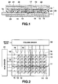
- FIG. 1 is a cross-sectional view of a display device according to the first embodiment.
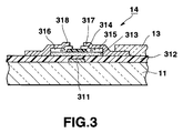
- FIG. 2 is a plan view of a transparent substrate on which pixel electrodes and active elements are formed.
- This display device is of an active matrix type, and comprises a pair of transparent substrates (e.g., glass substrates) 11 and 12, a liquid crystal 21 provided between the transparent substrates 11 and 12, and a pair of polarization plates 23 and 24 arranged to sandwich those substrates 11 and 12, as shown in FIG. 1.
- transparent substrates e.g., glass substrates
- liquid crystal 21 provided between the transparent substrates 11 and 12
- polarization plates 23 and 24 arranged to sandwich those substrates 11 and 12, as shown in FIG. 1.
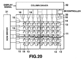
- transparent pixel electrodes 13 formed of a transparent conductive material like ITO (Indium Tin Oxide), and thin film transistors (TFTs) 14 having their source electrodes connected to the associated pixel electrodes 13 are arranged on the lower transparent substrate (hereinafter called lower substrate) 11 in a matrix form.
- ITO Indium Tin Oxide
- TFTs thin film transistors
- gate lines (scan lines) 15 are laid between the rows of pixel electrodes 13 and data lines (gradation signal lines) 16 are laid between the columns of pixel electrodes 13.
- the gate electrodes of the individual TFTs 14 are connected to the associated gate lines 15, and the drain electrodes of the TFTs 14 are connected to the associated data lines 16.
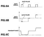
- each TFT 14 has a gate electrode 311 formed on the lower substrate 11, a gate insulator film 312 covering the entire lower substrate 11, an intrinsic semiconductor layer 313 formed on the gate insulator film 312, a blocking layer 314 formed on a channel region of the intrinsic semiconductor layer 313, contact layers 315 and 316 formed on a source region and a drain region of the intrinsic semiconductor layer 313, a source electrode 317 connected to the contact layer 315, and a drain electrode 318 connected to the contact layer 316.
- Connected to the source electrode 317 is the associated pixel electrode 13.
- the gate lines 15 are connected to a row driver 31, and the data lines 16 are connected to a column driver 32.
- the row driver 31 applies a gate voltage (which will be described later) to the gate lines 15 to scan the gate lines 15.
- the column driver 32 receives image data (gradation signal) and applies a data signal corresponding to the image data to the data lines 16.
- an opposing electrode (common electrode) 17 which opposes the individual pixel electrodes 13 on the lower substrate 11 and is to be applied with a reference voltage V0, is formed on the upper transparent substrate (hereinafter called upper substrate) 12.
- the opposing electrode 17 is a transparent electrode made of ITO or the like.
- Aligning films 18 and 19 are provided on the electrode-forming surfaces of the lower substrate 11 and the upper substrate 12.
- the aligning films 18 and 19 are homogeneous aligning films formed of an organic high molecular compound, such as polyimide, and having a thickness of about 25 to 35 nm.
- the aligning films in use have dispersion force esd of 30 to 50, and relatively weak polar force esp of about 3 to 20.
- At least one of the opposing surfaces of the aligning films 18 and 19 has undergone an aligning treatment, "rubbing," once in each of the opposite and parallel directions.
- the lower substrate 11 and the upper substrate 12 are adhered at their peripheral edge portions via a frame-shaped seal member 20, thus forming a liquid crystal (LC) cell 25.
- the gap between the aligning films 18 and 19 is regulated to a constant gap of 1.4 ⁇ m to 2.4 ⁇ m by the seal member 20 and a gap member 22.
- the liquid crystal 21 is sealed in an region surrounded by the substrates 11 and 12 and the seal member 20.
- the molecules of the liquid crystal 21 (hereinafter called LC molecules) have a single helical structure (in the case of an FLC) or a double helical structure (in the case of an AFLC) in a bulk state. Since the gap length of the LC cell 25 is shorter than the helical pitch, the molecules of the liquid crystal 21 are sealed in the LC cell 25 with the helix broken.
- the liquid crystal 21 is formed of a liquid crystal composition (FLC or AFLC) of a chiral smectic C phase or CA phase (SmC* or SmCA*) whose molecules have spontaneous polarizations Ps and have a cone angle 2 ⁇ which is twice the angle (tilt angle) defined by the axis of the cone drawn by the molecules and the cone is greater than 45° (desirably equal to or greater than 60°).
- FLC or AFLC liquid crystal composition
- SmC* or SmCA* a chiral smectic C phase or CA phase
- the homogeneous component (the component projected on a plane parallel to the major surfaces of the substrates 11 and 12) of the director of the liquid crystal 21 (the average aligning direction of the long axes of a plurality of LC molecules which constitute the liquid crystal) continuously varies in accordance with the applied voltage.
- liquid crystal having such a property is an AFLC which is obtained by mixing liquid crystal materials (I) to (III) having skeleton structures expressed by chemical formula 1 at a ratio of 20% by weight, 40% by weight and 40% by weight.
- Those liquid crystal compounds are AFLC compounds having a chiral terminal chain bonded to ether and optionally a phenyl ring subjected to fluorine reduction.
- An LCD device using such an AFLC compound reduces the threshold value of electric field induced transition of an AFLC, which prominently shows a precursor phenomenon. As a result, the liquid crystal 21 does not have a distinctive threshold value in the electro-optical characteristic.
- a liquid crystal having such a structure and property is characterized in that the potential energy barrier of an antiferroelectric phase and a ferroelectric phase is smaller than that of an ordinary AFLC, and the order of the ferroelectric phase is disturbed more easily with a greater phase transition precursor phenomenon, as compared with the ordinary AFLC.
- the phase transition precursor phenomenon is a phenomenon such that the transmittance of an LC element at the optical location shown in FIG. 4 rises before the occurrence of the phase transition from the antiferroelectric phase to the ferroelectric phase when the strength of an electric field to be applied to the LC molecules having the antiferroelectric phase is gradually increased.
- the increase in transmittance means that the LC molecules behave before phase transition.
- the behavior of the LC molecules before phase transition means that the potential energy barrier of the antiferroelectric phase and ferroelectric phase is small.
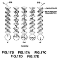
- Such an AFLC has a layer structure and a helical structure of aligned molecules in a bulk state; adjoining LC molecules has a double helical structure with helixes drawn by the LC molecules shifted by approximately 180° on an imaginary cone layer by layer, and the spontaneous polarizations of the LC molecules in adjoining smectic layers are canceled out each other.
- the AFLC liquid crystal sealed between the substrates 11 and 12 has a gap between the substrates (the cell gap of the LCD device 25) of about 1.5 ⁇ which is substantially equal to one pitch (natural pitch) of the helical structure of a liquid crystal. Therefore, the double helical structure of the LC molecules vanishes.
- the LC molecules of the antiferroelectric phase behaves along the imaginary cone in accordance with the strength of the electric field due to the small potential energy barrier of the antiferroelectric phase and ferroelectric phase. Accordingly, the homogeneous component of the director of the AFLC continuously varies in accordance with the applied voltage.
- a numeral "21C" indicates the direction of an aligning treatment performed on the aligning films 18 and 19.
- the molecules of the liquid crystal 21 are aligned with a normal line of a layer having a layer structure of a chiral smectic C phase or CA phase directed in the aligning treatment direction 21C within an error range of about ⁇ 2°.
- the liquid crystal 21 When a voltage lower than a negative predetermined voltage -VS is applied to the liquid crystal 21, the liquid crystal 21 becomes a first alignment state (ferroelectric phase) and the aligning directions of the LC molecules become substantially a first direction 21A. When a voltage higher than a positive predetermined voltage +VS is applied to the liquid crystal 21, the liquid crystal 21 becomes a second alignment state and the aligning directions of the LC molecules become substantially a second direction 21B. When a voltage of 0 V is to be applied to the liquid crystal 21, the average aligning direction of the LC molecules become substantially normal to the layer of the smectic phase of the liquid crystal, i.e., a direction 21C substantially between the first and second directions 21A and 21B (substantially the aligning treatment direction).
- the angle of deviation between the first direction 21A and the second direction 21B is equal to or greater than 45°, desirably equal to or greater than 50°, and more desirably equal to or greater than 60°.
- the transmission axis, 23A, of the polarization plate 23 should be set within an angular range defined by the first direction 21A and the aligning treatment direction 21C and should intersect the aligning treatment direction 21C at an angle of 45°/2.
- the transmission axis 23A is set in a direction of 22.5° with respect to the aligning treatment direction 21C.
- the transmission axis, 24A, of the polarization plate 24 is set substantially perpendicular to the transmission axis 23A of the polarization plate 23.
- optical axis transmission axis
- the transmission axis 23A of the polarization plate 23 and the first direction 21A are so set as to intersect each other at a half the angle obtained by subtracting 45° from the deviation angle 2 ⁇ .
- the transmission axis 23A of the polarization plate 23 and the first direction 21A should be set to intersect each other at an angle equal to or greater than 2.5°
- the transmission axis 23A of the polarization plate 23 and the first direction 21A should be set to intersect each other at an angle equal to or greater than 7.5°.
- the LCD device having the transmission axes 23A and 24A of the polarization plates 23 and 24 set as shown in FIG. 4 provides the lowest transmittance (the darkest display) when the average aligning direction of the LC molecules are set parallel to the transmission axis 23A of the polarization plate 23, and provides the highest transmittance (the brightest display) when the average aligning direction of the LC molecules are set in a direction 21D inclined by 45° to the transmission axis 23A of the polarization plate 23.
- the linearly polarized light which has passed the incident-side polarization plate 23 is hardly affected by the polarization effect of the liquid crystal 21 and passes the layer of the liquid crystal 21 as the linearly polarized light.
- the linearly polarized light which has passed the layer of the liquid crystal 21 is absorbed by the polarization plate 24 whose transmission axis 24A is set perpendicular to the polarization direction. The display therefore becomes darker.
- the polarization state of the linearly polarized light which has passed the incident-side polarization plate 23 is changed (circularly polarized or elliptically polarized) by the birifringence effect of the liquid crystal 21.
- the component parallel to the transmission axis 24A of the outgoing-side polarization plate 24 passes through the polarization plate 24. The display therefore becomes brightest.
- the polarized light is changed in accordance with the average aligning direction of the LC molecules by the birifringence effect matching each alignment state.
- the component parallel to the transmission axis 24A of the outgoing-side polarization plate 24 passes through the polarization plate 24. Therefore, the display shows the brightness that matches with the alignment state of the LC molecules.
- the LC molecules change their aligning directions in accordance with a voltage to be applied between the pixel electrodes 13 and the opposing electrode 17. As shown in FIG. 5, therefore, the transmittance of this LCD device continuously changes when a sawtooth-like voltage of a relatively low frequency (about 0.1 Hz) is applied between the pixel electrodes 13 and the opposing electrode 17.
- this LCD device is of an active matrix type, a voltage which keeps the liquid crystal 21 in any alignment state can be held even during a non-selection period. This LCD device can therefore ensure gradation display by changing the transmittance.
- the transmittance of this LCD device becomes minimum when the director of the liquid crystal 21 is parallel to the transmission axis 23A of the polarization plate 23, and becomes maximum when that director intersects the transmission axis 23A at 45°. If this LCD device is used in an alignment state where the transmittance shows Tmin and Tmax, the liquid crystal 21 can be driven without being aligned in the first or second alignment state.
- the first and second alignment states are the states of a ferroelectric phase where all the molecules in the layer of the liquid crystal 21 are completely aligned in the same direction. In the state where the LC molecules show a ferroelectric phase, charges produced by the spontaneous polarization are apt to be held on the inner surfaces of the substrates 11 and 12. This makes the inversion of the LC molecules difficult, which makes it easier to cause burning.
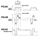
- FIG. 6A shows a gate signal to be applied to an arbitrary gate line 15 by the row driver 31, and FIG. 6B shows a data signal to be applied to each data line 16 by the column driver 32 in synchronism with the gate signal.
- the voltage of the data pulse is set to a voltage which does not set the liquid crystal 21 in a ferroelectric phase, or a voltage lying between VTmax and VTmin, and corresponds to a desired transmittance.
- FIG. 6C shows the transmittance of the LCD device for a pixel when the voltage of the data pulse shown in FIG. 6B is applied to the associated pixel electrode 13.
- the TFTs 14 in the selected row are turned on.
- a data signal corresponding to the display gradation and applied to each data line 16 by the column driver 32 is applied between the pixel electrodes 13 and the opposing electrode 17 via the enabled TFTs 14.
- the associated TFTs 14 are turned off.
- the voltage applied between the pixel electrodes 13 and the opposing electrode 17 is held in a pixel capacitor which is formed by the pixel electrodes 13, the opposing electrode 17 and the liquid crystal 21 located therebetween. Therefore, the display gradation corresponding to this held voltage is kept until the next selection period for this row as shown in FIG. 6C.
- This driving method can therefore cause the LCD device with the above-described structure to display an image of any gradation by controlling the voltage of the data pulse.
- the column driver 32 which accomplishes this driving method comprises a first sample and hold circuit 411, a second sample and hold circuit 412, an A/D (Analog/Digital) converter 413, a timing circuit 414 and a voltage converter 415, as shown in FIG. 7.
- A/D Analog/Digital
- the first sample and hold circuit 411 samples and holds a signal component (one image data) VD' for an associated pixel in externally supplied image data.
- the second sample and hold circuit 412 samples and holds a hold signal VD' output from the first sample and hold circuit 411.
- the A/D converter 413 performs A/D conversion on the hold signal VD' output from the second sample and hold circuit 412 to yield digital gradation data.
- the timing circuit 414 supplies a timing control signal indicating the sampling and holding operation to the first and second sample and hold circuits 411 and 412 in the selection period for each row.
- the voltage converter 415 converts the digital gradation data output from the A/D converter 413 to a data pulse having the associated voltage (the voltage for the drive system which is necessary to display the gradation indicated by the digital gradation data) VD, and sends the data pulse to the associated data line 16.
- This voltage converter 415 separates the power supply system in the signal processing system from the power supply system in the drive system.
- the output voltage VD of the voltage converter 415 is written in the pixel electrodes 13 to be applied to the liquid crystal 21 during the write period in which the TFTs 14 in the associated row are on. While the TFTs 14 are set off, the output voltage VD is held between the pixel electrodes 13 and the opposing electrode 17.
- the first sample and hold circuit 411, the second sample and hold circuit 412, the A/D converter 413 and the voltage converter 415 are arranged for each column of pixels, and the timing circuit 414 is provided in common to a plurality of columns.
- the structure of the column driver 32 which drive the LCD device by the driving method illustrated in FIGS. 6A-6C is not limited to the one shown in FIG. 7.
- a sample and hold circuit incorporated in the A/D converter 413 may be used as the second sample and hold circuit 412.
- the processed data may be supplied to the voltage converter 415 to be converted to a voltage for the drive system.
- the processed data may be temporarily converted to a gradation signal having a voltage for the signal processing system before being converted to a voltage for the drive system by the voltage converter.
- Various kinds of timing signals may be externally supplied to the column driver 32.
- Image data itself may be formed of digital data.
- the driving method shown in FIGS. 6A-6C does not permit the display gradation corresponding to the voltage of the data pulse to be specifically determined.
- another driving method as illustrated in, for example, FIGS. 8A through 8C should be employed.
- FIG. 8A shows a gate signal to be applied to an arbitrary gate line 15 by the row driver 31, and FIG. 8B shows a data signal to be applied to each data line 16 by the column driver 32 in synchronism with the gate signal.
- FIG. 8C shows the transmittance of the LCD device for a pixel when the voltage of the data signal shown in FIG. 8B is applied to the associated pixel electrode 13.
- the TFTs 14 in the selected row are turned on.
- a data pulse applied to each data line 16 by the column driver 32 is applied between the pixel electrodes 13 and the opposing electrode 17 via the enabled TFTs 14.
- the data pulse consists of a set pulse VH applied in a time slot t 1 for causing the LC molecules to be aligned in a predetermined alignment state, a reset pulse VL applied in a time slot t 2 for canceling the DC component of this set pulse, and a gradation pulse VD applied in a time slot t 3 and corresponding to the display gradation.
- the associated TFTs 14 are turned off.
- the voltage of the gradation pulse VD which has been applied between the pixel electrodes 13 and the opposing electrode 17 is held in a pixel capacitor which is formed by the pixel electrodes 13, the opposing electrode 17 and the liquid crystal 21 located therebetween.
- the display gradation corresponding to this held voltage is kept until the next selection period for this row.
- This driving method can therefore cause the LCD device with the above-described structure to display an image of any gradation by controlling the voltage of the data pulse.
- the application of the reset pulse VL can cancels out the unnecessary DC component to be applied to the liquid crystal 21. This relieves the storage of charges in the inner surfaces of the substrates 11 and 12, which makes the inversion of the LC molecules easier, and thus suppresses display burning.
- the column driver 32 which accomplishes this driving method comprises a first sample and hold circuit 421, a second sample and hold circuit 422, an A/D converter 423, a voltage data generator 424, a timing circuit 425, a multiplexer 426 and a voltage converter 427, as shown in FIG. 9.
- the first sample and hold circuit 421 samples and holds a signal component (one image data) VD' for an associated pixel in externally supplied image data.
- the second sample and hold circuit 422 samples and holds a hold signal VD' output from the first sample and hold circuit 421.
- the A/D converter 423 performs A/D conversion on the hold signal VD' output from the second sample and hold circuit 422 to yield digital gradation data DG.
- the voltage data generator 424 generates set pulse data DH corresponding to the set pulse VH and reset pulse data DL corresponding to the reset pulse VL.
- the timing circuit 425 supplies a timing control signal to the first and second sample and hold circuits 421 and 422 and enables timing signals T1, T2 and T3 respectively in time slots t 1, , t 2 and t 3 which constitutes the selection period (the period when the gate pulse is enabled) TS for each row.
- the multiplexer 426 selectively outputs the reset pulse data DL, the set pulse data DH and the digital gradation data DG from the A/D converter 423 in each selection period TS in response to the timing signals T1-T3 in order.
- the voltage converter 427 converts the output data of the multiplexer 426 to a high voltage for the drive system and sends the voltage to the associated data line 16. Specifically, the voltage converter 427 converts the reset pulse data to the reset pulse VL, the set pulse data to the set pulse VH and the digital gradation data to the write voltage VD for displaying gradation indicated by the image data, and sends the pulses and voltage to the associated data line 16. This voltage converter 427 separates the power supply system in the signal processing system from the power supply system in the drive system.
- the drive voltages VL, VH and VD output from the voltage converter 427 are written in the associated pixel electrodes 13 to be applied to the liquid crystal 21 in the respective time slots t 1 , t 2 and t 3 in the write period in which the TFTs 14 in the associated row are on. While the TFTs 14 are turned off, the write voltage VD applied at the timing t 3 is held between the pixel electrodes 13 and the opposing electrode 17.
- the first sample and hold circuit 421, the second sample and hold circuit 422, the multiplexer 426 and the voltage converter 427 are arranged for each column of pixels, and the timing circuit 425 and the voltage data generator 424 are commonly provided for a plurality of columns.
- the structure of the column driver 32 which drive the LCD device by the driving method illustrated in FIGS. 8A-8C is not limited to the one shown in FIG. 9.
- a sample and hold circuit incorporated in the A/D converter 423 may be used as the second sample and hold circuit 422.
- the processed data may be supplied to the multiplexer 426.
- the output data of the multiplexer 426 may be temporarily converted to a gradation signal having a voltage for the signal processing system before being converted to a voltage for the drive system by the voltage converter.
- Various kinds of timing signals may be externally supplied to the column driver 32.
- Image data itself may be formed of digital data.
- the reset pulse VL and the set pulse VH are equal in absolute value to each other but of the opposite polarities in the LCD device driving method illustrated in FIGS. 8A-8C
- the reset pulse VL may be set to a voltage which is equal to, but of the opposite polarity, the sum of the voltages of the set pulse VH and the gradation pulse VD.
- VL may be the set pulse
- VH may be the reset pulse.
- the reset pulse VL, set pulse VH and write pulse VD are sequentially applied in the write period TS in which the individual TFTs 14 are on, only the set pulse VH and the write pulse VD may be applied.
- the first to third time slots t 1 -t 3 need not be of the same length, but may have different lengths.
- the display gradation corresponding to the voltage of the data pulse can be specifically determined by the driving method shown in FIGS. 8A-8C.
- display burning may be caused by the DC component of the image signal corresponding to the data pulse.
- the reset pulse VL is set to a voltage which is equal to, but of the opposite polarity, the sum of the voltages of the set pulse VH and the gradation pulse VD, the voltage of the reset pulse may become too large so that the liquid crystal 21 exhibits a ferroelectric phase.
- a compensation pulse -VD whose voltage is equal in absolute value to the voltage of the write pulse VD but of the opposite polarity should be applied in a time slot t 0 prior to the application of the reset pulse VL, as shown in FIGS. 10A through 10C.
- the application order of the reset pulse VL and the compensation pulse -VD may be reversed.
- the column driver 32 which accomplishes this driving method differs from the column driver 32 shown in FIG. 9 in the structures of an A/D converter 423', a voltage data generator 424', a timing circuit 425' and a multiplexer 426'.
- the A/D converter 423' performs A/D conversion on the hold signal VD' output from the second sample and hold circuit 422 to yield digital gradation data DG. Further, the A/D converter 423' outputs compensation data -DG which is equal in absolute value to, but of the opposite polarity, the digital gradation data DG.
- the timing circuit 425' supplies a timing control signal to the first and second sample and hold circuits 421 and 422 and enables timing signals T0, T1, T2 and T3 respectively in four time slots t 0 , t 1, , t 2 and t 3 which constitutes the selection period (the period when the gate pulse is enabled) TS for each row.
- the multiplexer 426' sequentially selects and outputs the compensation data DG from the A/D converter 423', the reset pulse data DL, the set pulse data DH and the digital gradation data DG from the A/D converter 423' in each selection period TS in response to the timing signals T1-T3.
- an image with arbitrary gradation can be displayed without setting the liquid crystal 21 in a ferroelectric phase by continuously changing the gradation.
- the directions of the spontaneous polarizations PS of the LC molecules are matched each other, so that display burning is likely to occur.
- the spontaneous polarizations PS are not completely matched each other. Therefore, display burning does not easily occur and a high-grade image can be displayed.
- the LCD device uses a liquid crystal of a chiral smectic phase having spontaneous polarization SP is used as the liquid crystal 21, the response speed is fast and the angle of visibility is wide.
- the LCD device of the first embodiment can be driven by a DC voltage.
- a single voltage is applied for a single gradation unlike in the case of AC driving where two voltages of different polarities are applied for a single gradation. This can suppress the occurrence of flickering.
- the LCD device of the first embodiment is driven by the driving method illustrated in FIGS. 8A-8C or FIGS. 10A-10C, the molecules of the liquid crystal 21 are aligned substantially in a constant state by the set pulse VH which is applied in the time slot t 2 . Even when there is a hysteresis in the electro-optical characteristic of the liquid crystal 21, the display gradation corresponding to the gradation pulse VD can be determined specifically.
- the LCD device is driven by the driving method illustrated in FIGS. 10A-10C, in particular, the DC component of the gradation pulse can also be canceled. Even in the case where a bright image or a dark image is kept displayed, therefore, display burning can be prevented.
- the LCD device according to the first embodiment is not limited to the above-described structures, but may be modified in various other forms.
- the liquid crystal it is possible to set a liquid crystal not in a ferroelectric phase even when the liquid crystal is driven within an angular range smaller than the maximum angular range where the director of the liquid crystal is changed by the electric field.
- the driving can be accomplished within the angular range where the fluctuation angle of the director of the liquid crystal does not reach 45°. In this case, however, the maximum transmittance and the minimum transmittance cannot be obtained.
- the liquid crystal should be driven with the fluctuation angle of 45° in the range that does not provide a ferroelectric phase.
- the transmission axis of one of the polarization plates can be set in any direction, excluding the direction of the director which provides a ferroelectric phase within the range of the deviation angle 2 ⁇ of the liquid crystal which is greater than 45°.
- the transmission axis 23A of the polarization plate 23 may be set at the position of 12.5° from the first direction 21A, the transmission axis 24A of the polarization plate 24 may be set perpendicular or parallel to the transmission axis 23A, and the liquid crystal 21 may be driven with its director lying between the direction of the transmission axis 23A and a direction inclined by 45° to that direction.
- a liquid crystal having a deviation angle 2 ⁇ of 90° or greater may be used.
- the transmission axis 23A of the polarization plate 23 may be set normal to the smectic layer while setting the transmission axis 24A of the polarization plate 24 perpendicular or parallel to the transmission axis 23A.
- the liquid crystal 21 is sealed in the LC cell 25 with its helical structure broken in the first embodiment, the liquid crystal 21 may be sealed in the LC cell 25 with the helical structure.
- a liquid crystal having the basic structure as indicated by the chemical formula 1 can be used.
- a DHF liquid crystal having a cone angle 2 ⁇ of 45° or greater may be used as the liquid crystal 21.
- the DHF liquid crystal whose helical pitch is sufficiently smaller than the gap between the substrates and which has spontaneous polarization and shows a ferroelectric phase, is sealed between the substrates 11 and 12 with the helical structure of the LC molecules maintained.
- the DHF liquid crystal When a voltage of one polarity whose absolute value is equal to or greater than a predetermined value is applied, the DHF liquid crystal becomes a first ferroelectric phase where the helix is broken, and the LC molecules are aligned substantially in the first direction 21A shown in FIG. 4. When a voltage of the other polarity whose absolute value is equal to or greater than a predetermined value is applied, the DHF liquid crystal becomes a second ferroelectric phase where the helix is broken, and the LC molecules are aligned substantially in the second direction 21B shown in FIG. 4.
- the helical structure drawn by the LC molecules is deformed in accordance with the applied voltage to set an intermediate alignment state in which the average direction of the long-axis directions of the LC molecules becomes any direction between the first direction 21A and the second direction 21B.
- the transmittance of even an LCD device using a DHF liquid crystal changes as shown in FIG. 5 if a pair of polarization plates are arranged as shown in FIG. 4 and the applied voltage is changed.
- the transmission axis 24A of the polarization plate 24 and the transmission axis 23A of the polarization plate 23 may be set parallel to each other. In this case, the bright and dark gradations of an image to be displayed are reversed.
- the absorption axes of the polarization plates 23 and 24 may be used instead of the transmission axes.
- AFLCs (1) to (3) having the properties as given on Table 1 were prepared with the liquid crystals shown by (I) to (III) in the chemical formula 1 as the basic compositions.
- the spontanious polarization (PS) and the tilt angle were measured at the temperature of 25 °C.
- LCD devices which had the structure as shown in FIGS. 1-4 and respectively used those AFLCs (1) to (3) were fabricated.
- the electro-optical characteristics of those LCD devices were measured as the LCD devices were driven by the driving methods which will be discussed below.
- the polarization plate 23 of the LCD device was arranged with its transmission axis 23A inclined by 22.5° to the line normal to the layer having a layer structure of a smectic phase (smectic layer), while the transmission axis 24A of the other polarization plate 24 was set perpendicular to the transmission axis 23A of the polarization plate 23.
- Example 1-1 the electro-optical characteristic of the LCD device was measured as the LCD device was driven as follows.
- FIGS. 12A through 14B show the transmittances of the LCD devices obtained in the first driving and the second driving by the above driving method.
- FIG. 12A shows the relationship between the applied voltage and the transmittance when the LCD device using the AFLC (1) as the liquid crystal 21 is driven in such a way that the liquid crystal does not exhibit a ferroelectric phase.
- FIG. 12B shows the relationship between the applied voltage and the transmittance when the LCD device using the AFLC (1) is driven in such a way that the liquid crystal exhibits a ferroelectric phase.
- FIG. 12B shows the electro-optical characteristic of the LCD device in the same voltage range as in FIG. 12A.
- FIG. 13A shows the relationship between the applied voltage and the transmittance when the LCD device using the AFLC (2) as the liquid crystal 21 is driven in such a way that the liquid crystal does not exhibit a ferroelectric phase.
- FIG. 13B shows the relationship between the applied voltage and the transmittance when the LCD device using the AFLC (2) is driven in such a way that the liquid crystal exhibits a ferroelectric phase.
- FIG. 13B shows the electro-optical characteristic of the LCD device in the same voltage range as in FIG. 13A.
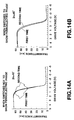
- FIG. 14A shows the relationship between the applied voltage and the transmittance when the LCD device using the AFLC (3) as the liquid crystal 21 is driven in such a way that the liquid crystal does not exhibit a ferroelectric phase.
- FIG. 14B shows the relationship between the applied voltage and the transmittance when the LCD device using the AFLC (3) is driven in such a way that the liquid crystal exhibits a ferroelectric phase.
- FIG. 14B shows the electro-optical characteristic of the LCD device in the same voltage range as in FIG. 14A.
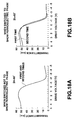
- the difference between the electro-optical characteristics in the first driving and the second driving is smaller in the case where the LCD device is driven so that the liquid crystal 21 does not exhibit a ferroelectric phase.
- the cone angle 2 ⁇ increases from 45°, to 50° then to 60°, the difference in the electro-optical characteristic of the liquid crystal 21 becomes smaller; with the cone angle 2 ⁇ equal to 60°, the difference in electro-optical characteristic almost completely disappears.
- Example 1-1 The same experiment as done on the Example 1-1 was conducted on the LCD device which uses, as the liquid crystal 21, a DHF liquid crystal having a cone angle 2 ⁇ of 61°, an ISO-SA transition temperature of 65.9°C, an SA-SC* transition temperature of 64.3°C, spontaneous polarization of 110 nc/cm 2 and a tilt angle ⁇ of 30.5°.
- the liquid crystal 21 a DHF liquid crystal having a cone angle 2 ⁇ of 61°, an ISO-SA transition temperature of 65.9°C, an SA-SC* transition temperature of 64.3°C, spontaneous polarization of 110 nc/cm 2 and a tilt angle ⁇ of 30.5°.
- Example 1-2 the electro-optical characteristic of the LCD device was measured as the LCD device was driven as follows.
- FIG. 15A shows the relationship between the applied voltage and the transmittance when the LCD device using the DHF liquid crystal having the aforementioned property as the liquid crystal 21 is driven in such a way that the liquid crystal does not exhibits a ferroelectric phase.
- FIG. 15B shows the relationship between the applied voltage and the transmittance when the LCD device using the DHF liquid crystal having the aforementioned property is driven in such a way that the liquid crystal exhibits a ferroelectric phase.
- FIG. 15B shows the electro-optical characteristic of the LCD device in the same voltage range as in FIG. 15A.
- Example 1-3 an LCD device using the AFLC (1) shown on Table 1 and used as the liquid crystal 21 in the Example 1-1 was fabricated.
- this LCD device was driven by the 1-pulse driving method and the 3-pulse driving method as follows with the selection period of 60 microseconds for each pixel at a duty ratio of 1/220.
- pulse voltages varying from +5 V to -5 V by 0.5 V were applied between the pixel electrodes 13 and the opposing electrode 17 in each selection period, and the transmittance for each pulse voltage was measured.
- pulse voltages varying in the reverse order from -5 V to +5 V by 0.5 V were applied between the pixel electrodes 13 and the opposing electrode 17, and the transmittance for each pulse voltage was measured.
- write pulse voltages were applied between the pixel electrodes 13 and the opposing electrode 17 after pulse voltages +5 V and -5 V were applied between the pixel electrodes 13 and the opposing electrode 17 each for 20 microseconds.
- the write pulse voltages were varied from -5V to +5V by 0.5 V, and the transmittance for each write pulse voltage was measured.
- write pulse voltages varying in the reverse order from -5 V to +5 V by 0.5 V were applied between the pixel electrodes 13 and the opposing electrode 17, after pulse voltages +5V and -5V were applied, and the transmittance for each write pulse voltage was measured.
- FIG. 16A sows the electro-optical characteristic of the LCD device driven by the 1-pulse driving method
- FIG. 16B sows the electro-optical characteristic of the LCD device driven by the 3-pulse driving method.
- the 1-pulse driving method generates a hysteresis.
- the 3-pulse driving method suppresses the influence of a hysteresis and can thus present stable gradation display.
- the structure of an LCD device according to the second embodiment is substantially the same as that of the LCD device according to the first embodiment which has been described above.
- the aligning films 18 and 19 are homogeneous aligning films which have undergone an aligning treatment of rubbing in the same direction (the third direction 21C in FIG. 4 as will be discussed later).
- the aligning films 18 and 19 exhibit alignment restriction force to attempt the alignment of the nearby LC molecules in the aligning treatment direction 21C.
- the aligning films 18 and 19 are formed of an organic high molecular compound, such as polyimide, and have undergone an aligning treatment like rubbing.
- the aligning films having dispersion force esd of 30 to 50, and relatively weak polar force esp of about 3 to 20 can be used.
- Used as the liquid crystal 21 is an AFLC having properties such that the potential energy barrier of an antiferroelectric phase and a ferroelectric phase is smaller than that of an ordinary AFLC, the order of the ferroelectric phase is disturbed more easily with a greater phase transition precursor phenomenon, as compared with the ordinary AFLC, and the mutual action of the individual five smectic layers is weak when the AFLC is sealed between the substrates.
- the liquid crystal 21 has a layer structure and a helical structure of aligned molecules in a bulk state; adjoining LC molecules has a double helical structure with helixes drawn by the LC molecules shifted by approximately 180° on an imaginary cone layer by layer, and the spontaneous polarizations of the LC molecules in adjoining smectic layers are canceled out each other.
- the layer thickness of the liquid crystal 21 (the cell gap of the LCD device 25) is about 1.5 ⁇ which is substantially equal to one pitch (natural pitch) of the helical structure of a liquid crystal material. Therefore, the double helical structure of the LC molecules vanishes.
- the liquid crystal 21 of the LCD device according to the second embodiment when sealed in the LC cell 25, is susceptible to the mutual action (interface effect) at the interface between the aligning films 18 and 19 or the influence of the alignment restriction force by the aligning treatment.
- the liquid crystal whose LC molecules are aligned without association between the smectic layers is in a phase where there is no relativity between layers when no electric field is applied, i.e., the direction of the director and the directions of spontaneous polarizations are at random.
- spontaneous polarizations are aligned in accordance with the electric field and their directions are inverted in accordance with the polarity of the applied voltage.
- FIGS. 17A through 17E show the responses on the molecular level when no electric field is applied to the liquid crystal whose LC molecules are aligned without association between the smectic layers and an electric field is applied.
- the long-axis directions and spontaneous polarizations of the LC molecules are not associated with each other between the smectic layers, and the director of the liquid crystal 21 substantially matches with the normal-line direction of the layer structure of the liquid crystal of a smectic phase.
- the relation among the direction of the aligning treatment performed on the aligning films 18 and 19, the transmission axes 23A and 24A of the polarization plates 23 and 24 and the aligning directions of the LC molecules is the same as the one in the first embodiment shown in FIG. 4.
- a change in the transmittance of the LCD device when a sawtooth-like voltage of a relatively low frequency (about 0.1 Hz) is applied between the pixel electrodes 13 and the opposing electrode 17 becomes substantially the same as the one in the first embodiment shown in FIGS. 6.
- this LCD device is of an active matrix type too, a voltage which keeps the liquid crystal 21 in any alignment state can be held even during a non-selection period. This LCD device can therefore ensure gradation display by changing the transmittance.
- the transmittance of this LCD device becomes minimum when the director of the liquid crystal 21 is parallel to the transmission axis 23A of the polarization plate 23, and becomes maximum when that director intersects the transmission axis 23A at 45°. If this LCD device is used in an alignment state where the transmittance shows Tmin and Tmax, the liquid crystal 21 can be driven without being aligned in the first or second alignment state.
- the first and second alignment states are the states of a ferroelectric phase where all the molecules in the layer of the liquid crystal 21 are completely aligned in the same direction. In the state where the LC molecules show a ferroelectric phase, charges produced by the spontaneous polarization are apt to be held on the inner surfaces of the substrates 11 and 12. This makes the inversion of the LC molecules difficult, which makes it easier to cause burning.
- the LCD device according to the second embodiment should also be driven by the driving method illustrated in FIGS. 6A-6C or the driving method illustrated in FIGS. 8A-8C both of the first embodiment.
- the column drivers 32 which accomplish those driving methods should be designed as those in the first embodiment which are shown in FIGS. 7 and 9.
- AFLCs (1) having the properties as given on Table 1 of the first embodiment were prepared with the liquid crystals shown by (I) to (III) in the chemical formula 1 as the basic compositions.
- LCD devices which had the structure as shown in FIGS. 1-4 and respectively used those AFLCs (1) were fabricated.
- the electro-optical characteristics of those fabricated LCD devices were measured as the LCD devices were driven by the same driving methods as employed for the Example 1-1.
- the polarization plate 23 of the LCD device was arranged with its transmission axis 23A inclined by 22.5° to the line normal to the layer having a layer structure of a smectic phase (smectic layer), while the transmission axis 24A of the other polarization plate 24 was set perpendicular to the transmission axis 23A of the polarization plate 23.
- FIGS. 18A and 18B show the transmittances of the LCD devices obtained in the first driving and the second driving by such a driving method.
- FIG. 18A shows the relationship between the applied voltage and the transmittance when the LCD device is driven in such a way that the liquid crystal does not exhibit a ferroelectric phase.
- FIG. 18B shows the relationship between the applied voltage and the transmittance when the LCD device is driven in such a way that the liquid crystal exhibits a ferroelectric phase.
- FIG. 18B shows the electro-optical characteristic of the LCD device in the same voltage range as in FIG. 18A.
- the first and second embodiments have been described with reference to the case where the LCD device is driven without consideration on a change in the temperature of the liquid crystal 21.
- the liquid crystal 21 has spontaneous polarization, however, the alignment state varies in accordance with a temperature change.
- the electro-optical characteristic of the liquid crystal 21 therefore varies in accordance with a temperature change, changing the gradation of an image to be displayed.
- FIG. 19 exemplifies a variation in electro-optical characteristic with a change in the temperature of the liquid crystal 21.
- the solid line shows the electro-optical characteristic when the temperature of the liquid crystal is the normal temperature (25 °C)
- the one-dot chain line indicates the electro-optical characteristic when the temperature of the liquid crystal is lower (10°C) than the normal temperature
- the two-dot chain line indicates the electro-optical characteristic when the temperature of the liquid crystal is higher (50°C) than the normal temperature.
- the director When the voltage VTmax at which the transmittance shows the maximum value is applied at the normal temparatuer, the director is directed to the 21D which intersects the direction of the transmission axis 23A of the polarization plate 23 approximately at 45°. Therefore, the director of the liquid crystal changes its direction by approximately 45° as the applied voltage is changed from VTmin to VTmax.
- a temperature sensor 33 is provided in the non-display area of the lower substrate 11 as shown in FIG. 20.
- the temperature sensor 33 indirectly detects the temperature of the liquid crystal 21 by sensing the temperature of the lower substrate 11.
- the temperature sensor 33 is connected to a controller 34 for temperature compensation of a data signal.
- the output signal of the controller 34 is supplied to the column driver 32.
- the structure of the column driver 32 differs from that in the first embodiment, as will be discussed later, to effect temperature compensation of the data signal from the controller 34.
- the temperature sensor 33 as shown in FIG. 21, comprises an intrinsic semiconductor layer 321 formed on a gate insulator film 312 and electrodes 324 and 325 connected to both end portions of the intrinsic semiconductor layer 321 via contact layers 322 and 323.
- the intrinsic semiconductor layers 313 and 321 are formed of amorphous silicon, polycrystalline silicon, monocrystalline silicon or the like which hardly contains an impurity.
- the contact layers 322 and 323 are formed of amorphous silicon, polycrystalline silicon, monocrystalline silicon or the like which is added with an n type impurity.
- the mobility of carriers in the intrinsic semiconductor layer 321 changes with the temperature. So does the substantial electrical resistivity of the intrinsic semiconductor layer 321. Accordingly, the temperature sensor 33 can detect the temperature by discriminating the resistance of the intrinsic semiconductor layer 321.
- the voltage of the data signal is adjusted in accordance with the temperature detected by the temperature sensor 33 in such a manner that the voltage VTmin which provides the transmittance Tmin in association with image data designating the lowest transmittance is applied to the liquid crystal 21, and the voltage VTmax which provides the transmittance Tmax in association with image data designating the highest transmittance is applied to the liquid crystal 21.
- the voltage of the data signal is adjusted in accordance with the temperature detected by the temperature sensor 33 in such a way that the director of the liquid crystal 21 is directed to a direction substantially matching with the direction of the transmission axis 23A of the polarization plate 23 in association with image data designating the lowest transmittance, and the director of the liquid crystal 21 is directed to the direction 21D intersecting the direction of the transmission axis 23A of the polarization plate 23 by approximately 45° in association with image data designating the highest transmittance.
- the voltage of the data signal to be applied to the liquid crystal is changed so that the director of the liquid crystal 21 which is aligned by one of the data signals associated with image data designating the lowest transmittance or image data designating the highest transmittance is set to be substantially coincident to either the direction of the transmission axis 23A of the polarization plate 23 or the direction 21D inclined by approximately 45° to the direction of the transmission axis 23A.
- the voltage variation range of the data signal to be applied is adjusted.
- FIG. 22 exemplifies the structure of the column driver 32 capable of adjusting the voltage of the data signal in accordance with the temperature. Like or same reference numerals are given to those components of the column driver 32 which are the same as the corresponding components of the column driver 32 in FIG. 7.
- This column driver 32 comprises a first sample and hold circuit 411, a second sample and hold circuit 412, an A/D converter 413, a timing circuit 414, a voltage converter 415 and a driver circuit 431.
- the column driver 32 shown in FIG. 22 differs from that shown in FIG. 7 in that the output signal VD'' of the voltage converter 415 is not applied to the data lines 16, but is supplied to the driver circuit 431.
- the driver circuit 43 comprised of an operational amplifier having a relatively large driving performance, amplifies the pulse signal VD'' and adds a bias voltage to the amplified signal to drive the data lines 16.
- the controller 34 sets the amplification factor ⁇ of the driver circuit 431 in accordance with an equation (1) and sets a bias voltage Vb in accordance with an equation (2).
- ⁇ A(1 + B(t - tr)/tr) where A and B are constants, t is the measuring temperature and tr is a reference temperature.
- Vb (VTmax(t) + VTmin(t))/2 where VTmax(t) is the applied voltage when the maximum gradation Tmax is acquired at the measuring temperature t and VTmin(t) is the applied voltage when the minimum gradation Tmin is acquired at the measuring temperature t.
- the constants A and B, and the applied voltages VTmax(t) and VTmin(t) should empirically be obtained and should be set in the controller 34 in advance.
- the output voltage VD'' of the voltage converter 415 is applied to the liquid crystal in the write period in which the TFTs 14 in the associated row are turned on through the driver circuit 431, and is held between the opposite electrodes 13 and 17 during the OFF duration of the TFTs 14.
- the first sample and hold circuit 411, the second sample and hold circuit 412, the A/D converter 413, the voltage converter 415 and the driver circuit 431 are arranged for each column of pixels, and the timing circuit 414 is commonly provided for a plurality of columns.
- the controller 34 adjusts the offset voltage and amplification factor of the driver circuit 431.
- the amplification factor ⁇ and the bias voltage Vb are adjusted in accordance with a temperature change so that the director of the liquid crystal 21 is set to substantially match with the transmission axis 23A of the polarization plate 23 at the time of displaying "black" of the lowest gradation and the director of the liquid crystal 21 is set to substantially match with the direction 21D at the time of displaying "white” of the highest gradation.
- the directors for the other gradations should be set to the desired respective positions.
- the LCD device driving method according to the third embodiment is the same as that of the first embodiment illustrated in FIGS. 6A-6C.
- the controller 34 adjusts the offset voltage and amplification factor of the driver circuit 431 in accordance with the temperature of the liquid crystal 21 that has been detected by the temperature sensor 33.
- the pulse voltage VD to be applied to the data lines 16 by the column driver 32 is therefore set in the light of changes in VTmin and VTmax caused by the temperature change of the liquid crystal 21.
- the director of the liquid crystal 21 is set substantially parallel to the direction of the transmission axis 23A of the polarization plate 23 regardless of the temperature. This can permit "black” of the lowest gradation to be displayed.
- the director of the liquid crystal 21 is set substantially parallel to the direction 21D which is inclined by 45° to the direction of the transmission axis 23A of the polarization plate 23 regardless of the temperature. Therefore, "white” of the highest gradation can be displayed.
- the LCD device according to the third embodiment can display "black” of the lowest gradation and "white” of the highest gradation and can thus display a clear image with high contrast.
- the display gradation corresponding to the voltage of the data pulse is not specifically determined by the driving method shown in FIGS. 6A-6C.
- another driving method as illustrated in FIGS. 8A through 8C, should be employed as per the first embodiment.
- the circuit structure of the column driver 32 which drives the LCD device by the driving method illustrated in FIGS. 8A-8C is illustrated in FIG. 23.
- This column driver 32 comprises a first sample and hold circuit 421, a second sample and hold circuit 422, an A/D converter 423, a voltage data generator 424, a timing circuit 425, a multiplexer 426, a voltage converter 427 and a driver circuit 441.
- the column driver 32 shown in FIG. 23 differs from that shown in FIG. 9 in that the output signal of the voltage converter 427 is not applied to the data lines 16, but is supplied to the driver circuit 441.
- the driver circuit 441 controls the voltage of the gradation pulse VD under the control of the controller 34.
- the first sample and hold circuit 421, the second sample and hold circuit 422, the A/D converter 423, the multiplexer 426, the voltage converter 427 and the driver circuit 441 are arranged for each column of pixels, and the timing circuit 425 and the voltage data generator 424 are commonly provided for a plurality of columns.
- the controller 34 also adjusts the offset voltage and the amplification factor in accordance with the output of the temperature sensor 33. That is, the amplification factor ⁇ and the bias voltage Vb are adjusted in accordance with a temperature change, so that the director of the liquid crystal is set to substantially match with the transmission axis 23A of the polarization plate 23 at the time of displaying "black" of the lowest gradation and the director of the liquid crystal is set to substantially match with the direction 21D at the time of displaying "white” of the highest gradation.
- the directors for the other gradations should be set to the desired respective positions.
- the display gradation corresponding to the gradation pulse VD is specifically determined.
- the LCD device according to the third embodiment can display a high-grade image without being affected by the temperature change.
- the spontaneous polarizations PS are not completely aligned. This makes it difficult to cause display burning so that a high-quality image can be displayed.
- the LCD device uses a liquid crystal of a chiral smectic phase having spontaneous polarization PS as the liquid crystal 21, the response speed is fast and the angle of visibility is wide.
- the LCD device according to the third embodiment can be driven by a DC voltage too.
- a single voltage is applied for a single gradation unlike in the case of AC driving where two voltages of different polarities are applied for a single gradation. It is therefore possible to suppress the occurrence of flickering.
- Measuring the temperature of the liquid crystal and changing the voltage to be applied between the electrodes in accordance with a change in the temperature of the liquid crystal as in the third embodiment can be adapted to the LCD device of the second embodiment which uses a liquid crystal having its molecules aligned without association between the smectic layers.
- the voltage to be applied to the liquid crystal 21 is controlled in accordance with the result of the detection of the temperature of the liquid crystal 21 by the temperature sensor 33 to thereby adjust the control of the image to be displayed.
- the brightness of the image to be displayed may be detected and the detected brightness may be compared with the original brightness of the image to be displayed, so that the voltage to be applied to the liquid crystal 21 is controlled based on the comparison result.
- This scheme can also compensate for the contrast of the display image.
- This invention can use other liquid crystals having spontaneous polarization, like a liquid crystal having a skeleton structure expressed by a chemical formula 2.
- This invention may be adapted to a color LCD device in which color filters for selectively passing only the lights of individual wavelength components of red, green and blue are arranged in a predetermined order to display a full color image.
- This invention is not limited to an LCD device using TFTs as active elements, but may be adapted to an LCD device using other types of active elements, such as MIMs (Metal Insulator Metals).
- MIMs Metal Insulator Metals
- this invention may be adapted to a passive matrix type LCD device which has scan electrodes 71 and signal electrodes 72 arranged on the opposing surfaces of the opposing substrates 11 and 12 with the signal electrodes 72 lying perpendicular to the scan electrodes 71.
- This invention may also be adapted to an LCD device which is driven by a static driving scheme.
Landscapes
- Physics & Mathematics (AREA)
- Chemical & Material Sciences (AREA)
- Crystallography & Structural Chemistry (AREA)
- Engineering & Computer Science (AREA)
- General Physics & Mathematics (AREA)
- Nonlinear Science (AREA)
- Computer Hardware Design (AREA)
- Theoretical Computer Science (AREA)
- Optics & Photonics (AREA)
- Liquid Crystal (AREA)
- Mathematical Physics (AREA)
- Liquid Crystal Display Device Control (AREA)
Applications Claiming Priority (10)
| Application Number | Priority Date | Filing Date | Title |
|---|---|---|---|
| JP18169296 | 1996-06-24 | ||
| JP181692/96 | 1996-06-24 | ||
| JP186897/96 | 1996-06-28 | ||
| JP18689896 | 1996-06-28 | ||
| JP18689796 | 1996-06-28 | ||
| JP186898/96 | 1996-06-28 | ||
| JP21592396 | 1996-07-30 | ||
| JP215923/96 | 1996-07-30 | ||
| JP25528396A JP3424149B2 (ja) | 1996-09-06 | 1996-09-06 | 表示素子及び表示素子装置 |
| JP255283/96 | 1996-09-06 |
Publications (2)
| Publication Number | Publication Date |
|---|---|
| EP0816907A2 true EP0816907A2 (de) | 1998-01-07 |
| EP0816907A3 EP0816907A3 (de) | 1998-09-16 |
Family
ID=27528811
Family Applications (1)
| Application Number | Title | Priority Date | Filing Date |
|---|---|---|---|
| EP97110227A Withdrawn EP0816907A3 (de) | 1996-06-24 | 1997-06-23 | Flüssigkristallanzeigevorrichtung |
Country Status (4)
| Country | Link |
|---|---|
| US (1) | US6163360A (de) |
| EP (1) | EP0816907A3 (de) |
| KR (1) | KR100237853B1 (de) |
| TW (1) | TW386174B (de) |
Cited By (2)
| Publication number | Priority date | Publication date | Assignee | Title |
|---|---|---|---|---|
| US7348953B1 (en) | 1999-11-22 | 2008-03-25 | Semiconductor Energy Laboratory Co., Ltd. | Method of driving liquid crystal display device |
| US7535448B2 (en) | 2001-02-08 | 2009-05-19 | Semiconductor Energy Laboratory Co., Ltd. | Liquid crystal display device, and method of driving the same |
Families Citing this family (14)
| Publication number | Priority date | Publication date | Assignee | Title |
|---|---|---|---|---|
| US20010052885A1 (en) * | 1997-09-12 | 2001-12-20 | Masaya Okita | Method for driving a nematic liquid crystal |
| JP2000338518A (ja) * | 1999-06-01 | 2000-12-08 | Nec Corp | 液晶表示装置および液晶表示装置の製造方法 |
| JP3918399B2 (ja) * | 2000-04-28 | 2007-05-23 | 富士通株式会社 | 液晶素子 |
| US6351327B1 (en) * | 2000-05-30 | 2002-02-26 | Agilent Technologies, Inc. | Liquid crystal pixel current sensing for silicon micro displays |
| JP2002244202A (ja) * | 2001-02-14 | 2002-08-30 | Sony Corp | 液晶プロジェクタ装置および液晶プロジェクタ装置の駆動方法 |
| JP2005539252A (ja) * | 2002-09-16 | 2005-12-22 | コーニンクレッカ フィリップス エレクトロニクス エヌ ヴィ | 表示装置 |
| US20060007248A1 (en) * | 2004-06-29 | 2006-01-12 | Damoder Reddy | Feedback control system and method for operating a high-performance stabilized active-matrix emissive display |
| JP4332515B2 (ja) * | 2004-04-28 | 2009-09-16 | キヤノン株式会社 | 液晶表示装置 |
| JP4654070B2 (ja) * | 2004-06-17 | 2011-03-16 | シチズンホールディングス株式会社 | 液晶表示装置及びメモリ性液晶パネルの駆動回路 |
| US8188958B2 (en) * | 2004-10-12 | 2012-05-29 | Samsung Electronics Co., Ltd. | Method, device and system of response time compensation |
| JP2009516229A (ja) * | 2005-11-16 | 2009-04-16 | ポリマー、ビジョン、リミテッド | 強誘電薄膜トランジスタに基づくピクセルを有するアクティブマトリクスディスプレイをアドレス指定するための方法 |
| US8400387B2 (en) * | 2008-07-09 | 2013-03-19 | Citizen Holdings Co., Ltd. | Liquid crystal display device |
| CN105533984B (zh) * | 2016-02-04 | 2018-02-02 | 温州乔盛皮革五金有限公司 | 一种可限重的行李箱把手以及设有所述把手的行李箱 |
| US11036091B2 (en) * | 2018-11-20 | 2021-06-15 | Himax Display, Inc. | Display panel |
Citations (1)
| Publication number | Priority date | Publication date | Assignee | Title |
|---|---|---|---|---|
| EP0686956A2 (de) | 1994-06-10 | 1995-12-13 | Casio Computer Co., Ltd. | Flüssigkristallanzeigegerät mit ferroelektrischer Phase und Verfahren zu ihrer Steuerung |
Family Cites Families (20)
| Publication number | Priority date | Publication date | Assignee | Title |
|---|---|---|---|---|
| US5255110A (en) * | 1985-12-25 | 1993-10-19 | Canon Kabushiki Kaisha | Driving method for optical modulation device using ferroelectric liquid crystal |
| JPS63226624A (ja) * | 1986-12-17 | 1988-09-21 | Canon Inc | 液晶素子 |
| JPH01288826A (ja) * | 1988-05-16 | 1989-11-21 | Ricoh Co Ltd | 強誘電性液晶素子 |
| JP2523811B2 (ja) * | 1988-09-02 | 1996-08-14 | 株式会社日立製作所 | 液晶光変調装置 |
| US5847790A (en) * | 1989-02-16 | 1998-12-08 | S.T. Lagerwall S.A.R.L. | Liquid crystal devices using a linear electro-optic effect |
| JP2827269B2 (ja) * | 1989-04-25 | 1998-11-25 | セイコーエプソン株式会社 | 液晶素子の駆動方法 |
| US5061044A (en) * | 1989-05-23 | 1991-10-29 | Citizen Watch Co., Ltd. | Ferroelectric liquid crystal display having opposingly inclined alignment films wherein the liquid crystal has one twisted and two aligned states which coexist and a driving method to produce gray scale |
| JPH03274090A (ja) * | 1990-03-23 | 1991-12-05 | Seiko Epson Corp | 液晶表示装置 |
| JP3033257B2 (ja) * | 1991-07-11 | 2000-04-17 | セイコーエプソン株式会社 | 液晶表示装置 |
| JPH0580101A (ja) * | 1991-09-25 | 1993-04-02 | Toshiba Corp | 電子機器自動調整装置 |
| JPH06289367A (ja) * | 1992-03-04 | 1994-10-18 | Shunsuke Kobayashi | 液晶表示装置 |
| JPH05297350A (ja) * | 1992-04-15 | 1993-11-12 | Idemitsu Kosan Co Ltd | 液晶光学素子用温度補償装置 |
| JPH05303081A (ja) * | 1992-04-24 | 1993-11-16 | Semiconductor Energy Lab Co Ltd | 液晶電気光学装置 |
| US5555110A (en) * | 1992-12-21 | 1996-09-10 | Semiconductor Energy Laboratory Company, Ltd. | Method of driving a ferroelectric liquid crystal display |
| JP3285402B2 (ja) * | 1993-01-14 | 2002-05-27 | シチズン時計株式会社 | 反強誘電性液晶パネル |
| US5781266A (en) * | 1993-09-27 | 1998-07-14 | Matsushita Electric Industrial Co., Ltd. | Ferroelectric liquid crystal display device and method for producing the same |
| JPH07311373A (ja) * | 1994-05-16 | 1995-11-28 | Citizen Watch Co Ltd | 反強誘電性液晶素子およびその駆動方法 |
| JPH07334130A (ja) * | 1994-06-10 | 1995-12-22 | Casio Comput Co Ltd | 強誘電性液晶表示装置及び強誘電性液晶表示素子の駆動方法 |
| JPH0854605A (ja) * | 1994-08-15 | 1996-02-27 | Citizen Watch Co Ltd | 反強誘電性液晶ディスプレイの駆動方法 |
| JP3136052B2 (ja) * | 1994-09-30 | 2001-02-19 | シャープ株式会社 | 強誘電性液晶素子 |
-
1997
- 1997-06-19 US US08/878,812 patent/US6163360A/en not_active Expired - Lifetime
- 1997-06-23 TW TW086108754A patent/TW386174B/zh not_active IP Right Cessation
- 1997-06-23 EP EP97110227A patent/EP0816907A3/de not_active Withdrawn
- 1997-06-24 KR KR1019970026721A patent/KR100237853B1/ko not_active Expired - Fee Related
Patent Citations (1)
| Publication number | Priority date | Publication date | Assignee | Title |
|---|---|---|---|---|
| EP0686956A2 (de) | 1994-06-10 | 1995-12-13 | Casio Computer Co., Ltd. | Flüssigkristallanzeigegerät mit ferroelektrischer Phase und Verfahren zu ihrer Steuerung |
Cited By (2)
| Publication number | Priority date | Publication date | Assignee | Title |
|---|---|---|---|---|
| US7348953B1 (en) | 1999-11-22 | 2008-03-25 | Semiconductor Energy Laboratory Co., Ltd. | Method of driving liquid crystal display device |
| US7535448B2 (en) | 2001-02-08 | 2009-05-19 | Semiconductor Energy Laboratory Co., Ltd. | Liquid crystal display device, and method of driving the same |
Also Published As
| Publication number | Publication date |
|---|---|
| TW386174B (en) | 2000-04-01 |
| EP0816907A3 (de) | 1998-09-16 |
| KR100237853B1 (ko) | 2000-01-15 |
| KR19980024066A (ko) | 1998-07-06 |
| US6163360A (en) | 2000-12-19 |
Similar Documents
| Publication | Publication Date | Title |
|---|---|---|
| US6163360A (en) | Liquid crystal display apparatus | |
| EP0632426B1 (de) | Flüssigkristallanzeigegerät und Steuerverfahren dafür | |
| US6046790A (en) | LCD device having relationship between spontaneous polarization and capacitance | |
| EP0176763A1 (de) | Flüssigkristallbauelement und Verfahren zu dessen Betrieb | |
| EP0554109B1 (de) | Verfahren zur Ansteuerung einer Flüssigkristall- Anzeigevorrichtung | |
| US6208403B1 (en) | Antiferroelectric liquid crystal display device | |
| US6091478A (en) | Liquid Crystal Display device using liquid crystal having ferrielectric phase between substrates and method for driving the same | |
| EP1897083A1 (de) | Verfahren zur ansteuerung einer flüssigkristallanzeigevorrichtung | |
| US6636193B1 (en) | Liquid crystal device | |
| US6323850B1 (en) | Driving method for liquid crystal device | |
| JP2003005151A (ja) | 液晶表示素子の駆動方法 | |
| US6175401B1 (en) | Liquid crystal display device having a liquid crystal layer which contains liquid crystal molecules in a plurality of alignment state and method for driving the same | |
| JP2984789B2 (ja) | 表示素子装置及び表示素子の駆動方法 | |
| US20100177027A1 (en) | Liquid crystal device and method of driving liquid crystal device | |
| US20030006954A1 (en) | Driving method for liquid crystal device | |
| JP2681528B2 (ja) | 液晶ライトバルブ装置 | |
| US6069602A (en) | Liquid crystal display device, liquid crystal display apparatus and liquid crystal driving method | |
| JP3424149B2 (ja) | 表示素子及び表示素子装置 | |
| JP3530767B2 (ja) | 液晶素子の駆動方法 | |
| EP1066544A2 (de) | Flüssigkristallanzeigevorrichtung | |
| JP2984788B2 (ja) | 表示素子装置及び表示素子の駆動方法 | |
| JP3039170B2 (ja) | 強誘電性液晶表示素子の駆動方法 | |
| JP2001255509A (ja) | スメクティック液晶光学装置 | |
| JPH03242624A (ja) | 液晶ライトバルブ装置 | |
| JP2940482B2 (ja) | 表示素子装置 |
Legal Events
| Date | Code | Title | Description |
|---|---|---|---|
| PUAI | Public reference made under article 153(3) epc to a published international application that has entered the european phase |
Free format text: ORIGINAL CODE: 0009012 |
|
| 17P | Request for examination filed |
Effective date: 19970715 |
|
| AK | Designated contracting states |
Kind code of ref document: A2 Designated state(s): DE FR GB NL |
|
| RAP1 | Party data changed (applicant data changed or rights of an application transferred) |
Owner name: CASIO COMPUTER CO., LTD. |
|
| PUAL | Search report despatched |
Free format text: ORIGINAL CODE: 0009013 |
|
| AK | Designated contracting states |
Kind code of ref document: A3 Designated state(s): AT BE CH DE DK ES FI FR GB GR IE IT LI LU MC NL PT SE |
|
| AKX | Designation fees paid |
Free format text: DE FR GB NL |
|
| RBV | Designated contracting states (corrected) |
Designated state(s): DE FR GB NL |
|
| 17Q | First examination report despatched |
Effective date: 20070821 |
|
| STAA | Information on the status of an ep patent application or granted ep patent |
Free format text: STATUS: THE APPLICATION IS DEEMED TO BE WITHDRAWN |
|
| 18D | Application deemed to be withdrawn |
Effective date: 20140103 |