EP0817262A2 - Cadre de connexion composite - Google Patents
Cadre de connexion composite Download PDFInfo
- Publication number
- EP0817262A2 EP0817262A2 EP97109589A EP97109589A EP0817262A2 EP 0817262 A2 EP0817262 A2 EP 0817262A2 EP 97109589 A EP97109589 A EP 97109589A EP 97109589 A EP97109589 A EP 97109589A EP 0817262 A2 EP0817262 A2 EP 0817262A2
- Authority
- EP
- European Patent Office
- Prior art keywords
- lead frame
- heat spreader
- heat
- connection
- heat distributor
- Prior art date
- Legal status (The legal status is an assumption and is not a legal conclusion. Google has not performed a legal analysis and makes no representation as to the accuracy of the status listed.)
- Withdrawn
Links
Images
Classifications
-
- H—ELECTRICITY
- H10—SEMICONDUCTOR DEVICES; ELECTRIC SOLID-STATE DEVICES NOT OTHERWISE PROVIDED FOR
- H10W—GENERIC PACKAGES, INTERCONNECTIONS, CONNECTORS OR OTHER CONSTRUCTIONAL DETAILS OF DEVICES COVERED BY CLASS H10
- H10W40/00—Arrangements for thermal protection or thermal control
- H10W40/70—Fillings or auxiliary members in containers or in encapsulations for thermal protection or control
- H10W40/77—Auxiliary members characterised by their shape
- H10W40/778—Auxiliary members characterised by their shape in encapsulations
-
- H—ELECTRICITY
- H10—SEMICONDUCTOR DEVICES; ELECTRIC SOLID-STATE DEVICES NOT OTHERWISE PROVIDED FOR
- H10W—GENERIC PACKAGES, INTERCONNECTIONS, CONNECTORS OR OTHER CONSTRUCTIONAL DETAILS OF DEVICES COVERED BY CLASS H10
- H10W70/00—Package substrates; Interposers; Redistribution layers [RDL]
- H10W70/40—Leadframes
- H10W70/421—Shapes or dispositions
Definitions
- the invention relates to a lead frame for use in a Power semiconductor component. This is for distribution and deriving those arising in the electronic component Heat associated with a heat spreader that is at least partially is integrated into a plastic housing.
- connection legs are bendable and solderable have to be.
- the material thickness of the also as system carrier designated lead frame is, for example, 0.25 mm.
- the material thickness of the heat spreader is, for example at 1.3 mm.
- heat spreader before spraying and heat sink are present. This is done in manufacturing achieved a variety of lead frames in a row different processing stations in a coherent volume is fed. Corresponding to this will be to the central part of everyone called the island Ladder frame applied structured semiconductor elements and electrically connected within the lead frame. The supply and attachment of a heat spreader must in production also successively on each unit of leadframe and chip happen, using heat spreader and lead frame should be connected. After making a lead frame, i.e. a metal strip, with very different strengths in different places heat sink and lead frame are complex or impossible be composed of two components.
- the invention has for its object a lead frame to provide with heat distributors, the island the lead frame ensures good heat dissipation and at the same time reliable and permanent electrical with ground connected is.
- the invention leads to the success that the system carrier or Ladder frame with the heat spreader for heat dissipation the operating heat generated in a semiconductor element serves reliably assembled by a welded joint can be.
- the heat spreader due to the heat development of the semiconductor chip is a technical solution for the production of the mechanical Stability of the arrangement of the lead frame and semiconductor chip Tobe offered.
- the use of a composite Head frame in which the heat spreader as Island installed becomes inevitable.
- the island must be provided by the heat spreader the ground contact with a connection leg, which for the Ground contact is used, reliably connected.
- the island or the heat distributor is connected by means of a Welded connection connected to the lead frame.
- this welded connection can be made by a Laser welding can be represented.
- the lead frame and heat spreader may be large put together so that there are enough places result in overlapping areas where a weld can be produced is.
- the peculiarity is in both cases the production of a fillet weld joint, wherein the parts to be connected lie flat against each other and the face of the thinner metal strip, in this case of the lead frame, on the flat side of the heat distributor is welded on.
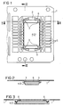
- Figure 1 shows a lead frame (leadframe assembly).
- a structured lead frame 1 is shown, that in production in a multitude is provided in a metal strip.
- a heat spreader 2 is added to each lead frame 1.
- a crimp connection for example.
- the lead frame 1 and the heat spreader 2 via a Welded joint 2, in particular a laser welded joint, connected to each other in several places.
- the lead frame 1 has a centrally positioned integrated island 4 on, which serves to hold the semiconductor element and by the heat spreader 2 is shown.
- FIGS. 2 and 3 show the corresponding sectional representations from FIG. 1.
- the heat distributor 2 representing the island 4 is shown.
- the lead frame 1 shown in section shows a so-called. downset ", whereby the web 6 is lowered.
- the cutouts 3 are also visible in FIG. 2, within which the lead frames 1 and the heat distributor 2 are connected by means of laser welding.
- FIG. 3 shows a sectional view rotated by 90 ° with respect to FIG again the webs 6 can be seen with which the lead frame 1 lies against one another with the heat spreader 2.
- the heat distributor 2 necessary for power semiconductor elements is shown, is reliably connected to ground.
- the material thickness of the components is, for example the lead frame 1 0.25 mm and for the heat spreader 2 1.3 mm.
- the particular advantages of a laser welded joint are in that no deformations of the lead frame 1 are expected and that there is a firm connection, for example withstands a pulling force of 40 N.
- the places where a welded joint is created can be even over an area or evenly over the circumference of the Island of the heat distributor or in particularly exposed areas to be ordered. With a laser beam you can also through-welding in the case of superimposed joints Generate metal strips. Leave with a laser beam themselves on front sides that are on the other connection partner lie on or adjoin in any form, fillet-like Generate welds.
- recesses 3 within the lead frame 1 can be provided in which the two connection partners be welded. These recesses 3 that here are represented as circles, can take any shape.
- the advantage is still achieved that on the island surface an otherwise necessary silver layer can be omitted.
- This silver layer is partially necessary, for example riveted island electrically by means of a bonding wire connect to.
- the saving of the silver layer results Cost savings and also improves an adhesive bond between semiconductor element (not shown here) and the Island 4.
- the creation of ground contact is after as before.
- a silver spot is a silver job suitable form, for example an electrical connection between the semiconductor element and the lead frame or one To manufacture part of it.
- connection between lead frame 1 and heat spreader 2 shows a uniform structure for a semiconductor arrangement with appropriate heat dissipation with simultaneous internal electrical connection.
- a recess 3 can, for example, be shown in the form of a slot are with the dimensions 0.25 mm x 2 mm.
- the focused one Laser beam is aimed at the center of the slot, with on two narrow sides of the lead frame 1 within the recess 3 a welded connection can be produced.
- the laser can be used universally and can consistently stable connections with high Strength values generate when different absorption ratios at different points on a workpiece not to different coupling of the laser power to lead.
- a laser welding process is always available and offers economic advantages.
Landscapes
- Lead Frames For Integrated Circuits (AREA)
Applications Claiming Priority (2)
| Application Number | Priority Date | Filing Date | Title |
|---|---|---|---|
| DE19625384 | 1996-06-25 | ||
| DE19625384A DE19625384A1 (de) | 1996-06-25 | 1996-06-25 | Zusammengesetzter Leiterrahmen |
Publications (2)
| Publication Number | Publication Date |
|---|---|
| EP0817262A2 true EP0817262A2 (fr) | 1998-01-07 |
| EP0817262A3 EP0817262A3 (fr) | 1999-07-07 |
Family
ID=7797953
Family Applications (1)
| Application Number | Title | Priority Date | Filing Date |
|---|---|---|---|
| EP97109589A Withdrawn EP0817262A3 (fr) | 1996-06-25 | 1997-06-12 | Cadre de connexion composite |
Country Status (3)
| Country | Link |
|---|---|
| EP (1) | EP0817262A3 (fr) |
| JP (1) | JPH1065084A (fr) |
| DE (1) | DE19625384A1 (fr) |
Families Citing this family (6)
| Publication number | Priority date | Publication date | Assignee | Title |
|---|---|---|---|---|
| EP1068640A1 (fr) | 1998-04-06 | 2001-01-17 | Infineon Technologies AG | Utilisation de la propriete structurale d'un composant electronique comme reference lors du positionnement du composant |
| DE19844873C2 (de) * | 1998-09-30 | 2003-11-13 | Possehl Electronic Gmbh | Trägeranordnung zur Aufnahme eines Halbleiterelements und Verfahren zur Herstellung einer Laser-Schweißverbindung |
| DE10117889A1 (de) | 2001-04-10 | 2002-10-24 | Osram Opto Semiconductors Gmbh | Leiterrahmen und Gehäuse für ein strahlungsemittierendes Bauelement, strahlungsemittierendes Bauelement sowie Verfahren zu dessen Herstellung |
| DE10117890B4 (de) * | 2001-04-10 | 2007-06-28 | Osram Opto Semiconductors Gmbh | Verfahren zum Herstellen eines strahlungsempfangenden und/oder -emittierenden Halbleiterbauelements und strahlungsempfangendes und/oder -emittierendes Halbleiterbauelement |
| JP4764983B2 (ja) * | 2006-07-25 | 2011-09-07 | 富士電機株式会社 | 半導体装置の製造方法 |
| JP7690357B2 (ja) * | 2020-12-02 | 2025-06-10 | 新光電気工業株式会社 | リードフレーム、半導体装置及びリードフレームの製造方法 |
Family Cites Families (7)
| Publication number | Priority date | Publication date | Assignee | Title |
|---|---|---|---|---|
| FR2116353B1 (fr) * | 1970-10-19 | 1976-04-16 | Ates Componenti Elettron | |
| JPH01215029A (ja) * | 1988-02-24 | 1989-08-29 | Hitachi Ltd | 半導体装置の製造方法 |
| DE4017697C2 (de) * | 1990-06-01 | 2003-12-11 | Bosch Gmbh Robert | Elektronisches Bauelement, Verfahren zu dessen Herstellung und Verwendung |
| IT1250405B (it) * | 1991-01-31 | 1995-04-07 | Sgs Thomson Microelectronics | Piastrina metallica di dissipazione del calore di un dispositivo a semiconduttore di potenza incapsulato in resina fornita di rilievi per la saldatura dei fili di massa |
| IT1252136B (it) * | 1991-11-29 | 1995-06-05 | St Microelectronics Srl | Struttura di dispositivo a semiconduttore con dissipatore metallico e corpo in plastica, con mezzi per una connessione elettrica al dissipatore di alta affidabilita' |
| US5220195A (en) * | 1991-12-19 | 1993-06-15 | Motorola, Inc. | Semiconductor device having a multilayer leadframe with full power and ground planes |
| DE19544347A1 (de) * | 1995-11-28 | 1997-06-05 | Siemens Ag | Verfahren zur Herstellung eines elektronischen Leistungsbauelementes und Leistungshalbleiterelement |
-
1996
- 1996-06-25 DE DE19625384A patent/DE19625384A1/de not_active Withdrawn
-
1997
- 1997-06-12 EP EP97109589A patent/EP0817262A3/fr not_active Withdrawn
- 1997-06-20 JP JP9180797A patent/JPH1065084A/ja not_active Withdrawn
Also Published As
| Publication number | Publication date |
|---|---|
| DE19625384A1 (de) | 1998-01-02 |
| EP0817262A3 (fr) | 1999-07-07 |
| JPH1065084A (ja) | 1998-03-06 |
Similar Documents
| Publication | Publication Date | Title |
|---|---|---|
| DE102007056750B4 (de) | Montageanordnung für eine Elektronische Steuervorrichtung und Steuervorrichtung damit | |
| DE102009055691B4 (de) | Leistungshalbleitermodul | |
| DE102014104399B4 (de) | Halbleiterchipgehäuse umfassend einen Leadframe | |
| DE69525868T2 (de) | Elektrische Verbindungsstruktur | |
| DE3009295A1 (de) | Halbleiterbaustein | |
| DE102008023457A1 (de) | Elektronische Steuervorrichtung und Verfahren zum Herstellen einer elektronischen Steuervorrichtung | |
| DE4220966C2 (de) | Verfahren zum Herstellen einer Trägerplatte für elektrische Bauteile | |
| DE4446289C2 (de) | Verfahren zur Mikroverbindung von Kontaktelementen | |
| DE2813968A1 (de) | Halbleiteranordnung mit kontaktwarzen-anschluessen | |
| DE2937050A1 (de) | Flachpaket zur aufnahme von elektrischen mikroschaltkreisen und verfahren zu seiner herstellung | |
| DE19713936A1 (de) | Planarer Kohlenstoffkommutator mit Herstellungsverfahren | |
| DE2937051A1 (de) | Flachpaket zur aufnahme von elektrischen mikroschaltkreisen und verfahren zu seiner herstellung | |
| DE102014218389B4 (de) | Halbleitermodul | |
| EP0817262A2 (fr) | Cadre de connexion composite | |
| DE19535775C2 (de) | Verfahren zum elektrischen Verbinden eines Kontaktfeldes eines Halbleiterchips mit zumindest einer Kontaktfläche sowie danach hergestellte Chipkarte | |
| DE10103084B4 (de) | Halbleitermodul und Verfahren zu seiner Herstellung | |
| DE102021200017A1 (de) | Halbleitermodul und verfahren zum herstellen eines halbleitermoduls | |
| DE112020003541T5 (de) | Leistungshalbleitermodul | |
| DE102009016842A1 (de) | Leitungsgitter für Elektronikgehäuse und Herstellungsverfahren | |
| DE10359564B4 (de) | Verfahren zum Verbinden von Bauteilen | |
| DE69427865T2 (de) | Halbleiteranordnung mit einer Wärmesenke und Herstellungsverfahren der Wärmesenke | |
| EP0593986B1 (fr) | Procédé de soudage d'un corps semi-conducteur à un élément de support | |
| DE8709301U1 (de) | Elektrisches Bauteil mit Anschlußstiften | |
| DE19544347A1 (de) | Verfahren zur Herstellung eines elektronischen Leistungsbauelementes und Leistungshalbleiterelement | |
| DE19623134A1 (de) | Leiterrahmenbaugruppe für ein Halbleiterbauelement |
Legal Events
| Date | Code | Title | Description |
|---|---|---|---|
| PUAI | Public reference made under article 153(3) epc to a published international application that has entered the european phase |
Free format text: ORIGINAL CODE: 0009012 |
|
| AK | Designated contracting states |
Kind code of ref document: A2 Designated state(s): AT BE CH DE DK ES FI FR GB GR IE IT LI LU MC NL PT SE |
|
| PUAL | Search report despatched |
Free format text: ORIGINAL CODE: 0009013 |
|
| AK | Designated contracting states |
Kind code of ref document: A3 Designated state(s): AT BE CH DE DK ES FI FR GB GR IE IT LI LU MC NL PT SE |
|
| AKX | Designation fees paid | ||
| REG | Reference to a national code |
Ref country code: DE Ref legal event code: 8566 |
|
| STAA | Information on the status of an ep patent application or granted ep patent |
Free format text: STATUS: THE APPLICATION IS DEEMED TO BE WITHDRAWN |
|
| 18D | Application deemed to be withdrawn |
Effective date: 20000108 |