EP0817265A1 - Cadre conducteur d'un circuit integré et bo tier comprenant un tel cadre et un dissipateur de chaleur - Google Patents
Cadre conducteur d'un circuit integré et bo tier comprenant un tel cadre et un dissipateur de chaleur Download PDFInfo
- Publication number
- EP0817265A1 EP0817265A1 EP97110219A EP97110219A EP0817265A1 EP 0817265 A1 EP0817265 A1 EP 0817265A1 EP 97110219 A EP97110219 A EP 97110219A EP 97110219 A EP97110219 A EP 97110219A EP 0817265 A1 EP0817265 A1 EP 0817265A1
- Authority
- EP
- European Patent Office
- Prior art keywords
- lead frame
- heatslug
- fastening elements
- fasteners
- frame according
- Prior art date
- Legal status (The legal status is an assumption and is not a legal conclusion. Google has not performed a legal analysis and makes no representation as to the accuracy of the status listed.)
- Withdrawn
Links
Images


Classifications
-
- H—ELECTRICITY
- H10—SEMICONDUCTOR DEVICES; ELECTRIC SOLID-STATE DEVICES NOT OTHERWISE PROVIDED FOR
- H10W—GENERIC PACKAGES, INTERCONNECTIONS, CONNECTORS OR OTHER CONSTRUCTIONAL DETAILS OF DEVICES COVERED BY CLASS H10
- H10W70/00—Package substrates; Interposers; Redistribution layers [RDL]
- H10W70/40—Leadframes
- H10W70/421—Shapes or dispositions
- H10W70/424—Cross-sectional shapes
- H10W70/427—Bent parts
-
- H—ELECTRICITY
- H10—SEMICONDUCTOR DEVICES; ELECTRIC SOLID-STATE DEVICES NOT OTHERWISE PROVIDED FOR
- H10W—GENERIC PACKAGES, INTERCONNECTIONS, CONNECTORS OR OTHER CONSTRUCTIONAL DETAILS OF DEVICES COVERED BY CLASS H10
- H10W40/00—Arrangements for thermal protection or thermal control
- H10W40/70—Fillings or auxiliary members in containers or in encapsulations for thermal protection or control
- H10W40/77—Auxiliary members characterised by their shape
- H10W40/778—Auxiliary members characterised by their shape in encapsulations
Definitions
- the invention relates to a lead frame for use in a power housing with connecting fingers and fasteners.
- the invention further relates to a component for use in a power package for an integrated circuit with a heatslug and a lead frame, the connecting finger and fasteners for connection to the Has heatslug.
- Such lead frames which are also referred to as lead frames, are used in power packages for integrated circuits usually used in combination with a heatslug that usually consists of a metallic block and one better heat distribution in the housing and thus a better one Heat dissipation is used.
- the invention has for its object to provide a lead frame and a component of the type mentioned, which are easy to manufacture and allow the best possible use of space.
- the supply frame mentioned at the beginning designed so that the fastening means twice have angled fasteners so that an end region the fasteners opposite the lead frame is offset in parallel, the end portions of the fasteners are flat to produce a connection and one of the fasteners electrically conductive with one of the Connection finger is connected.
- the component mentioned at the beginning which includes a heatslug and a Has lead frame, will continue to solve the problem developed that the fastener angled twice Have fasteners, an end portion of the fasteners offset parallel to the lead frame is, the end portions of the fasteners for connection are flat with the heatslug and one of the fasteners electrically conductive with one of the connecting fingers is connected, this connection finger a ground connection for the heatslug.
- a stable attachment is also with three Fasteners or more than four fasteners conceivable.
- the arrangement of four is particularly favorable Fasteners in the corners of the lead frame.
- the double angled fasteners are in one Continuing education Z-shaped.
- the direct transitions of the double angled Fastening elements are rounded, not a real one To create a kink and to avoid material breakage.
- the flat trained end regions of the fasteners preferably designed for spot welding. Is conceivable also a rivet, adhesive or solder attachment.
- the lead frame has two opposite rows of connecting fingers on, with the fasteners attached to the other two attached to opposite sides of the lead frame are.
- DSO Direct Small Outline
- the lead frame is preferably designed for use in a DSO housing.
- the heatslug has protrusions on, the dimensions of the flat end regions of the Fasteners correspond.
- Projections are arranged in the corners of the heatslug.
- the projection is advantageously in one piece with the Heatslug trained, but not as thick as this one, so the Projection an upper edge or upper projection of the heatslug represents.
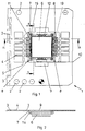
- FIG. 1 shows a lead frame according to the invention, which is denoted overall by 1.
- a lead frame is part of a strip that is usually consists of ten individual lead frames 1.
- the lead frame 1 has various circular recesses in the outer area 2 on that for the automated further transport of the serve entire strip with the plurality of lead frame 1.
- the elongated recesses 3 serve as a predetermined breaking point to separate the individual lead frames 1 from the entire strip.
- the lead frame 1 has two rows of each five connection fingers that face each other.
- the Connection fingers are designated 4.
- the stability of the connecting fingers 4 is through a connecting web 5, each connecting a series of connecting fingers increases.
- the connecting bridge 5 is after being pressed into a molding compound housing away.
- the connecting fingers 4 have a Silver coating 19, so that better contact making in the bond connection of the connecting fingers 4 with a Semiconductor chip is made possible.
- a heatslug 6 is arranged opposite the lead frame 1 is slightly lowered.
- the Heatslug 6 is from four fasteners 7 held, the connection attachment 8 to lead frame 1.
- a further recess 9 is provided so that one is dashed shown breaking edge 10 arises on the after pouring of an integrated circuit the outer area of the Lead frame 1 can be separated.
- One of the fasteners 7, in this case the one shown at the top left, has an electrical connection 11 which is integral with the connector 8 is formed and the closest Connection finger 4 contacted.
- a connecting finger 4 designed as a ground connection for the heatslug 6.
- the heatslug 6 is rectangular in shape and points to the extensions 12 on both ends.
- FIG. 2 shows a section along the line A-A from FIG. 1, which runs through one of the connecting fingers 4. Of the Cut through the connecting finger is from the elongated recess 3 and the hole 13 interrupted. In the central area of the lead frame, the contour of the recess 9 is indicated.
- the heatslug 6 is at a certain distance, also called downset, removed from the lead frame.
- the heatslug 6 has projections 14 at the corners, which are connected to the fastening element 7 are connected.
- the projections 14 are only formed over a fraction of the depth of the heatslug 6.
- the Fastening elements 7 are on the projections 14 Welding points 15 connected, which are also shown in Fig. 1 are. These welding spots are created with a laser.
- FIG. 3 shows a section along the line B-B in FIG. 1.
- the connecting fingers 4 are shown and in heatslug 6 a notch 16 is provided with which an additional anchoring of the heatslug is achieved when the housing is pressed in.
- connection attachment 8 on the level of the entire lead frame 1 is formed, a connecting part 17 and a flat end region 18.
- This extended areal End region 18 is offset parallel to the lead frame trained and with a weld spot 15 on the projection 14 of the heatslug 6 arranged, the projection 14 the corner area of the heatslug 6 expanded square and in its shape the flat expansion of the end region 18 of the fastening element 7 corresponds.
- Connecting part formed with two bends through which an overall Z-shaped fastener is created, which be formed in one piece. The bends can be used to protect the material is also rounded.
- the breaking edge 10 is to a parallel offset between connection attachment 8 and end area 18 .
Landscapes
- Lead Frames For Integrated Circuits (AREA)
Applications Claiming Priority (2)
| Application Number | Priority Date | Filing Date | Title |
|---|---|---|---|
| DE19626088 | 1996-06-28 | ||
| DE19626088 | 1996-06-28 |
Publications (1)
| Publication Number | Publication Date |
|---|---|
| EP0817265A1 true EP0817265A1 (fr) | 1998-01-07 |
Family
ID=7798368
Family Applications (1)
| Application Number | Title | Priority Date | Filing Date |
|---|---|---|---|
| EP97110219A Withdrawn EP0817265A1 (fr) | 1996-06-28 | 1997-06-23 | Cadre conducteur d'un circuit integré et bo tier comprenant un tel cadre et un dissipateur de chaleur |
Country Status (2)
| Country | Link |
|---|---|
| EP (1) | EP0817265A1 (fr) |
| JP (1) | JPH1065085A (fr) |
Cited By (2)
| Publication number | Priority date | Publication date | Assignee | Title |
|---|---|---|---|---|
| DE19844873A1 (de) * | 1998-09-30 | 2000-04-13 | Possehl Electronic Gmbh | Trägeranordnung zur Aufnahme eines Halbleiterelements |
| WO2007050038A1 (fr) * | 2005-10-25 | 2007-05-03 | Infineon Technologies Ag | Procede pour produire un boitier encapsule |
Families Citing this family (1)
| Publication number | Priority date | Publication date | Assignee | Title |
|---|---|---|---|---|
| CN107598324B (zh) * | 2017-10-23 | 2024-02-20 | 中国电子科技集团公司第四十三研究所 | 一种封装产品预热装置 |
Citations (10)
| Publication number | Priority date | Publication date | Assignee | Title |
|---|---|---|---|---|
| FR2487580A1 (fr) * | 1980-07-22 | 1982-01-29 | Thomson Csf Mat Tel | Dispositif semiconducteur a enrobage isolant comportant un dissipateur de chaleur apparent, et son procede de fabrication |
| GB2084796A (en) * | 1980-09-17 | 1982-04-15 | Hitachi Ltd | Mounting and cooling arrangements for semiconductor devices |
| JPS58219755A (ja) * | 1982-06-14 | 1983-12-21 | Nec Corp | 集積回路パツケ−ジ |
| EP0443508A1 (fr) * | 1990-02-22 | 1991-08-28 | STMicroelectronics S.r.l. | Cadre conducteur pour empaquetage de dispositifs de puissance intégrés |
| EP0503072A1 (fr) * | 1990-09-10 | 1992-09-16 | Fujitsu Limited | Dispositif a semi-conducteurs et son procede de fabrication |
| EP0588491A2 (fr) * | 1992-08-14 | 1994-03-23 | Texas Instruments Incorporated | Cadre de conducteur pour circuits intégrés et procédé pour améliorer la dissipation de chaleur |
| US5345106A (en) * | 1990-06-01 | 1994-09-06 | Robert Bosch Gmbh | Electronic circuit component with heat sink mounted on a lead frame |
| US5497032A (en) * | 1993-03-17 | 1996-03-05 | Fujitsu Limited | Semiconductor device and lead frame therefore |
| EP0712160A2 (fr) * | 1994-11-14 | 1996-05-15 | Texas Instruments Incorporated | Améliorations dans ou relatives à des circuits intégrés |
| JPH08125082A (ja) * | 1994-10-24 | 1996-05-17 | Sanyo Electric Co Ltd | リードフレームおよび半導体装置の製造方法 |
-
1997
- 1997-06-20 JP JP9180798A patent/JPH1065085A/ja active Pending
- 1997-06-23 EP EP97110219A patent/EP0817265A1/fr not_active Withdrawn
Patent Citations (10)
| Publication number | Priority date | Publication date | Assignee | Title |
|---|---|---|---|---|
| FR2487580A1 (fr) * | 1980-07-22 | 1982-01-29 | Thomson Csf Mat Tel | Dispositif semiconducteur a enrobage isolant comportant un dissipateur de chaleur apparent, et son procede de fabrication |
| GB2084796A (en) * | 1980-09-17 | 1982-04-15 | Hitachi Ltd | Mounting and cooling arrangements for semiconductor devices |
| JPS58219755A (ja) * | 1982-06-14 | 1983-12-21 | Nec Corp | 集積回路パツケ−ジ |
| EP0443508A1 (fr) * | 1990-02-22 | 1991-08-28 | STMicroelectronics S.r.l. | Cadre conducteur pour empaquetage de dispositifs de puissance intégrés |
| US5345106A (en) * | 1990-06-01 | 1994-09-06 | Robert Bosch Gmbh | Electronic circuit component with heat sink mounted on a lead frame |
| EP0503072A1 (fr) * | 1990-09-10 | 1992-09-16 | Fujitsu Limited | Dispositif a semi-conducteurs et son procede de fabrication |
| EP0588491A2 (fr) * | 1992-08-14 | 1994-03-23 | Texas Instruments Incorporated | Cadre de conducteur pour circuits intégrés et procédé pour améliorer la dissipation de chaleur |
| US5497032A (en) * | 1993-03-17 | 1996-03-05 | Fujitsu Limited | Semiconductor device and lead frame therefore |
| JPH08125082A (ja) * | 1994-10-24 | 1996-05-17 | Sanyo Electric Co Ltd | リードフレームおよび半導体装置の製造方法 |
| EP0712160A2 (fr) * | 1994-11-14 | 1996-05-15 | Texas Instruments Incorporated | Améliorations dans ou relatives à des circuits intégrés |
Non-Patent Citations (2)
| Title |
|---|
| PATENT ABSTRACTS OF JAPAN vol. 008, no. 070 (E - 235) 3 April 1984 (1984-04-03) * |
| PATENT ABSTRACTS OF JAPAN vol. 096, no. 009 30 September 1996 (1996-09-30) * |
Cited By (4)
| Publication number | Priority date | Publication date | Assignee | Title |
|---|---|---|---|---|
| DE19844873A1 (de) * | 1998-09-30 | 2000-04-13 | Possehl Electronic Gmbh | Trägeranordnung zur Aufnahme eines Halbleiterelements |
| DE19844873C2 (de) * | 1998-09-30 | 2003-11-13 | Possehl Electronic Gmbh | Trägeranordnung zur Aufnahme eines Halbleiterelements und Verfahren zur Herstellung einer Laser-Schweißverbindung |
| WO2007050038A1 (fr) * | 2005-10-25 | 2007-05-03 | Infineon Technologies Ag | Procede pour produire un boitier encapsule |
| US7674657B2 (en) | 2005-10-25 | 2010-03-09 | Infineon Technologies Ag | Method of manufacture of encapsulated package |
Also Published As
| Publication number | Publication date |
|---|---|
| JPH1065085A (ja) | 1998-03-06 |
Similar Documents
| Publication | Publication Date | Title |
|---|---|---|
| DE69131712T2 (de) | Lottragender anschlussdraht | |
| EP0627104B1 (fr) | Dispositif de mise en contact pour une carte a puce | |
| DE68905475T2 (de) | Halbleiter-speichermodul hoeher dichte. | |
| DE2100103A1 (de) | Abgeschirmte Halbleiter Vorrichtung | |
| DE2901416A1 (de) | Anordnung zum elektrischen verbinden einer vielzahl von anschluessen | |
| DE69322334T2 (de) | Leiterrahmen mit reduzierter Kapazitanz für Leiter-auf-Chip-Packung | |
| DE69206534T2 (de) | Musterstruktur einer Leiterplatte. | |
| EP0750344B1 (fr) | Module semi-conducteur de puissance avec des broches de connexion | |
| DE8816922U1 (de) | Gehäuse für eine Halbleiteranordnung | |
| DE19934119A1 (de) | Verbindungsvorrichtung | |
| DE4416667A1 (de) | Festkörperelektrolytkondensator | |
| DE19732807B4 (de) | Integriertes Schaltungsbauelement | |
| EP0817265A1 (fr) | Cadre conducteur d'un circuit integré et bo tier comprenant un tel cadre et un dissipateur de chaleur | |
| DE112022000871T5 (de) | Halbleiterbauelement | |
| EP0057253A2 (fr) | Bande de support de système comprenant plusieurs supports de système pour circuits intégrés | |
| DE2837318A1 (de) | Anordnung zur herstellung einer elektrischen verbindung | |
| DE19723431A1 (de) | Mit einer ESD-Schutzschaltung versehenes Halbleiterbauelement | |
| DE69427865T2 (de) | Halbleiteranordnung mit einer Wärmesenke und Herstellungsverfahren der Wärmesenke | |
| EP0794571B1 (fr) | Bande métallique prédécoupée pour la fabrication de composants électroniques | |
| DE3786132T2 (de) | Verfahren zum Verbinden metallischer Streifen beim Herstellen von elektrischen Bestandteilen und Bestandteile mit solchen Streifen. | |
| DE19935188C2 (de) | Kontaktblock für einen Chipkartenleser | |
| DE19549097A1 (de) | Halbleitergehäuse für die Oberflächenmontage | |
| DE4404312C1 (de) | Anordnung zum Verbinden zweier planarer Leitungen | |
| DE10158770B4 (de) | Leiterrahmen und Bauelement mit einem Leiterrahmen | |
| EP0730295A2 (fr) | Dispositif semi-conducteur à bon comportement thermique |
Legal Events
| Date | Code | Title | Description |
|---|---|---|---|
| PUAI | Public reference made under article 153(3) epc to a published international application that has entered the european phase |
Free format text: ORIGINAL CODE: 0009012 |
|
| AK | Designated contracting states |
Kind code of ref document: A1 Designated state(s): AT BE CH DE DK ES FI FR GB GR IE IT LI LU MC NL PT SE |
|
| AKX | Designation fees paid | ||
| RBV | Designated contracting states (corrected) | ||
| RBV | Designated contracting states (corrected) | ||
| STAA | Information on the status of an ep patent application or granted ep patent |
Free format text: STATUS: THE APPLICATION IS DEEMED TO BE WITHDRAWN |
|
| 18D | Application deemed to be withdrawn |
Effective date: 19980708 |