EP0817339A1 - Optischer Wellenlängekonverter - Google Patents
Optischer Wellenlängekonverter Download PDFInfo
- Publication number
- EP0817339A1 EP0817339A1 EP97301565A EP97301565A EP0817339A1 EP 0817339 A1 EP0817339 A1 EP 0817339A1 EP 97301565 A EP97301565 A EP 97301565A EP 97301565 A EP97301565 A EP 97301565A EP 0817339 A1 EP0817339 A1 EP 0817339A1
- Authority
- EP
- European Patent Office
- Prior art keywords
- wavelength
- light
- output
- quantum well
- laser diode
- Prior art date
- Legal status (The legal status is an assumption and is not a legal conclusion. Google has not performed a legal analysis and makes no representation as to the accuracy of the status listed.)
- Granted
Links
- 230000003287 optical effect Effects 0.000 title claims abstract description 28
- 238000005086 pumping Methods 0.000 claims abstract description 30
- 239000000523 sample Substances 0.000 claims abstract description 24
- 230000007274 generation of a signal involved in cell-cell signaling Effects 0.000 claims abstract description 10
- 238000002310 reflectometry Methods 0.000 claims description 3
- 238000002156 mixing Methods 0.000 abstract description 2
- 238000006243 chemical reaction Methods 0.000 description 9
- 239000013078 crystal Substances 0.000 description 6
- 238000010586 diagram Methods 0.000 description 6
- 230000010355 oscillation Effects 0.000 description 6
- 239000004065 semiconductor Substances 0.000 description 6
- 238000001228 spectrum Methods 0.000 description 6
- 238000005036 potential barrier Methods 0.000 description 3
- 230000004888 barrier function Effects 0.000 description 2
- 239000002131 composite material Substances 0.000 description 2
- 238000002347 injection Methods 0.000 description 2
- 239000007924 injection Substances 0.000 description 2
- 230000003321 amplification Effects 0.000 description 1
- 230000007423 decrease Effects 0.000 description 1
- 230000000694 effects Effects 0.000 description 1
- 238000001914 filtration Methods 0.000 description 1
- 238000009434 installation Methods 0.000 description 1
- 238000004519 manufacturing process Methods 0.000 description 1
- 239000000463 material Substances 0.000 description 1
- 238000005259 measurement Methods 0.000 description 1
- 238000000034 method Methods 0.000 description 1
- 238000003199 nucleic acid amplification method Methods 0.000 description 1
- 238000005070 sampling Methods 0.000 description 1
- 229920006395 saturated elastomer Polymers 0.000 description 1
- 239000010409 thin film Substances 0.000 description 1
Images



Classifications
-
- H—ELECTRICITY
- H01—ELECTRIC ELEMENTS
- H01S—DEVICES USING THE PROCESS OF LIGHT AMPLIFICATION BY STIMULATED EMISSION OF RADIATION [LASER] TO AMPLIFY OR GENERATE LIGHT; DEVICES USING STIMULATED EMISSION OF ELECTROMAGNETIC RADIATION IN WAVE RANGES OTHER THAN OPTICAL
- H01S5/00—Semiconductor lasers
- H01S5/50—Amplifier structures not provided for in groups H01S5/02 - H01S5/30
-
- G—PHYSICS
- G02—OPTICS
- G02F—OPTICAL DEVICES OR ARRANGEMENTS FOR THE CONTROL OF LIGHT BY MODIFICATION OF THE OPTICAL PROPERTIES OF THE MEDIA OF THE ELEMENTS INVOLVED THEREIN; NON-LINEAR OPTICS; FREQUENCY-CHANGING OF LIGHT; OPTICAL LOGIC ELEMENTS; OPTICAL ANALOGUE/DIGITAL CONVERTERS
- G02F1/00—Devices or arrangements for the control of the intensity, colour, phase, polarisation or direction of light arriving from an independent light source, e.g. switching, gating or modulating; Non-linear optics
- G02F1/35—Non-linear optics
- G02F1/353—Frequency conversion, i.e. wherein a light beam is generated with frequency components different from those of the incident light beams
- G02F1/3536—Four-wave interaction
-
- H—ELECTRICITY
- H01—ELECTRIC ELEMENTS
- H01S—DEVICES USING THE PROCESS OF LIGHT AMPLIFICATION BY STIMULATED EMISSION OF RADIATION [LASER] TO AMPLIFY OR GENERATE LIGHT; DEVICES USING STIMULATED EMISSION OF ELECTROMAGNETIC RADIATION IN WAVE RANGES OTHER THAN OPTICAL
- H01S5/00—Semiconductor lasers
- H01S5/50—Amplifier structures not provided for in groups H01S5/02 - H01S5/30
- H01S5/5054—Amplifier structures not provided for in groups H01S5/02 - H01S5/30 in which the wavelength is transformed by non-linear properties of the active medium, e.g. four wave mixing
Definitions
- This invention relates to a very high speed signal processing, more specifically to an optical parametric diffuser for performing wavelength conversion at very high speeds.
- a conventional wavelength conversion device will be described first.
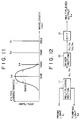
- Fig. 12 is a block diagram for describing a conventional example.
- the symbols, ⁇ 1 , ⁇ 2 , ⁇ 3 , ... not only denote wavelengths but also signals of those wavelengths.
- Fig. 12 shows a multiplexing section 11 for multiplexing two input signals ⁇ 1 , ⁇ 2 and outputting their multiplexed waves ⁇ 1 , ⁇ 2 .
- a mixer section 12 uses a device such as an optical semiconductor amplifier or a differential frequency generator using a KTP crystal.
- the mixer section 12 receives inputs of multiplexing signals ⁇ 1 , ⁇ 2 , mixes them, and outputs signals of wavelengths ⁇ 1 , ⁇ 2 , and ⁇ 3 , ⁇ 4 as shown in Figs. 3(a) and 3(b).
- a band-pass filter (B. P.F.) 13 as shown in Figs. 3(a) and 3(b) has a passage band wavelength of ⁇ 4 .
- a probe light of a wavelength ⁇ 1 , and a pumping light of a wavelength ⁇ 2 are inputted to the multiplexing section 11.
- the pumping light is for increasing the nonlinear optical effect.
- the probe light is a reference light.
- the multiplexing section 11 multiplexes the two input signals and outputs a multiplexed wave signal to the mixer section 12.
- the mixer section 12 When the multiplexed wave signal is inputted to the mixer section 12, the mixer section 12, as shown in Fig. 5(a), with nonlinear optical effect, outputs multiplexed wave signals of wavelengths ⁇ 3 , ⁇ 4 distant by ⁇ from the input signals ⁇ 1 , ⁇ 2 .
- the mixer section 12 As shown in Fig. 5(a), with nonlinear optical effect, outputs multiplexed wave signals of wavelengths ⁇ 3 , ⁇ 4 distant by ⁇ from the input signals ⁇ 1 , ⁇ 2 .
- the band-pass filter 13 has its passage band wavelength at ⁇ 4 which is distant by a differential wavelength ⁇ from the pumping light wavelength ⁇ 2 on the opposite side of the probe light wavelength ⁇ 1 .
- the probe light signal of the wavelength ⁇ 1 is converted to the output light signal of the wavelength ⁇ 4 .
- ⁇ 3 or ⁇ 4 may be used as the mixer output, since the wavelength is not so distant from that of the input signal, even if it is filtered with a band-pass filter of the passage band ⁇ 4 as shown in Fig. 3(b), the signals ⁇ 1 , ⁇ 2 are not easy to cut off.
- the gain characteristic peak of the optical semiconductor amplifier is in the vicinity of the two input wavelengths ⁇ 1 , ⁇ 2 and the gain is very low in the vicinity of the output signal wavelength ⁇ 4 . Therefore, conversion efficiency (output signal to input signal) is very low (10 -4 or less).
- a wavelength-converted output signal comes out as a spatial light beam either in the form of a sum frequency wave, differential frequency wave, or second harmonic wave.
- Figs. 4(a)-4(d) show relationship between the input wavelength and output wavelength (frequency).
- Fig. 4(b) shows the case in which the frequency of the output signal is the sum of the frequencies of the two input signals at wavelengths ⁇ 1 , ⁇ 2 .
- Fig. 4(c) shows the case in which the frequency of the output signal is the difference between the frequencies of the two input signals at wavelengths ⁇ 1 , ⁇ 2 .
- Fig. 4(d) shows the case in which the wavelengths of the output signals are respectively half the two input signal wavelengths by cutting off the input waves.
- the process using the spatial light beam requires a certain size and makes installation less easy. Furthermore, with the differential frequency generation, like the optical semiconductor amplifier, since the wavelengths of input and output signals are not largely different from each other, it is less easy to cut off the input signal with a filter.
- a pumping light of the wavelength ⁇ 2 is used to produce an output signal which is apart by the differential wavelength ⁇ , and the output signal is measured.
- a disadvantage in that case is that, when the two input wavelengths ⁇ 1 , ⁇ 2 are close to the wavelength ⁇ 4 , the input wave component contained in the output cannot be completely cut off and the property of the probe light cannot be known accurately.
- the present invention has been made with the foregoing problems of the conventional device in view.
- an optical parametric diffuser comprising:
- Fig. 1 is a block diagram showing a constitution of an embodiment of the invention.
- a multiplexing section 1 is for multiplexing two input signals ⁇ 1 , ⁇ 2 and outputting their multiplexed wave signals ⁇ 1 , ⁇ 2 .
- a mixer section 2 receives inputs of multiplexing signals ⁇ 1 , ⁇ 2 from the multiplexing section 1, mixes them, amplifies them, and outputs signals of wavelengths ⁇ 1 , ⁇ 2 , and ⁇ 3 , ⁇ 4 , ⁇ 5 as shown in Fig. 6.
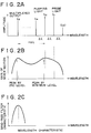
- a band-pass filter 3 has its pass band at the wavelength ⁇ 5 as shown in Fig. 2(c).
- the probe light of the wavelength ⁇ 1 and the pumping light of the wavelength ⁇ 2 are inputted to the multiplexing section 1.
- the pumping light is for starting up the nonlinear optical effect and the probe light (also called as reference light) is for converting its wavelength from now on.
- the multiplexing section 1 multiplexes the two input signals and outputs the multiplexed signals to the mixer section 2.
- the gain of the mixer section has its peak in the vicinity of the wavelengths ⁇ 1 , ⁇ 2 and the gain is small in the vicinity of the wavelengths ⁇ 5 , ⁇ 6 . Therefore, the multiplexed wave components of the wavelengths ⁇ 5 , ⁇ 6 are buried below the noise level, and cannot be taken out as output signals. In the embodiment of the invention, however, since the peak is shifted toward the wavelength ⁇ 5 as shown in Fig. 6(b), the wavelength ⁇ 5 can be taken out as a multiplexed wave signal.
- the efficiency of the mixer is extremely enhanced to produce very large output signals.
- the band-pass filter 3 as shown in Fig. 11 has its pass band at the wavelength ⁇ 5 which is apart from the probe light wavelength ⁇ 1 by n ⁇ (which is n times the wavelength difference ⁇ between the two input signals) on the opposite side of the pumping light wavelength ⁇ 2 .
- the probe light signal of the wavelength ⁇ 1 is converted to the output signal of the wavelength ⁇ 5 .
- a laser diode having either of the following two characteristics may be used as the mixer section 2.
- the active region of the laser diode of the Application is constituted with a light containment layer, a plural number of quantum well layers, and barrier layers placed among the quantum well layers and in contact with them. At least one of the plural number of quantum well layers is different in thickness from the others and with lattice non-alignment. And an embodiment is disclosed which amplifies wavelength from 1.45 - 1.54 ⁇ m in the 1.5 ⁇ m band by adjusting the layer thickness and amount of distortion of the plural number of quantum well layers.
- the laser diode having the second peak is made with the second output signal generation efficiency peak at ⁇ 5 by adjusting the layer thickness to agree with the wavelength at the time of manufacture.
- the laser diode having a plural number of layers is made of a wide band type by adjusting each layer thickness so that one wavelength has its signal generation efficiency peak at a low level and the other at the second level.
- the reflection factor of the end surface mirrors is made less than 1/1000 and carrier is injected.
- OPD amplifies the signal and oscillates.
- the reflectivity of the end surface mirrors 21 shown in Fig. 8 is kept as low as 1/1000 - 1/100,000 to raise the amplification-oscillation threshold so that OPD oscillates when the energy reaches the second level at an intended layer as shown in Fig. 9.
- the quantum well laser diode uses two types of alternately laminated composition materials for the active layer.
- Fig. 8 uses a quantum well laser diode 20 as the mixer section 2 shown in Fig. 1.
- the quantum well laser diode 20 as shown in Fig. 8 is provided with end surface mirrors 21a, 21b on both ends between which is disposed an active layer consisting of two types of composition materials stacked alternately in heterojunction quantum well structure 22.
- the symbol 23 denotes a carrier injection power source.
- Fig. 10 shows the energy band of the quantum well laser diode 20.
- the quantum well laser diode in which very thin films of two different materials are alternately laminated, electrons are stable at a low energy level. As a result, electrons may be locally distributed in the potential well layer where the energy of the conduction band bottom is low.
- the potential barrier layer becomes a barrier because of its high energy of the conduction band bottom. Since only the number of waves which become a standing wave are allowed to the electrons bound to the potential well layer, the wavelength is determined with the layer thickness. Therefore, the layer thickness should be adjusted to obtain the light of the intended wavelength.
- the quantum well laser diode 20 With the quantum well laser diode 20, electrons are stable at a low energy level. When energy is gradually injected, the energy collects in the potential well layer as shown in Fig. 10, and generally when the layer is saturated, oscillation begins. Since the reflection factor of the end surface mirrors 21a, 21b is kept as low as about 1/10,000, this quantum well laser diode does not oscillate here but oscillates when the energy reaches the next level.
- the potential well layer in multiple layers with some layers in different thicknesses and different energy levels so as to cause oscillation in a plural number of wavelengths.
- the state density of the above arrangement as shown in Fig. 9 occurs in stepped values.
- Carrier is injected to accumulate energy to the second level and oscillate.
- energy value is four times that of the minimum level, the wavelength may be set more widely apart than that of wavelength adjustment with a normal layer thickness.
- the energy band structure of the quantum well laser is as shown in Fig. 10 and oscillation tends to occur with energy gap between the lowest of the conduction band of the potential well layer and the highest of the valence electron band.
- electrons cannot exist in the potential well layer at the lowest energy of the conduction band, and can only exist when a standing wave occurs in the potential well layer.
- the energy level when the number of waves in the standing wave is minimum is called the minimum level.
- the energy level that electrons can take becomes n 2 times the minimum level.
- the energy level that the hole can take is only that when the standing wave is generated, and the value is n 2 times the minimum level.
- the thickness of the potential well layer and the potential barrier layer is 1 micrometers
- the energy gap of the potential barrier layer is 0.24 eV on the valence electron band side and 1.35 eV on the conduction band side
- the wavelength due to the energy gap Eg between the minimum energy in the potential well layer of the conduction band and the maximum energy in the valence band is 1600 nm.
- the energy at the minimum level corresponds to the wavelength 30 nm on the conduction band side and 5 nm on the valence band side. Therefore, oscillation wavelengths at the minimum and the second levels are respectively,
- wavelength setting is made possible in a wider range than with the conventional layer thickness adjustment at the minimum level, even when the probe light wavelength ⁇ 1 , the pumping light wavelength ⁇ 2 , and the output signal of the wavelength ⁇ 5 are apart from each other.
- the output spectrum of the mixer section 2 using the quantum well type of laser diode is shown in Fig. 2(a) and Fig. 11.
- the signal generation efficiency when the multiple layer quantum well type of laser diode described above is used as the mixer 2 is shown in Fig. 2(b). As shown, it is possible to set the peak resulting from the two input wavelengths ⁇ 1 , ⁇ 2 with a slight shift toward ⁇ 5 to produce a peak resulting from the second level at the wavelength ⁇ 5 .
- This optical parametric diffuser may be used for example in optical sampling observation of the output wavelength ⁇ 5 converted from the probe light wavelength ⁇ 1 with the pumping light in pulses.
- the above embodiment is described in the case in which the pumping light wavelength ⁇ 2 is shorter than the probe light wavelength ⁇ 1 and the output wavelength ⁇ 5 is shorter than the pumping light wavelength ⁇ 2 .
- this invention may also be applied to the case in which the pumping light wavelength ⁇ 2 is longer than the probe light wavelength ⁇ 1 and the output wavelength ⁇ 5 is longer than the pumping light wavelength ⁇ 2 by interchanging the peak of the gain of the mixer section resulting from the minimum level and the peak of the gain of the mixer section resulting from the second level.
- This invention makes it possible to cut off an input signal easily by utilizing an output wavelength ⁇ 5 which is apart from the input signal by n ⁇ (n is any integer not less than 2).
- the apparatus is made more compact than that using a KTP crystal and with an extremely high conversion efficiency (10 -2 or more).
Landscapes
- Physics & Mathematics (AREA)
- Nonlinear Science (AREA)
- General Physics & Mathematics (AREA)
- Optics & Photonics (AREA)
- Condensed Matter Physics & Semiconductors (AREA)
- Electromagnetism (AREA)
- Optical Modulation, Optical Deflection, Nonlinear Optics, Optical Demodulation, Optical Logic Elements (AREA)
- Optical Communication System (AREA)
Applications Claiming Priority (3)
| Application Number | Priority Date | Filing Date | Title |
|---|---|---|---|
| JP16268796 | 1996-06-24 | ||
| JP162687/96 | 1996-06-24 | ||
| JP16268796 | 1996-06-24 |
Publications (2)
| Publication Number | Publication Date |
|---|---|
| EP0817339A1 true EP0817339A1 (de) | 1998-01-07 |
| EP0817339B1 EP0817339B1 (de) | 2000-10-18 |
Family
ID=15759397
Family Applications (1)
| Application Number | Title | Priority Date | Filing Date |
|---|---|---|---|
| EP97301565A Expired - Lifetime EP0817339B1 (de) | 1996-06-24 | 1997-03-10 | Optischer Wellenlängenkonverter |
Country Status (3)
| Country | Link |
|---|---|
| US (1) | US5940206A (de) |
| EP (1) | EP0817339B1 (de) |
| DE (1) | DE69703317T2 (de) |
Families Citing this family (1)
| Publication number | Priority date | Publication date | Assignee | Title |
|---|---|---|---|---|
| US6744553B1 (en) * | 2000-06-20 | 2004-06-01 | Xtera Communications, Inc. | System and method for converting a plurality of wavelengths |
Citations (2)
| Publication number | Priority date | Publication date | Assignee | Title |
|---|---|---|---|---|
| EP0426239A1 (de) * | 1989-10-31 | 1991-05-08 | Koninklijke Philips Electronics N.V. | Optischer Verstärker |
| JPH06283824A (ja) * | 1993-03-25 | 1994-10-07 | Anritsu Corp | 光増幅素子 |
Family Cites Families (3)
| Publication number | Priority date | Publication date | Assignee | Title |
|---|---|---|---|---|
| US3675039A (en) * | 1971-02-09 | 1972-07-04 | Bell Telephone Labor Inc | Coherent optical devices employing zinc germanium phosphide |
| US4528464A (en) * | 1983-02-28 | 1985-07-09 | At&T Bell Laboratories | Degenerate four-wave mixer using multiple quantum well structures |
| JPH0792513A (ja) * | 1993-09-22 | 1995-04-07 | Oki Electric Ind Co Ltd | 波長変換素子及びその使用方法 |
-
1997
- 1997-03-07 US US08/813,907 patent/US5940206A/en not_active Expired - Fee Related
- 1997-03-10 DE DE69703317T patent/DE69703317T2/de not_active Expired - Fee Related
- 1997-03-10 EP EP97301565A patent/EP0817339B1/de not_active Expired - Lifetime
Patent Citations (2)
| Publication number | Priority date | Publication date | Assignee | Title |
|---|---|---|---|---|
| EP0426239A1 (de) * | 1989-10-31 | 1991-05-08 | Koninklijke Philips Electronics N.V. | Optischer Verstärker |
| JPH06283824A (ja) * | 1993-03-25 | 1994-10-07 | Anritsu Corp | 光増幅素子 |
Non-Patent Citations (3)
| Title |
|---|
| BAVA G P ET AL: "FREQUENCY CONVERSION IN TRAVELLING WAVE SEMICONDUCTOR LASER AMPLIFIERS WITH BULK AND QUANTUM WELL STRUCTURES", IEE PROCEEDINGS: OPTOELECTRONICS, vol. 143, no. 2, pages 119 - 125, XP000593990 * |
| D'OTTAVI A ET AL: "FOUR-WAVE MIXING IN A STRAINED MULTIPLE-QUANTUM-WELL AMPLIFIER", PROCEEDINGS OF THE QUANTUM ELECTRONICS AND LASER SCIENCE CONFERENCE, BALTIMORE, MAY 2 - 7, 1993, vol. 12, INSTITUTE OF ELECTRICAL AND ELECTRONICS ENGINEERS, pages 189/190, XP000398231 * |
| PATENT ABSTRACTS OF JAPAN vol. 95, no. 1 28 February 1995 (1995-02-28) * |
Also Published As
| Publication number | Publication date |
|---|---|
| US5940206A (en) | 1999-08-17 |
| DE69703317D1 (de) | 2000-11-23 |
| EP0817339B1 (de) | 2000-10-18 |
| DE69703317T2 (de) | 2001-03-15 |
Similar Documents
| Publication | Publication Date | Title |
|---|---|---|
| US4253060A (en) | RF Spectrum analyzer | |
| US7830527B2 (en) | Multiple frequency optical mixer and demultiplexer and apparatus for remote sensing | |
| US3660673A (en) | Optical parametric device | |
| US6738397B2 (en) | Solid-state light source apparatus | |
| DE69307013T2 (de) | Integriertes, nichtlineares Wellenleiterspektrometer | |
| EP2642659B1 (de) | Abstimmbarer optoelektronischer Oszillator mit schwachem Phasenrauschen | |
| CN113055098B (zh) | 一种光通信波段的频域复用宣布式单光子源 | |
| GB2343964A (en) | A non linear optical device with a varied refractive index | |
| US7026594B2 (en) | Method and device for producing radio frequency waves | |
| EP0817339B1 (de) | Optischer Wellenlängenkonverter | |
| US6795232B2 (en) | Wavelength converter | |
| JP4485745B2 (ja) | 光機能素子および光機能装置 | |
| Koch et al. | Mode locked and distributed feedback silicon evanescent lasers | |
| JP3383800B2 (ja) | 超高速光ミキサ装置 | |
| US6956652B2 (en) | Optical autocorrelator | |
| Previde Massara et al. | Four-wave mixing in a silicon microring resonator using a self-pumping geometry | |
| EP4055671B1 (de) | Modengekoppelter laser mit gräben und zugehörige optische komponente | |
| EP3807960A1 (de) | Verriegelung eines lasers auf einem resonator mittels eines optischen verstärkers | |
| Primiani | Hybrid Integrated opto-electronic oscillators | |
| JP3533199B2 (ja) | 波長変換装置 | |
| EP0727689B1 (de) | Akusto-optisches Wellenleiterbauelement | |
| JP2790536B2 (ja) | 超短光パルス発生装置 | |
| Guzun et al. | Second-harmonic generation with femtosecond pulses and its applications in sub-shot-noise detection | |
| JPH0442590A (ja) | 半導体レーザの高周波応答特性測定装置 | |
| JPH0311116B2 (de) |
Legal Events
| Date | Code | Title | Description |
|---|---|---|---|
| PUAI | Public reference made under article 153(3) epc to a published international application that has entered the european phase |
Free format text: ORIGINAL CODE: 0009012 |
|
| AK | Designated contracting states |
Kind code of ref document: A1 Designated state(s): DE FR GB |
|
| 17P | Request for examination filed |
Effective date: 19980519 |
|
| RAP1 | Party data changed (applicant data changed or rights of an application transferred) |
Owner name: TERATEC CORPORATION |
|
| GRAG | Despatch of communication of intention to grant |
Free format text: ORIGINAL CODE: EPIDOS AGRA |
|
| 17Q | First examination report despatched |
Effective date: 19991217 |
|
| GRAG | Despatch of communication of intention to grant |
Free format text: ORIGINAL CODE: EPIDOS AGRA |
|
| GRAH | Despatch of communication of intention to grant a patent |
Free format text: ORIGINAL CODE: EPIDOS IGRA |
|
| RIC1 | Information provided on ipc code assigned before grant |
Free format text: 7H 01S 5/40 A, 7G 02F 1/35 B |
|
| GRAH | Despatch of communication of intention to grant a patent |
Free format text: ORIGINAL CODE: EPIDOS IGRA |
|
| GRAA | (expected) grant |
Free format text: ORIGINAL CODE: 0009210 |
|
| AK | Designated contracting states |
Kind code of ref document: B1 Designated state(s): DE FR GB |
|
| REF | Corresponds to: |
Ref document number: 69703317 Country of ref document: DE Date of ref document: 20001123 |
|
| ET | Fr: translation filed | ||
| PLBE | No opposition filed within time limit |
Free format text: ORIGINAL CODE: 0009261 |
|
| STAA | Information on the status of an ep patent application or granted ep patent |
Free format text: STATUS: NO OPPOSITION FILED WITHIN TIME LIMIT |
|
| 26N | No opposition filed | ||
| REG | Reference to a national code |
Ref country code: GB Ref legal event code: IF02 |
|
| REG | Reference to a national code |
Ref country code: GB Ref legal event code: 732E |
|
| REG | Reference to a national code |
Ref country code: FR Ref legal event code: TP |
|
| PGFP | Annual fee paid to national office [announced via postgrant information from national office to epo] |
Ref country code: FR Payment date: 20040309 Year of fee payment: 8 |
|
| PGFP | Annual fee paid to national office [announced via postgrant information from national office to epo] |
Ref country code: GB Payment date: 20040310 Year of fee payment: 8 |
|
| PGFP | Annual fee paid to national office [announced via postgrant information from national office to epo] |
Ref country code: DE Payment date: 20040318 Year of fee payment: 8 |
|
| PG25 | Lapsed in a contracting state [announced via postgrant information from national office to epo] |
Ref country code: GB Free format text: LAPSE BECAUSE OF NON-PAYMENT OF DUE FEES Effective date: 20050310 |
|
| PG25 | Lapsed in a contracting state [announced via postgrant information from national office to epo] |
Ref country code: DE Free format text: LAPSE BECAUSE OF NON-PAYMENT OF DUE FEES Effective date: 20051001 |
|
| GBPC | Gb: european patent ceased through non-payment of renewal fee |
Effective date: 20050310 |
|
| PG25 | Lapsed in a contracting state [announced via postgrant information from national office to epo] |
Ref country code: FR Free format text: LAPSE BECAUSE OF NON-PAYMENT OF DUE FEES Effective date: 20051130 |
|
| REG | Reference to a national code |
Ref country code: FR Ref legal event code: ST Effective date: 20051130 |