EP0426239A1 - Optischer Verstärker - Google Patents
Optischer Verstärker Download PDFInfo
- Publication number
- EP0426239A1 EP0426239A1 EP90202835A EP90202835A EP0426239A1 EP 0426239 A1 EP0426239 A1 EP 0426239A1 EP 90202835 A EP90202835 A EP 90202835A EP 90202835 A EP90202835 A EP 90202835A EP 0426239 A1 EP0426239 A1 EP 0426239A1
- Authority
- EP
- European Patent Office
- Prior art keywords
- layers
- layer
- optical amplifier
- active layer
- optical
- Prior art date
- Legal status (The legal status is an assumption and is not a legal conclusion. Google has not performed a legal analysis and makes no representation as to the accuracy of the status listed.)
- Ceased
Links
- 230000003287 optical effect Effects 0.000 title claims abstract description 52
- 230000003321 amplification Effects 0.000 claims abstract description 30
- 238000003199 nucleic acid amplification method Methods 0.000 claims abstract description 30
- 239000000463 material Substances 0.000 claims abstract description 28
- 230000005855 radiation Effects 0.000 claims abstract description 20
- 230000004888 barrier function Effects 0.000 claims abstract description 16
- 230000007704 transition Effects 0.000 claims abstract description 15
- 239000004065 semiconductor Substances 0.000 claims abstract description 14
- PNEYBMLMFCGWSK-UHFFFAOYSA-N Alumina Chemical compound [O-2].[O-2].[O-2].[Al+3].[Al+3] PNEYBMLMFCGWSK-UHFFFAOYSA-N 0.000 claims abstract description 9
- 239000000758 substrate Substances 0.000 claims abstract description 8
- GWEVSGVZZGPLCZ-UHFFFAOYSA-N Titan oxide Chemical compound O=[Ti]=O GWEVSGVZZGPLCZ-UHFFFAOYSA-N 0.000 claims abstract description 7
- GPXJNWSHGFTCBW-UHFFFAOYSA-N Indium phosphide Chemical compound [In]#P GPXJNWSHGFTCBW-UHFFFAOYSA-N 0.000 claims description 9
- IJGRMHOSHXDMSA-UHFFFAOYSA-N Atomic nitrogen Chemical compound N#N IJGRMHOSHXDMSA-UHFFFAOYSA-N 0.000 claims description 6
- 229910052757 nitrogen Inorganic materials 0.000 claims description 6
- XUIMIQQOPSSXEZ-UHFFFAOYSA-N Silicon Chemical compound [Si] XUIMIQQOPSSXEZ-UHFFFAOYSA-N 0.000 claims description 4
- 229910052710 silicon Inorganic materials 0.000 claims description 4
- 239000010703 silicon Substances 0.000 claims description 4
- QVGXLLKOCUKJST-UHFFFAOYSA-N atomic oxygen Chemical compound [O] QVGXLLKOCUKJST-UHFFFAOYSA-N 0.000 claims description 3
- 239000004020 conductor Substances 0.000 claims description 3
- 230000005670 electromagnetic radiation Effects 0.000 claims description 3
- 229910052760 oxygen Inorganic materials 0.000 claims description 3
- 239000001301 oxygen Substances 0.000 claims description 3
- 239000004408 titanium dioxide Substances 0.000 claims description 2
- 238000005253 cladding Methods 0.000 abstract 1
- OGIDPMRJRNCKJF-UHFFFAOYSA-N titanium oxide Inorganic materials [Ti]=O OGIDPMRJRNCKJF-UHFFFAOYSA-N 0.000 abstract 1
- 238000004891 communication Methods 0.000 description 3
- 238000005516 engineering process Methods 0.000 description 3
- 238000000034 method Methods 0.000 description 3
- 239000000203 mixture Substances 0.000 description 3
- 238000010521 absorption reaction Methods 0.000 description 2
- 230000002238 attenuated effect Effects 0.000 description 2
- 238000010586 diagram Methods 0.000 description 2
- 230000000694 effects Effects 0.000 description 2
- 238000002347 injection Methods 0.000 description 2
- 239000007924 injection Substances 0.000 description 2
- TWNQGVIAIRXVLR-UHFFFAOYSA-N oxo(oxoalumanyloxy)alumane Chemical compound O=[Al]O[Al]=O TWNQGVIAIRXVLR-UHFFFAOYSA-N 0.000 description 2
- 238000000103 photoluminescence spectrum Methods 0.000 description 2
- 230000008929 regeneration Effects 0.000 description 2
- 238000011069 regeneration method Methods 0.000 description 2
- 239000000243 solution Substances 0.000 description 2
- 229910020286 SiOxNy Inorganic materials 0.000 description 1
- VYPSYNLAJGMNEJ-UHFFFAOYSA-N Silicium dioxide Chemical compound O=[Si]=O VYPSYNLAJGMNEJ-UHFFFAOYSA-N 0.000 description 1
- 230000006978 adaptation Effects 0.000 description 1
- 230000000903 blocking effect Effects 0.000 description 1
- 239000011248 coating agent Substances 0.000 description 1
- 238000000576 coating method Methods 0.000 description 1
- 239000000470 constituent Substances 0.000 description 1
- 239000004148 curcumin Substances 0.000 description 1
- 239000007789 gas Substances 0.000 description 1
- 238000007689 inspection Methods 0.000 description 1
- 239000007788 liquid Substances 0.000 description 1
- 238000004519 manufacturing process Methods 0.000 description 1
- 229910052751 metal Inorganic materials 0.000 description 1
- 239000002184 metal Substances 0.000 description 1
- 239000013307 optical fiber Substances 0.000 description 1
- 229910052814 silicon oxide Inorganic materials 0.000 description 1
Images

Classifications
-
- B—PERFORMING OPERATIONS; TRANSPORTING
- B82—NANOTECHNOLOGY
- B82Y—SPECIFIC USES OR APPLICATIONS OF NANOSTRUCTURES; MEASUREMENT OR ANALYSIS OF NANOSTRUCTURES; MANUFACTURE OR TREATMENT OF NANOSTRUCTURES
- B82Y20/00—Nanooptics, e.g. quantum optics or photonic crystals
-
- H—ELECTRICITY
- H01—ELECTRIC ELEMENTS
- H01S—DEVICES USING THE PROCESS OF LIGHT AMPLIFICATION BY STIMULATED EMISSION OF RADIATION [LASER] TO AMPLIFY OR GENERATE LIGHT; DEVICES USING STIMULATED EMISSION OF ELECTROMAGNETIC RADIATION IN WAVE RANGES OTHER THAN OPTICAL
- H01S5/00—Semiconductor lasers
- H01S5/02—Structural details or components not essential to laser action
- H01S5/028—Coatings ; Treatment of the laser facets, e.g. etching, passivation layers or reflecting layers
-
- H—ELECTRICITY
- H01—ELECTRIC ELEMENTS
- H01S—DEVICES USING THE PROCESS OF LIGHT AMPLIFICATION BY STIMULATED EMISSION OF RADIATION [LASER] TO AMPLIFY OR GENERATE LIGHT; DEVICES USING STIMULATED EMISSION OF ELECTROMAGNETIC RADIATION IN WAVE RANGES OTHER THAN OPTICAL
- H01S5/00—Semiconductor lasers
- H01S5/20—Structure or shape of the semiconductor body to guide the optical wave ; Confining structures perpendicular to the optical axis, e.g. index or gain guiding, stripe geometry, broad area lasers, gain tailoring, transverse or lateral reflectors, special cladding structures, MQW barrier reflection layers
- H01S5/22—Structure or shape of the semiconductor body to guide the optical wave ; Confining structures perpendicular to the optical axis, e.g. index or gain guiding, stripe geometry, broad area lasers, gain tailoring, transverse or lateral reflectors, special cladding structures, MQW barrier reflection layers having a ridge or stripe structure
- H01S5/227—Buried mesa structure ; Striped active layer
-
- H—ELECTRICITY
- H01—ELECTRIC ELEMENTS
- H01S—DEVICES USING THE PROCESS OF LIGHT AMPLIFICATION BY STIMULATED EMISSION OF RADIATION [LASER] TO AMPLIFY OR GENERATE LIGHT; DEVICES USING STIMULATED EMISSION OF ELECTROMAGNETIC RADIATION IN WAVE RANGES OTHER THAN OPTICAL
- H01S5/00—Semiconductor lasers
- H01S5/30—Structure or shape of the active region; Materials used for the active region
- H01S5/34—Structure or shape of the active region; Materials used for the active region comprising quantum well or superlattice structures, e.g. single quantum well [SQW] lasers, multiple quantum well [MQW] lasers or graded index separate confinement heterostructure [GRINSCH] lasers
- H01S5/343—Structure or shape of the active region; Materials used for the active region comprising quantum well or superlattice structures, e.g. single quantum well [SQW] lasers, multiple quantum well [MQW] lasers or graded index separate confinement heterostructure [GRINSCH] lasers in AIIIBV compounds, e.g. AlGaAs-laser, InP-based laser
- H01S5/3434—Structure or shape of the active region; Materials used for the active region comprising quantum well or superlattice structures, e.g. single quantum well [SQW] lasers, multiple quantum well [MQW] lasers or graded index separate confinement heterostructure [GRINSCH] lasers in AIIIBV compounds, e.g. AlGaAs-laser, InP-based laser with a well layer comprising at least both As and P as V-compounds
-
- H—ELECTRICITY
- H01—ELECTRIC ELEMENTS
- H01S—DEVICES USING THE PROCESS OF LIGHT AMPLIFICATION BY STIMULATED EMISSION OF RADIATION [LASER] TO AMPLIFY OR GENERATE LIGHT; DEVICES USING STIMULATED EMISSION OF ELECTROMAGNETIC RADIATION IN WAVE RANGES OTHER THAN OPTICAL
- H01S5/00—Semiconductor lasers
- H01S5/50—Amplifier structures not provided for in groups H01S5/02 - H01S5/30
-
- H—ELECTRICITY
- H01—ELECTRIC ELEMENTS
- H01S—DEVICES USING THE PROCESS OF LIGHT AMPLIFICATION BY STIMULATED EMISSION OF RADIATION [LASER] TO AMPLIFY OR GENERATE LIGHT; DEVICES USING STIMULATED EMISSION OF ELECTROMAGNETIC RADIATION IN WAVE RANGES OTHER THAN OPTICAL
- H01S5/00—Semiconductor lasers
- H01S5/20—Structure or shape of the semiconductor body to guide the optical wave ; Confining structures perpendicular to the optical axis, e.g. index or gain guiding, stripe geometry, broad area lasers, gain tailoring, transverse or lateral reflectors, special cladding structures, MQW barrier reflection layers
- H01S5/22—Structure or shape of the semiconductor body to guide the optical wave ; Confining structures perpendicular to the optical axis, e.g. index or gain guiding, stripe geometry, broad area lasers, gain tailoring, transverse or lateral reflectors, special cladding structures, MQW barrier reflection layers having a ridge or stripe structure
- H01S5/227—Buried mesa structure ; Striped active layer
- H01S5/2275—Buried mesa structure ; Striped active layer mesa created by etching
- H01S5/2277—Buried mesa structure ; Striped active layer mesa created by etching double channel planar buried heterostructure [DCPBH] laser
-
- H—ELECTRICITY
- H01—ELECTRIC ELEMENTS
- H01S—DEVICES USING THE PROCESS OF LIGHT AMPLIFICATION BY STIMULATED EMISSION OF RADIATION [LASER] TO AMPLIFY OR GENERATE LIGHT; DEVICES USING STIMULATED EMISSION OF ELECTROMAGNETIC RADIATION IN WAVE RANGES OTHER THAN OPTICAL
- H01S5/00—Semiconductor lasers
- H01S5/30—Structure or shape of the active region; Materials used for the active region
- H01S5/34—Structure or shape of the active region; Materials used for the active region comprising quantum well or superlattice structures, e.g. single quantum well [SQW] lasers, multiple quantum well [MQW] lasers or graded index separate confinement heterostructure [GRINSCH] lasers
- H01S5/3418—Structure or shape of the active region; Materials used for the active region comprising quantum well or superlattice structures, e.g. single quantum well [SQW] lasers, multiple quantum well [MQW] lasers or graded index separate confinement heterostructure [GRINSCH] lasers using transitions from higher quantum levels
-
- H—ELECTRICITY
- H01—ELECTRIC ELEMENTS
- H01S—DEVICES USING THE PROCESS OF LIGHT AMPLIFICATION BY STIMULATED EMISSION OF RADIATION [LASER] TO AMPLIFY OR GENERATE LIGHT; DEVICES USING STIMULATED EMISSION OF ELECTROMAGNETIC RADIATION IN WAVE RANGES OTHER THAN OPTICAL
- H01S5/00—Semiconductor lasers
- H01S5/30—Structure or shape of the active region; Materials used for the active region
- H01S5/34—Structure or shape of the active region; Materials used for the active region comprising quantum well or superlattice structures, e.g. single quantum well [SQW] lasers, multiple quantum well [MQW] lasers or graded index separate confinement heterostructure [GRINSCH] lasers
- H01S5/343—Structure or shape of the active region; Materials used for the active region comprising quantum well or superlattice structures, e.g. single quantum well [SQW] lasers, multiple quantum well [MQW] lasers or graded index separate confinement heterostructure [GRINSCH] lasers in AIIIBV compounds, e.g. AlGaAs-laser, InP-based laser
- H01S5/34306—Structure or shape of the active region; Materials used for the active region comprising quantum well or superlattice structures, e.g. single quantum well [SQW] lasers, multiple quantum well [MQW] lasers or graded index separate confinement heterostructure [GRINSCH] lasers in AIIIBV compounds, e.g. AlGaAs-laser, InP-based laser emitting light at a wavelength longer than 1000nm, e.g. InP based 1300 and 1500nm lasers
Definitions
- the invention relates to an optical amplifier with a semiconductor body comprising a substrate of a first conductivity type and a covering layer structure of at least a first passive layer of the first conductivity type, a second passive layer of the second, opposite conductivity type, and between the first and the second passive layer an active layer and a PN junction, in which amplification of electromagnetic radiation occurs within a strip-shaped amplification region of the active layer at a sufficiently high current strength in the forward direction through the PN junction, in which the active layer for the radiation to be amplified has a greater effective refractive index and a smaller effective band gap than the first and the second passive layer, and in which the active layer consists of a number of quantum well layers (referred to as QW layers for simplicity's sake) of a semiconductor material with a direct energy gap, which layers are separated from one another by barrier layers of another semiconductor material, while the strip-shaped amplification region is bounded by end surfaces which are practically perpendicular to the active layer and serve as input and output surfaces for the radiation to be ampl
- Such a semiconductor device is known from the Japanese Patent Application JP-A-56/164588 (publication date 17-12-1981) laid open to public inspection and published in Patent Abstract of Japan, vol. 6, 7 April 1982, no. 52 (E-100), page 23.
- Optical radiation amplifiers are widely used in the quickly developing optical communication technology. Wide distances must often be covered and/or strongly ramified networks must be used in optical telecommunication systems. A weak or attenuated optical signal must then often be regenerated by an optical amplifier once or several times underway.
- Radiation amplification takes place in the active layer in such an amplifier realized by semiconductor technology.
- This amplification is at its maximum at a wavelength which is determined by the choice of semiconductor material of the active layer and by the Fabry-Pérot (FP) resonances, which in their turn are determined by the positions of the end surfaces. If these end surfaces are made non-reflecting or practically non-reflecting by means of an anti-reflection layer, an optical amplifier of the travelling wave type is obtained with a relatively wide-band amplification profile which is determined exclusively by the material amplification.
- the bandwidth of the known optical travelling wave amplifiers described above is in the order of 60 nm. So a bandwidth of 60 nm is insufficient for systems in which both wavelength windows mentioned must be used, which is the case, for example, in the application of multiplex techniques such as in "Local Area Networks", in which information is transmitted via both wavelength windows through the same optical fibre. This means that separate optical amplifiers are required for the regeneration of attenuated signals in this case.
- the present invention has for its object inter alia to provide an optical travelling wave amplifier in which radiation amplification for both wavelength windows can take place in one and the same element.
- the invention is based on the recognition that this can be achieved by means of a suitably chosen structure of the active layer built up of quantum wells.
- an optical amplifier of the type described in the opening paragraph is characterized in that the material, the number and the thickness of the quantum well layers and the barrier layers in combination with the length of the strip-shaped amplification region are so chosen that two optical transitions between the conduction band and the valency band can take place in the active layer, maximum amplification taking place at a certain current density through the PN junction for the radiation wavelengths corresponding to these optical transitions, and in that the end surfaces are provided with an anti-reflection layer which has a reflection coefficient of at most 0,5% for these two wavelengths.
- the two radiation wavelengths having maximum amplification lie preferably between 1280 nm and 1320 nm, and between 1500 nm and 1570 nm.
- the QW layers may be used for various suitable materials. Good results are obtained when the QW layers consist of indium-gallium-arsenic phosphide (InGaAsP) and the barrier layers of indium phosphide (InP).
- InGaAsP indium-gallium-arsenic phosphide
- InP indium phosphide
- Six QW layers, each with a thickness of approximately 9 nm, are advantageously used for this in combination with barrier layers having a thickness of approximately 20 nm.
- the end surfaces must be coated with an anti-reflection layer resulting in a reflection coefficient of at most 0,5% for both wavelengths.
- the application of an anti-reflection layer meeting this specification is not always simple.
- the envisaged effect can be achieved with an anti-reflection layer consisting of N layers, alternately a first layer of a first material and a first, higher refractive index n1, and a second layer of a second material having a second, lower refractive index n2, the optical thickness of each layer being substantially equal to 1/4 the average wavelength of the radiation to be amplified, and the relation between the number N, the refractive index n1 of the first layers and the reactive index n2 of the second layers being given by the equation: in which the value n1xn2 is substantially equal to the effective reactive index of the waveguide structure of the amplifier.
- the first layer of anti-reflection layers applied on III-V junctions advantageously consist of titanium dioxide (TiO2), and the second layers of aluminium oxide (Al2O3) in order to obtain minimum reflection in the said wavelength ranges.
- an accurate mutual adaptation of the various refractive indices may be obtained when at least one of the two materials of the anti-reflection layer consists of silicon oxynitride (SiO x N y ). This is because the reactive index of this material can be varied within certain limits by adjustment of the ratio between oxygen and nitrogen.
- Fig. 1 shows diagrammatically, partly in perspective and partly in cross-section
- Fig. 2 shows diagrammatically in cross-section taken on the line II-II of Fig. 1 an optical amplifier according to the invention.
- the device has a semiconductor body comprising a substrate 1 of a first, in this case the N-conductivity type, and a covering layer structure.
- This layer structure comprises an N-type buffer layer 1A, a first passive layer 2 of the said first, so in this case N-conductivity type, a second passive layer 3 of the second, opposite conductivity type, so in this case the P-type, and between the first passive layer 2 and the second passive layer 3 an active layer 4, in this case of the N-type.
- the said layer structure further comprises a PN junction 6 between the passive layers 2 and 3.
- this PN junction 6 adjoins the P-type layer 3.
- the materials and dimensions of the layers of the said layer structure are chosen in such a way that amplification of electromagnetic radiation (I) takes place within a strip-shaped amplification region of the active layer 4 for certain wavelengths at a sufficiently high current strength (i) in the forward direction through the PN junction.
- the active layer 4 for the radiation I to be amplified here has a greater effective refractive index and a smaller band gap than the first (2) and second (3) passive layers, while the active layer 4 comprises a number of quantum well (QW) layers 4A of a semiconductor material with direct band transition, which layers are separated from one another by barrier layers 4B of a different semiconductor material.
- QW quantum well
- the strip-shaped amplification region whose width is diagrammatically indicated with a in Fig. 1, is bounded by end surfaces 7 and 8 which are pratically perpendicular to the active layer and serve as input and output surfaces for the radiation I to be amplified.
- the second passive layer 3 and the substrate 1 are electrically connected to connection conductors in the form of metal layers 16 and 17, through which a current i can be supplied in the forward direction to the PN junction 6.
- the material, the number, and the thickness of the QW layers 4A and the barrier layers 4B in combination with the length 1 (see Fig. 2) of the strip-shaped amplification region are chosen in such a way that two optical electron transitions can take place in the active layer 4 between the conduction band and the valency band, maximum amplification occurring at a certain current density through the PN junction 6 for the radiation wavelengths corresponding to these optical transitions, while the end surfaces 7 and 8 (see Fig. 2) are each provided with an anti-reflection layer 9 which has a reflection coefficient of at most 0,5% for these two wavelengths.
- the active layer 4 (shown in more detail in Fig. 3) comprises 6 QW layers 4A of N-type indium-gallium-arsenic phosphide in the composition In 0,58 Ga 0,42 As 0,90 P 0,10 and with a thickness of approximately 9 nm. If used as a single active laser layer, this material has an emission wavelength of 1,55 ⁇ m.
- the QW layers 4A are separated from one another by barrier layers of N-type indium phosphide with a thickness of approximately 20 nm.
- An active layer composed in this way leads to an energy diagram as represented in Fig. 2.
- Two different optical electron transitions i.e. between the levels E 2e and E 1hh and between the levels E 1e and E 1hh , can take place with radiation wavelengths of approximately 1300 nm and approximately 1500 nm, respectively, in a quantum well enclosed by two InP layers.
- the relative positions of the two levels E 2e and E 1e can be adjusted within certain limits by variation of the thickness of the QW layers.
- the number of QW layers in combination with the length l of the active strip-shaped region determines the relative amplification of the wavelengths corresponding to the two optical transitions, the saturation effects occurring for the E 1e -E 1hh transition for certain injection current densities being utilized.
- anti-reflection layers must be used which are also effective for both wavelengths. This will be further discussed later.
- the optical amplifier of this example has the well-known DCPBH ("Double Channel Planar Barrier Heter”) structure which is frequently used for optical communication
- DCPBH Double Channel Planar Barrier Heter
- the invention is by no means limited to this structure.
- the DCPBH structure of the optical amplifier comprises a substrate 1 of N-type indium phosphide (doping concentration, for example, 5 x 1018 cm ⁇ 3) with a thickness of, for example, 350 ⁇ m.
- the QW and barrier layers 4A, B and on top of that a buffer layer 5 of N-type indium-gallium-arsenic phosphide with the composition In 0,73 Ga 0,27 As 0,59 P 0,41 , a doping concentration of 1015 and a thickness of
- the device further comprises a current-limiting layer structure.
- This structure comprises two grooves 14 and 15 which delimit the strip-shaped amplification region and in which a layer 11 of P-type indium phosphide with a thickness (outside the grooves) of approximately 0,3 ⁇ m and a doping concentration of 2 x 1018 cm ⁇ 3 and a blocking layer 12 of N-type indium phosphide with a doping concentration of approximately 1018 cm ⁇ 3 and a thickness of approximately 0,5 ⁇ m are provided.
- the layers 11 and 12 do not extend over the strip-shaped portion of the layer 5 present between the grooves 14 and 15, so that the P-type second passive layer 3 in the mesa-shaped amplification region between the grooves 14 and 15 (width of mesa 1,7 ⁇ m) directly adjoins the N-type buffer layer 5.
- a silicon oxide layer 10 in which a longitudinal opening is formed, within which an electrode layer 16 applied on the upper surface makes contact with the layer 13.
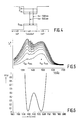
- Fig. 5 shows the photoluminescence spectrum for the optical amplifier according to this embodiment.
- the photoluminescent intensity (arbitrary units) at 300 K as a function of the wavelength in nm is shown for various values of the injection current i .
- an optical amplifier according to the invention can function correctly only if an anti-reflection layer is applied both on the input surface and on the output surface, which layer reduces to an acceptable minimum the reflection of both wavelengths to be amplified.
- an anti-reflection layer consisting of N layers, alternately a first layer of a first material and a first, higher refractive index n1, and a second layer of a second material having a second, lower reactive index n2, the optical thickness of each layer being substantially equal to 1/4 the average wavelength of the radiation to be amplified, and the relation between the number N, the refractive index n1 of the first layers and the refractive index n2 of the second layers being given by the equation: in which the value n1xn2 is substantially equal to the effective refractive index of the waveguide structure of the amplifier.
- the reflection coefficient R can be kept below 0,5% over a wide wavelength range.
- the refractive index values 2,08 and 1,56 correspond substantially to those of titanium dioxide (TiO2) and aluminium oxide (Al2O3), respectively, a good result can be obtained with an anti-reflection layer 9 consisting of four layers, i.e. alternately a layer of TiO2 and a layer of Al2O3, each layer having an optical thickness of approximately 1/4 wavelength, see Fig. 2.
- Fig. 6 shows the reflection coefficient as a function of wavelength for such an anti-reflection layer. Multiple reflections have been included in the calculations for this Figure. It can be seen that the reflection coefficient in this case shows minima exactly near the desired wavelengths. This renders this anti-reflection coating eminently suitable for use in the optical amplifier according to the invention.
- a very suitable material for at least one of the constituent layers of the anti-reflection layer can be formed by silicon oxynitride.
- the reactive index can be varied between approximately 1,44 and approximately 2,05 in that case by adjustment of the oxygen/nitrogen ratio, so that a very good control of the desired reflection coefficient is possible.
- anti-reflection layer structure is obviously not limited to optical amplifiers, but may also be of advantage in all those cases where an anti-reflection layer with a wide effective window is required.
- the invention is not limited to the embodiment described herein, but can be used in other amplifier structures than those of the DCPBH type. Moreover, other dimensions, materials, and layer thicknesses may be used, if so desired, depending on the values of the two wavelengths used, without departing from the scope of the invention.
Landscapes
- Physics & Mathematics (AREA)
- Optics & Photonics (AREA)
- Condensed Matter Physics & Semiconductors (AREA)
- General Physics & Mathematics (AREA)
- Electromagnetism (AREA)
- Engineering & Computer Science (AREA)
- Nanotechnology (AREA)
- Chemical & Material Sciences (AREA)
- Biophysics (AREA)
- Crystallography & Structural Chemistry (AREA)
- Life Sciences & Earth Sciences (AREA)
- Geometry (AREA)
- Semiconductor Lasers (AREA)
- Optical Integrated Circuits (AREA)
- Photo Coupler, Interrupter, Optical-To-Optical Conversion Devices (AREA)
Applications Claiming Priority (2)
| Application Number | Priority Date | Filing Date | Title |
|---|---|---|---|
| NL8902685 | 1989-10-31 | ||
| NL8902685 | 1989-10-31 |
Publications (1)
| Publication Number | Publication Date |
|---|---|
| EP0426239A1 true EP0426239A1 (de) | 1991-05-08 |
Family
ID=19855538
Family Applications (1)
| Application Number | Title | Priority Date | Filing Date |
|---|---|---|---|
| EP90202835A Ceased EP0426239A1 (de) | 1989-10-31 | 1990-10-24 | Optischer Verstärker |
Country Status (3)
| Country | Link |
|---|---|
| US (1) | US5196958A (de) |
| EP (1) | EP0426239A1 (de) |
| JP (1) | JPH03168620A (de) |
Cited By (7)
| Publication number | Priority date | Publication date | Assignee | Title |
|---|---|---|---|---|
| EP0562173A1 (de) * | 1992-02-27 | 1993-09-29 | Mitsubishi Denki Kabushiki Kaisha | Optische Halbleitervorrichtung |
| WO1995002910A1 (en) * | 1993-07-12 | 1995-01-26 | British Telecommunications Public Limited Company | Electrical barrier structure for semiconductor device |
| WO1996019023A3 (en) * | 1994-12-12 | 1996-08-15 | Philips Electronics Nv | Semiconductor diode laser amplifier and method of manufacturing same |
| EP0817339A1 (de) * | 1996-06-24 | 1998-01-07 | Teratek Corporation | Optischer Wellenlängekonverter |
| EP1317034A3 (de) * | 2001-11-01 | 2005-04-06 | The Furukawa Electric Co., Ltd. | Halbleiterlaser mit Beschichtung mit niedrigem Reflektionsvermögen |
| EP0991153A4 (de) * | 1998-01-26 | 2006-01-11 | Furukawa Electric Co Ltd | Halbleiterlasermodul |
| US7858427B2 (en) | 2009-03-03 | 2010-12-28 | Applied Materials, Inc. | Crystalline silicon solar cells on low purity substrate |
Families Citing this family (14)
| Publication number | Priority date | Publication date | Assignee | Title |
|---|---|---|---|---|
| JP2677006B2 (ja) * | 1990-10-24 | 1997-11-17 | 松下電器産業株式会社 | 光増幅器および光伝送装置 |
| EP0562518B1 (de) * | 1992-03-23 | 1997-12-29 | Canon Kabushiki Kaisha | Optische Vorrichtung und Methode unter Benutzung dieser Vorrichtung, welche die Änderung einer über die beiden Anschlussenden eines verstärkenden Bereichs abfallenden Spannung ausnutzt |
| JP2555955B2 (ja) * | 1993-11-11 | 1996-11-20 | 日本電気株式会社 | 半導体光増幅器およびその製造方法 |
| US6307668B1 (en) | 1999-10-04 | 2001-10-23 | Optigain, Inc. | Ultra-wide bandwidth fiber based optical amplifier |
| SG102589A1 (en) * | 2000-08-16 | 2004-03-26 | Inst Materials Research & Eng | Buried hetero-structure opto-electronic device |
| US6750156B2 (en) | 2001-10-24 | 2004-06-15 | Applied Materials, Inc. | Method and apparatus for forming an anti-reflective coating on a substrate |
| KR100853241B1 (ko) * | 2005-12-16 | 2008-08-20 | 샤프 가부시키가이샤 | 질화물 반도체 발광소자 및 질화물 반도체 레이저 소자의제조방법 |
| JP5191650B2 (ja) * | 2005-12-16 | 2013-05-08 | シャープ株式会社 | 窒化物半導体発光素子および窒化物半導体発光素子の製造方法 |
| JP5004597B2 (ja) * | 2006-03-06 | 2012-08-22 | シャープ株式会社 | 窒化物半導体発光素子および窒化物半導体発光素子の製造方法 |
| JP5430826B2 (ja) | 2006-03-08 | 2014-03-05 | シャープ株式会社 | 窒化物半導体レーザ素子 |
| JP4444304B2 (ja) * | 2006-04-24 | 2010-03-31 | シャープ株式会社 | 窒化物半導体発光素子および窒化物半導体発光素子の製造方法 |
| KR101656510B1 (ko) * | 2014-10-29 | 2016-09-30 | 주식회사 스마트씨솔루션 | 기저귀 용변 감지 시스템 |
| WO2016187568A1 (en) | 2015-05-21 | 2016-11-24 | Wave Sensor, Inc. | Monitoring incontinence events |
| CN116569345A (zh) * | 2020-11-27 | 2023-08-08 | 苏州晶湛半导体有限公司 | GaN基激光器及其制作方法 |
Citations (4)
| Publication number | Priority date | Publication date | Assignee | Title |
|---|---|---|---|---|
| US4589115A (en) * | 1983-09-09 | 1986-05-13 | Xerox Corporation | Wavelength tuning of quantum well heterostructure lasers using an external grating |
| EP0254568A2 (de) * | 1986-07-25 | 1988-01-27 | Mitsubishi Denki Kabushiki Kaisha | Halbleiterlaservorrichtung |
| EP0321087A1 (de) * | 1987-12-14 | 1989-06-21 | BRITISH TELECOMMUNICATIONS public limited company | Antireflektions-Schichten |
| EP0103415B1 (de) * | 1982-08-12 | 1989-10-04 | Fujitsu Limited | Lichtemittierende Vorrichtungen und Verfahren zu deren Herstellung |
Family Cites Families (6)
| Publication number | Priority date | Publication date | Assignee | Title |
|---|---|---|---|---|
| US3868589A (en) * | 1972-10-10 | 1975-02-25 | Univ California | Thin film devices and lasers |
| US4439782A (en) * | 1980-11-21 | 1984-03-27 | University Of Illinois Foundation | Semiconductor device with heterojunction of Alx Ga1-x As--AlAs--Ga |
| US4525687A (en) * | 1983-02-28 | 1985-06-25 | At&T Bell Laboratories | High speed light modulator using multiple quantum well structures |
| US4616241A (en) * | 1983-03-22 | 1986-10-07 | The United States Of America As Represented By The United States Department Of Energy | Superlattice optical device |
| US4727555A (en) * | 1983-09-02 | 1988-02-23 | Xerox Corporation | Wavelength tuned quantum well lasers |
| US4875216A (en) * | 1987-11-30 | 1989-10-17 | Xerox Corporation | Buried waveguide window regions for improved performance semiconductor lasers and other opto-electronic applications |
-
1990
- 1990-10-23 US US07/603,977 patent/US5196958A/en not_active Expired - Fee Related
- 1990-10-24 EP EP90202835A patent/EP0426239A1/de not_active Ceased
- 1990-10-29 JP JP2288617A patent/JPH03168620A/ja active Pending
Patent Citations (4)
| Publication number | Priority date | Publication date | Assignee | Title |
|---|---|---|---|---|
| EP0103415B1 (de) * | 1982-08-12 | 1989-10-04 | Fujitsu Limited | Lichtemittierende Vorrichtungen und Verfahren zu deren Herstellung |
| US4589115A (en) * | 1983-09-09 | 1986-05-13 | Xerox Corporation | Wavelength tuning of quantum well heterostructure lasers using an external grating |
| EP0254568A2 (de) * | 1986-07-25 | 1988-01-27 | Mitsubishi Denki Kabushiki Kaisha | Halbleiterlaservorrichtung |
| EP0321087A1 (de) * | 1987-12-14 | 1989-06-21 | BRITISH TELECOMMUNICATIONS public limited company | Antireflektions-Schichten |
Non-Patent Citations (3)
| Title |
|---|
| IEEE JOURNAL OF QUANTUM ELECTRONICS, vol. 24, no. 11, November 1988, pages 2178-2190, IEEE, New York, US; K. MAGARI et al.: "Optical narrow-band filters using optical amplification with distributed feedback" * |
| PATENT ABSTRACTS OF JAPAN, vol. 6, no. 195 (P-146), 5th October 1982; & JP-A-57 104 902 (SEIKO EPSON CORP.) 30-06-1982 * |
| TECHNICAL DIGEST OF THE EUROPEAN CONFERENCE ON OPTICAL COMMUNICATION 1987, part III, POST DEADLINE PAPERS, Helsinki, 13th - 17th September 1987, pages 13-16; P.J.A. THIJS et al.: "DCPBH-laser diodes with an MOVPE grown separate confinement (SC)-multiple quantum well (MQW) active region, emitting at 2 = 1.5 mum" * |
Cited By (10)
| Publication number | Priority date | Publication date | Assignee | Title |
|---|---|---|---|---|
| EP0562173A1 (de) * | 1992-02-27 | 1993-09-29 | Mitsubishi Denki Kabushiki Kaisha | Optische Halbleitervorrichtung |
| WO1995002910A1 (en) * | 1993-07-12 | 1995-01-26 | British Telecommunications Public Limited Company | Electrical barrier structure for semiconductor device |
| EP0639875A1 (de) * | 1993-07-12 | 1995-02-22 | BRITISH TELECOMMUNICATIONS public limited company | Elektrische Sperrstruktur für Halbleiter-Vorrichtung |
| US5838025A (en) * | 1993-07-12 | 1998-11-17 | British Telecommunications Public Limited Company | Electrical barrier structure for semiconductor device doped with chromium and/or titanium |
| WO1996019023A3 (en) * | 1994-12-12 | 1996-08-15 | Philips Electronics Nv | Semiconductor diode laser amplifier and method of manufacturing same |
| EP0817339A1 (de) * | 1996-06-24 | 1998-01-07 | Teratek Corporation | Optischer Wellenlängekonverter |
| US5940206A (en) * | 1996-06-24 | 1999-08-17 | Teratec Corporation | Optical parametric diffuser |
| EP0991153A4 (de) * | 1998-01-26 | 2006-01-11 | Furukawa Electric Co Ltd | Halbleiterlasermodul |
| EP1317034A3 (de) * | 2001-11-01 | 2005-04-06 | The Furukawa Electric Co., Ltd. | Halbleiterlaser mit Beschichtung mit niedrigem Reflektionsvermögen |
| US7858427B2 (en) | 2009-03-03 | 2010-12-28 | Applied Materials, Inc. | Crystalline silicon solar cells on low purity substrate |
Also Published As
| Publication number | Publication date |
|---|---|
| JPH03168620A (ja) | 1991-07-22 |
| US5196958A (en) | 1993-03-23 |
Similar Documents
| Publication | Publication Date | Title |
|---|---|---|
| EP0426239A1 (de) | Optischer Verstärker | |
| CA2048203C (en) | Optical amplifier | |
| EP0469793A2 (de) | Monolithisch integrierter optischer Verstärker und Photodetektor | |
| EP0431527A2 (de) | Optisches Kopplergerät mit wellenlängeselektivem optischem Koppler | |
| US5103455A (en) | Monolithically integrated semiconductor optical preamplifier | |
| JPH05507175A (ja) | 光・電気装置 | |
| GB2080609A (en) | Tapered stripe semiconductor laser | |
| GB2131610A (en) | Semiconductor laser | |
| JP2724827B2 (ja) | 赤外発光素子 | |
| US5260959A (en) | Narrow beam divergence laser diode | |
| US5054871A (en) | Semiconductor waveguide and impedance-matched detector | |
| JPH10200209A (ja) | 半導体光増幅素子 | |
| US4899361A (en) | Optical filter device | |
| US6186631B1 (en) | Two-section semiconductor optical amplifier | |
| JPH05226789A (ja) | 歪層量子井戸レーザを含む製品 | |
| US5666455A (en) | Waveguide device | |
| JP3306892B2 (ja) | 半導体光集積素子およびその製造方法 | |
| US5299057A (en) | Monolithically integrated optical amplifier and photodetector tap | |
| US4745616A (en) | Semiconductor laser device with a diffraction grating | |
| US4758535A (en) | Method for producing semiconductor laser | |
| JP2924834B2 (ja) | 光半導体素子及びその製造方法 | |
| EP0269061A2 (de) | Optische Filtervorrichtung | |
| JPH10223921A (ja) | 半導体受光素子とその製造方法 | |
| JP2869875B2 (ja) | 光集積回路の製造方法 | |
| JP3025322B2 (ja) | 光導波路 |
Legal Events
| Date | Code | Title | Description |
|---|---|---|---|
| PUAI | Public reference made under article 153(3) epc to a published international application that has entered the european phase |
Free format text: ORIGINAL CODE: 0009012 |
|
| AK | Designated contracting states |
Kind code of ref document: A1 Designated state(s): DE FR GB IT NL SE |
|
| 17P | Request for examination filed |
Effective date: 19911104 |
|
| 17Q | First examination report despatched |
Effective date: 19930428 |
|
| APAB | Appeal dossier modified |
Free format text: ORIGINAL CODE: EPIDOS NOAPE |
|
| STAA | Information on the status of an ep patent application or granted ep patent |
Free format text: STATUS: THE APPLICATION HAS BEEN REFUSED |
|
| 18R | Application refused |
Effective date: 19980402 |
|
| APAF | Appeal reference modified |
Free format text: ORIGINAL CODE: EPIDOSCREFNE |