EP0818782A2 - Verfahren zur Bereitstellung von Grafik auf plastischen Informationsplatten - Google Patents
Verfahren zur Bereitstellung von Grafik auf plastischen Informationsplatten Download PDFInfo
- Publication number
- EP0818782A2 EP0818782A2 EP97304898A EP97304898A EP0818782A2 EP 0818782 A2 EP0818782 A2 EP 0818782A2 EP 97304898 A EP97304898 A EP 97304898A EP 97304898 A EP97304898 A EP 97304898A EP 0818782 A2 EP0818782 A2 EP 0818782A2
- Authority
- EP
- European Patent Office
- Prior art keywords
- layer
- method defined
- substrate
- metal
- disc
- Prior art date
- Legal status (The legal status is an assumption and is not a legal conclusion. Google has not performed a legal analysis and makes no representation as to the accuracy of the status listed.)
- Granted
Links
- 238000000034 method Methods 0.000 title claims description 29
- 229920002120 photoresistant polymer Polymers 0.000 claims abstract description 54
- 239000000758 substrate Substances 0.000 claims abstract description 47
- 239000000463 material Substances 0.000 claims abstract description 21
- 229910052751 metal Inorganic materials 0.000 claims description 28
- 239000002184 metal Substances 0.000 claims description 28
- 238000009792 diffusion process Methods 0.000 claims description 8
- 238000007788 roughening Methods 0.000 claims description 4
- 238000005488 sandblasting Methods 0.000 claims description 3
- 238000007747 plating Methods 0.000 claims description 2
- 239000011248 coating agent Substances 0.000 claims 2
- 238000000576 coating method Methods 0.000 claims 2
- 238000000151 deposition Methods 0.000 claims 2
- 238000005530 etching Methods 0.000 claims 1
- 238000011161 development Methods 0.000 abstract description 3
- 238000004049 embossing Methods 0.000 abstract 1
- 239000010410 layer Substances 0.000 description 60
- 229910052782 aluminium Inorganic materials 0.000 description 6
- XAGFODPZIPBFFR-UHFFFAOYSA-N aluminium Chemical compound [Al] XAGFODPZIPBFFR-UHFFFAOYSA-N 0.000 description 6
- 238000000465 moulding Methods 0.000 description 5
- PXHVJJICTQNCMI-UHFFFAOYSA-N Nickel Chemical compound [Ni] PXHVJJICTQNCMI-UHFFFAOYSA-N 0.000 description 4
- 239000011241 protective layer Substances 0.000 description 3
- 239000011347 resin Substances 0.000 description 3
- 229920005989 resin Polymers 0.000 description 3
- KRHYYFGTRYWZRS-UHFFFAOYSA-N Fluorane Chemical compound F KRHYYFGTRYWZRS-UHFFFAOYSA-N 0.000 description 2
- 230000008859 change Effects 0.000 description 2
- 238000003486 chemical etching Methods 0.000 description 2
- 230000000295 complement effect Effects 0.000 description 2
- 239000011521 glass Substances 0.000 description 2
- 239000004922 lacquer Substances 0.000 description 2
- 238000012986 modification Methods 0.000 description 2
- 230000004048 modification Effects 0.000 description 2
- 229910052759 nickel Inorganic materials 0.000 description 2
- 238000007639 printing Methods 0.000 description 2
- 230000008569 process Effects 0.000 description 2
- 238000012545 processing Methods 0.000 description 2
- 238000012216 screening Methods 0.000 description 2
- 239000000126 substance Substances 0.000 description 2
- 230000000007 visual effect Effects 0.000 description 2
- 239000000853 adhesive Substances 0.000 description 1
- 230000001070 adhesive effect Effects 0.000 description 1
- 230000004075 alteration Effects 0.000 description 1
- 230000000694 effects Effects 0.000 description 1
- 238000005516 engineering process Methods 0.000 description 1
- 238000004519 manufacturing process Methods 0.000 description 1
- 230000015654 memory Effects 0.000 description 1
- 229910001507 metal halide Inorganic materials 0.000 description 1
- 150000005309 metal halides Chemical class 0.000 description 1
- 238000001579 optical reflectometry Methods 0.000 description 1
- 230000035807 sensation Effects 0.000 description 1
- 238000012546 transfer Methods 0.000 description 1
Images

Classifications
-
- G—PHYSICS
- G03—PHOTOGRAPHY; CINEMATOGRAPHY; ANALOGOUS TECHNIQUES USING WAVES OTHER THAN OPTICAL WAVES; ELECTROGRAPHY; HOLOGRAPHY
- G03F—PHOTOMECHANICAL PRODUCTION OF TEXTURED OR PATTERNED SURFACES, e.g. FOR PRINTING, FOR PROCESSING OF SEMICONDUCTOR DEVICES; MATERIALS THEREFOR; ORIGINALS THEREFOR; APPARATUS SPECIALLY ADAPTED THEREFOR
- G03F7/00—Photomechanical, e.g. photolithographic, production of textured or patterned surfaces, e.g. printing surfaces; Materials therefor, e.g. comprising photoresists; Apparatus specially adapted therefor
-
- G—PHYSICS
- G11—INFORMATION STORAGE
- G11B—INFORMATION STORAGE BASED ON RELATIVE MOVEMENT BETWEEN RECORD CARRIER AND TRANSDUCER
- G11B23/00—Record carriers not specific to the method of recording or reproducing; Accessories, e.g. containers, specially adapted for co-operation with the recording or reproducing apparatus ; Intermediate mediums; Apparatus or processes specially adapted for their manufacture
- G11B23/38—Visual features other than those contained in record tracks or represented by sprocket holes the visual signals being auxiliary signals
- G11B23/40—Identifying or analogous means applied to or incorporated in the record carrier and not intended for visual display simultaneously with the playing-back of the record carrier, e.g. label, leader, photograph
-
- G—PHYSICS
- G11—INFORMATION STORAGE
- G11B—INFORMATION STORAGE BASED ON RELATIVE MOVEMENT BETWEEN RECORD CARRIER AND TRANSDUCER
- G11B7/00—Recording or reproducing by optical means, e.g. recording using a thermal beam of optical radiation by modifying optical properties or the physical structure, reproducing using an optical beam at lower power by sensing optical properties; Record carriers therefor
- G11B7/24—Record carriers characterised by shape, structure or physical properties, or by the selection of the material
- G11B7/26—Apparatus or processes specially adapted for the manufacture of record carriers
- G11B7/261—Preparing a master, e.g. exposing photoresist, electroforming
-
- B—PERFORMING OPERATIONS; TRANSPORTING
- B29—WORKING OF PLASTICS; WORKING OF SUBSTANCES IN A PLASTIC STATE IN GENERAL
- B29L—INDEXING SCHEME ASSOCIATED WITH SUBCLASS B29C, RELATING TO PARTICULAR ARTICLES
- B29L2017/00—Carriers for sound or information
- B29L2017/001—Carriers of records containing fine grooves or impressions, e.g. disc records for needle playback, cylinder records
- B29L2017/003—Records or discs
-
- B—PERFORMING OPERATIONS; TRANSPORTING
- B29—WORKING OF PLASTICS; WORKING OF SUBSTANCES IN A PLASTIC STATE IN GENERAL
- B29L—INDEXING SCHEME ASSOCIATED WITH SUBCLASS B29C, RELATING TO PARTICULAR ARTICLES
- B29L2031/00—Other particular articles
- B29L2031/722—Decorative or ornamental articles
-
- Y—GENERAL TAGGING OF NEW TECHNOLOGICAL DEVELOPMENTS; GENERAL TAGGING OF CROSS-SECTIONAL TECHNOLOGIES SPANNING OVER SEVERAL SECTIONS OF THE IPC; TECHNICAL SUBJECTS COVERED BY FORMER USPC CROSS-REFERENCE ART COLLECTIONS [XRACs] AND DIGESTS
- Y10—TECHNICAL SUBJECTS COVERED BY FORMER USPC
- Y10T—TECHNICAL SUBJECTS COVERED BY FORMER US CLASSIFICATION
- Y10T428/00—Stock material or miscellaneous articles
- Y10T428/21—Circular sheet or circular blank
Definitions
- This invention relates to plastic information discs such as digital video discs (“DVDs”), compact discs (“CDs”), compact disc read-only memories (“CD ROMs”), and the like, and more particularly to providing visible image information (“artwork”) on such discs.
- DVDs digital video discs
- CDs compact discs
- CD ROMs compact disc read-only memories
- artwork visible image information
- Such pit art may be produced using technology similar to that used to record or store information on the disc, but instead of the features being generally microscopic (and apparently random to the naked eye) for information recording, more macroscopic features are employed to produce a visible image.
- Pit art can provide many interesting visual effects, and because it is produced during molding of the disc, it may reduce or eliminate the need for separate printing steps. However, there may be some complexity associated with translating a desired visual image into pit art form.
- a layer of photoresist material typically disposed on a substrate surface, is exposed to the desired visible image (e.g., by placing a transparency of the visible image over the photoresist layer and shining light on the photoresist layer through the visible image).
- the light from the image photo-chemically changes (“exposes”) the photoresist material to different depths in different regions of the image.
- the photoresist layer is relatively dark or opaque, only a relatively small amount of randomly scattered light reaches the photoresist layer and exposes that layer to random depths which are less than the full thickness of the layer. Where the image is relatively light or transparent, enough light reaches the photoresist layer to expose that layer all the way through to the substrate.
- the photoresist layer is "developed” (e.g., placed in a photoresist developer solution). This removes the exposed photoresist material.
- the resulting patterned surface of the remaining photoresist material and some now-uncovered substrate surface is used to produce a similar pattern in the surface of a forming member to be used in forming discs (in particular, forming one of the two, substantially planar, major surfaces of each disc).
- similar pattern means either the same pattern or a complementary pattern analogous to the relationship between positive and negative forms in molding processes generally.
- the forming member is used in the mold in which discs are molded so that the visible image is molded into the disc surface as part of the disc molding process.
- the forming member surface is randomized (corresponding to dark or opaque areas in the original image)
- the forming member gives the resulting disc a light, frosted appearance due to the random scattering of light impinging on those portions of the disc.
- the forming member surface is smoother (corresponding to light or transparent areas in the original image)
- the forming member gives the resulting disc a dark, polished or mirror-like appearance due to the more regular reflection of light impinging on those portions of the disc.
- the substrate surface may be smooth (as is assumed above) or roughened (e.g., by sand blasting or chemical etching).
- a roughened substrate surface gives the portions of the visible image that are associated with uncovered portions of the substrate surface a brushed appearance (which may contrast with the above-mentioned frosted-appearing portions of the image).
- FIG. 1 is a simplified elevational view of an illustrative disc made in accordance with this invention.
- FIG. 2 is a simplified sectional view taken along the line 2-2 in FIG. 1. For greater clarity, section lines have not been employed in FIG. 2 or any of the subsequent FIGS.
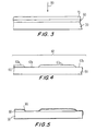
- FIG. 3 is a simplified sectional view of illustrative structure used in accordance with this invention.
- FIG. 4 shows portions of the structure of FIG. 3 at a later stage in their use in accordance with the invention.
- FIG. 5 shows a still later stage of use of the above-mentioned structure in accordance with the invention.
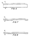
- FIG. 6 shows a further development of the structure of FIG. 5 in accordance with the invention.
- FIG. 7 shows further processing of one of the elements from FIG. 6.
- FIG. 8 shows further processing of one of the elements from FIG. 7.
- DVDs digital video discs
- FIGS. 1 and 2 a DVD 10 is typically made of two CD-type discs 20 and 30 glued back-to-back.
- FIGS. 1 and 2 illustrate the case in which only one of these two discs is needed for information recording.
- the other disc can then be used entirely for artwork in accordance with this invention. If both discs are needed for information recording, then artwork in accordance with this invention can be confined to portions of either disc that are not needed for such information recording.
- lower disc 20 is used for information recording
- upper disc 30 is used for visible image information in accordance with this invention.
- Discs 20 and 30 are held together by a layer of adhesive 40 between the "backs" of the discs.
- Information is recorded on disc 20 in the form of a very long spiral “track", along which a succession of "pits" and "lands” are formed (e.g., molded) in the plastic surface. These pits and lands are indicated by features 22a and 22b in FIG. 2.
- a thin layer 24 of aluminum is applied to this surface to make the pits and lands machine-readable by light reflection through the substantially clear plastic 21 which is the major component of the disc.
- a protective layer 26 of resin such as lacquer is applied over the aluminum.
- Visible image disc 30 may be constructed in a generally similar way.
- the visible image information is formed into a surface of the plastic as represented by features such as 32a and 32b. This surface is covered with a thin layer 34 of aluminum, and the aluminum is covered with a protective layer 36 of resin.
- the image information is visible to a user of the disc by the way light is reflected from aluminum layer 34 through substantially clear plastic 31.
- Element 50 is a substrate member such as a glass plate.
- One surface of substrate 50 is coated with a layer 60 of photoresist material such as Shipley S1818 AZ photoresist having a 15% concentration.
- An illustrative thickness of layer 60 is approximately 1 micron.
- the substrate and photoresist layer are baked (e.g., for about 30 minutes at 80°C) to set the photoresist material.
- Transparency 70 may be a conventional positive film and a diffusion sheet.
- the diffusion sheet is a translucent film with a frosted appearance for helping to ensure that the frosted-appearing image portions described below are produced. Any other suitable image source may be used.
- the next step is to shine light 80 on photoresist layer 60 through image-bearing member 70.
- the source of light 80 may be a 1000 watt metal halide lamp which is operated for about 30 seconds.
- the light reaching layer 60 exposes the photoresist material of that layer to a depth proportional to the amount of light received in each region of the layer.
- image 70 is relatively dark or opaque, only a relatively small amount of randomly scattered light reaches photoresist layer 60 and exposes that layer to random depths which are less than the full thickness of the layer.
- the image 70 is relatively light or transparent, enough light reaches photoresist layer 60 to expose that layer all the way through to substrate 50.
- exposure or the like is used herein to refer to the photo-chemical change which occurs in photoresist material when it receives light. This photo-chemical change renders the exposed material soluble in photoresist developer solution.
- FIG. 4 is a simplified depiction of how substrate 50 and what remains of layer 60 may appear after development as described above. In regions such as 62a some of photoresist layer 60 remains, albeit with a randomly roughened surface due to the relatively small amount of randomly scattered light that reached those portions of layer 60 through associated relatively dark or opaque portions of image 70.
- a photoresist developer solution e.g., a 20% concentration of Shipley microposit developer solution for 25 seconds.
- region 62b on the other hand, all of the photoresist material has been removed to uncover a portion of the surface of substrate 50. Regions 62b are therefore associated with relatively light or transparent portions of image 70 through which sufficient light passed to expose photoresist layer 60 all the way through to substrate 50. For convenience in what follows, regions 62a and 62b are sometimes referred to collectively as surface 62.
- the next steps are performed to transfer the shape of surface 62 to a member that can be used to form disc surfaces. In a particularly preferred embodiment this is done in the same general way that is conventionally used to produce the forming member that is used to record information (pits and lands) in a disc.
- Elements 50 and 60 as shown in FIG. 4, are placed in an atmosphere of metal vapor such as nickel vapor.
- a thin layer 90 of metal deposits or condenses on surface 62 as shown in FIG. 5.
- the structure shown in FIG. 5 is then put in a metal plating solution to plate more metal (e.g., more nickel) on surface 62 as shown in FIG. 6.
- the thicker metal layer shown in FIG. 6 continues to be identified by the reference number 90.
- the lower surface of layer 90 conforms exactly to surface 62. Accordingly, the lower surface of layer 90 is randomly rough in regions corresponding to surface regions 62a, but smooth in regions corresponding to surface regions 62b.
- metal layer 90 which is now sufficiently thick and strong to retain its shape unsupported, is removed from elements 50 and 60.
- Metal layer 90 is used as a "master" to shape complementary metal "intermediaries" 92 as shown in FIG. 7.
- intermediaries 92 may be made from one master 90 by several successive repetitions of steps such as the following: (1) passivate the surface of the master, (2) plate metal on the passivated surface, and (3) separate the newly plated metal from the master to produce the intermediary.
- Several forming members 94 may then be produced from each intermediary 92 by repeating, with the intermediary, steps like those used to make the intermediary from master 90.
- Each forming member 94 (also known as a "stamper”) is usable as an interior surface of a mold in which the plastic portion 31 of discs 30 (FIGS. 1 and 2) are molded. Accordingly, a forming member 94 used in this way imparts its surface shape to the surface 32 of the plastic part of the disc.
- a layer 34 of a light-reflective metal such as aluminum is deposited on patterned plastic surface 32, and then a protective layer 36 of resin such as lacquer is deposited over the metal layer.
- the artwork embossed in surface 32 is rendered highly visible by light reflected through substantially clear plastic 31 by similarly patterned metal layer 34 on surface 32.
- surface regions 32a may correspond to surface regions 62a in FIG. 4. In that case regions 32a are randomly rough (like regions 62a) and scatter light that falls on them. Regions 32a therefore appear light or frosted and produce light areas in the disc artwork.
- Regions 32b may correspond to surface regions 62b in FIG. 4. Regions 32b therefore have the surface features of substrate 50 (assumed in this embodiment to be smooth). Accordingly, regions 32b have more uniform light reflectivity and thus appear mirror-like and dark, thereby producing dark areas in the disc artwork. Indeed, continuing with the assumption that substrate 50 is smooth, regions 32b tend to have a polished appearance, which contrasts strongly with the frosted appearance of regions 32a.
- Another way to produce images of the type described above is to first briefly expose the entire surface of the photoresist layer to light through a diffusion sheet of the type described above. This exposes the photoresist layer all over to relatively shallow random depths (less than the full thickness of the photoresist layer). Then the photoresist layer is further exposed to light through a transparency bearing image information.
- the transparency includes relatively light or transparent regions through which sufficient light can pass to expose the photoresist layer all the way down to the substrate. Elsewhere the transparency does not allow significant alteration of the photoresist layer exposure produced by the diffusion sheet.
- the photoresist layer is then developed and further processed as described above.
- Portions of the resulting disc image that are associated with photoresist layer exposure due primarily to the diffusion sheet have a frosty or light appearance. Portions of the resulting disc image that are associated with photoresist layer exposure all the way down to the substrate have a polished, dark, or mirror-like appearance. Similar results are produced if the sequence of exposures of the photoresist layer is reversed (i.e., if the photoresist layer is first exposed to light through the image bearing transparency and then exposed to light through the diffusion sheet).
- various shades of light and dark can be produced from substantially conventional half-tone original artwork 70.
- the size of the half-tone dots determines the apparent overall lightness or darkness of each image region.
- These dots are effectively preserved in a forming member made in accordance with this invention as roughened regions (corresponding to regions 62a in FIG. 4) in the surface of the forming member.
- the dimensions of these roughened regions, as well as their spacing from adjacent similar features, affect light reflection from the resulting metal layer 34, and thereby impart different sensations of lightness or darkness similar to the tone variations in the original image.
- the surface of substrate 50 on which photoresist layer 60 is deposited is textured (e.g., by sand blasting or by chemical etching such as with hydrofluoric acid if substrate 50 is glass), then portions of the disc image associated with regions 62b (FIG. 4) will have a brushed metal appearance.
- the roughening of that surface is preferably such that the maximum height of substrate surface features under photoresist layer 60 is in the range from about 300 nanometers to about 1000 nanometers.
- Layer 60 is preferably initially thick enough to more than fill in all the surface features on the substrate surface.
- the average initial thickness of layer 60 may be in the range from about 300 nanometers to about 1000 nanometers.
- the light areas of original image 70 allow light 80 to expose layer 60 all the way down to the substrate surface. This causes the roughened substrate surface to be uncovered as at 62b in FIG. 4. This in turn causes a forming member 94 ultimately produced in accordance with the invention to have the roughened texture of the substrate surface. This roughened texture is imparted to corresponding portions of the disc image, giving those portions the above-described brushed metal appearance.
Landscapes
- Physics & Mathematics (AREA)
- General Physics & Mathematics (AREA)
- Engineering & Computer Science (AREA)
- Manufacturing & Machinery (AREA)
- Optical Record Carriers And Manufacture Thereof (AREA)
- Manufacturing Optical Record Carriers (AREA)
- Photosensitive Polymer And Photoresist Processing (AREA)
- Laminated Bodies (AREA)
- Non-Silver Salt Photosensitive Materials And Non-Silver Salt Photography (AREA)
Applications Claiming Priority (4)
| Application Number | Priority Date | Filing Date | Title |
|---|---|---|---|
| US2156096P | 1996-07-11 | 1996-07-11 | |
| US21560P | 1996-07-11 | ||
| US08/714,302 US5958651A (en) | 1996-07-11 | 1996-09-18 | Methods for providing artwork on plastic information discs |
| US714302 | 1996-09-18 |
Publications (3)
| Publication Number | Publication Date |
|---|---|
| EP0818782A2 true EP0818782A2 (de) | 1998-01-14 |
| EP0818782A3 EP0818782A3 (de) | 1998-08-05 |
| EP0818782B1 EP0818782B1 (de) | 2004-04-07 |
Family
ID=26694832
Family Applications (1)
| Application Number | Title | Priority Date | Filing Date |
|---|---|---|---|
| EP97304898A Expired - Lifetime EP0818782B1 (de) | 1996-07-11 | 1997-07-04 | Verfahren zur Bereitstellung von Grafik auf plastischen Informationsplatten |
Country Status (7)
| Country | Link |
|---|---|
| US (1) | US5958651A (de) |
| EP (1) | EP0818782B1 (de) |
| JP (1) | JPH10106052A (de) |
| AT (1) | ATE263999T1 (de) |
| AU (1) | AU725792B2 (de) |
| DE (1) | DE69728474T2 (de) |
| SG (1) | SG50026A1 (de) |
Cited By (7)
| Publication number | Priority date | Publication date | Assignee | Title |
|---|---|---|---|---|
| WO1998041983A1 (en) * | 1997-03-20 | 1998-09-24 | Imation Corp. | Customized graphics for optical discs |
| WO1999004395A1 (en) * | 1997-07-15 | 1999-01-28 | Harmonic Hall Optical Disc Ltd. | Creation of graphic images on a data disc |
| US5946286A (en) * | 1997-03-20 | 1999-08-31 | Imation Corp. | Customized graphics for dual layer optical discs |
| EP0865040A3 (de) * | 1997-03-13 | 2000-01-12 | Wea Manufacturing Inc. | Verfahren zur Bereitstellung von generischen und spezifischen Grafiken auf plastischen Informationsplatten |
| EP0984442A3 (de) * | 1998-09-03 | 2001-03-21 | Wea Manufacturing Inc. | Informationsträger und Verfahren zur Herstellung |
| EP1852860A4 (de) * | 2005-02-18 | 2008-07-02 | Fujifilm Corp | Optisches aufzeichnungsmedium und herstellungsverfahren dafür, substrat und dessen verwendung, matrize und herstellungsverfahren dafür |
| EP2216786A1 (de) * | 2006-05-05 | 2010-08-11 | Moser Baer India Ltd. | Zweilagige optische Platte und Herstellungsverfahren dafür |
Families Citing this family (38)
| Publication number | Priority date | Publication date | Assignee | Title |
|---|---|---|---|---|
| US6423478B1 (en) * | 2000-04-05 | 2002-07-23 | Eastman Kodak Company | Method of forming a watermark image in a hybrid optical master disc |
| US7294294B1 (en) * | 2000-10-17 | 2007-11-13 | Seagate Technology Llc | Surface modified stamper for imprint lithography |
| US7268794B2 (en) * | 2000-10-30 | 2007-09-11 | Yamaha Corporation | Method of printing label on optical disk, optical disk unit, and optical disk |
| JP3956756B2 (ja) * | 2001-10-31 | 2007-08-08 | ヤマハ株式会社 | 光ディスク記録装置 |
| JP4062976B2 (ja) * | 2002-05-31 | 2008-03-19 | ヤマハ株式会社 | 光ディスクへの画像形成装置および画像形成方法 |
| JP3758614B2 (ja) | 2002-06-28 | 2006-03-22 | ヤマハ株式会社 | 光ディスク記録装置及び光ディスクに対する画像形成方法 |
| WO2004012193A1 (ja) * | 2002-07-30 | 2004-02-05 | Matsushita Electric Industrial Co., Ltd. | ディスクカートリッジ |
| US7219840B2 (en) * | 2003-01-17 | 2007-05-22 | Hewlett-Packard Development Company, L.P. | Calibrating fine actuator using a reference pattern |
| US20040141445A1 (en) * | 2003-01-17 | 2004-07-22 | Hanks Darwin Mitchel | Radial position registration for a trackless optical disc surface |
| US7671880B2 (en) * | 2003-01-17 | 2010-03-02 | Hewlett-Packard Development Company, L.P. | Optical disk labeling system and method |
| US7196715B2 (en) * | 2003-01-17 | 2007-03-27 | Hewlett-Packard Development Company, L.P. | Speed control using drive current profile |
| US6862033B2 (en) | 2003-02-14 | 2005-03-01 | Hewlett-Packard Development Company, L.P. | Disc media marking |
| US6866354B2 (en) * | 2003-04-22 | 2005-03-15 | Hewlett-Packard Development Company, L.P. | Disk shape determining and labeling system |
| US20050058044A1 (en) * | 2003-09-12 | 2005-03-17 | Koegler John M. | Optical disk modified for speed and orientation tracking |
| US20050058031A1 (en) * | 2003-09-12 | 2005-03-17 | Hanks Darwin Mitchel | Optical disk drive focusing apparatus |
| US20050058043A1 (en) * | 2003-09-12 | 2005-03-17 | Koegler John M. | Optical disk drive modified for speed and orientation tracking |
| US7177246B2 (en) * | 2003-09-12 | 2007-02-13 | Hewlett-Packard Development Company, L.P. | Optical disk drive focusing apparatus using sum signal |
| US7084894B2 (en) * | 2003-09-12 | 2006-08-01 | Hewlett-Packard Development Company, L.P. | Optical disc drive focusing apparatus |
| US7212688B2 (en) * | 2003-12-30 | 2007-05-01 | A. Zahner Co. | Computer program and method for converting an image to machine control data |
| US20050180306A1 (en) * | 2004-01-29 | 2005-08-18 | Valley Jeffrey M. | Disk labeling kit and method |
| US7496026B2 (en) * | 2004-12-11 | 2009-02-24 | Hewlett-Packard Development Company, L.P. | Optical disc and method of printing optical disc |
| US7324419B2 (en) * | 2004-12-11 | 2008-01-29 | Hewlett-Packard Development Company, L.P. | Focus control via AC input signal |
| US20090015594A1 (en) * | 2005-03-18 | 2009-01-15 | Teruo Baba | Audio signal processing device and computer program for the same |
| US7906194B2 (en) * | 2005-03-31 | 2011-03-15 | Cinram International Inc. | Optical disc with textured edge |
| US7978583B2 (en) * | 2005-05-24 | 2011-07-12 | Cinram International Inc. | Apparatus and method for forming reflective layer of optical disc |
| US20060274617A1 (en) * | 2005-06-03 | 2006-12-07 | Musto James J | Techniques for forming burst cutting area mark |
| US20070090006A1 (en) * | 2005-10-26 | 2007-04-26 | Jeffery Kelsch | Spindle sleeve |
| US7684309B2 (en) | 2005-11-03 | 2010-03-23 | Cinram International Inc. | Multi-purpose high-density optical disc |
| US8675464B2 (en) | 2005-11-03 | 2014-03-18 | Cinram Group, Inc. | Dual sided optical storage media and method for making same |
| US7986611B1 (en) | 2007-03-22 | 2011-07-26 | Cinram International Inc. | High-density optical recording media and method for making same |
| US7910191B1 (en) | 2006-03-09 | 2011-03-22 | Cinram International Inc. | Method for forming light-transmitting cover layer for optical recording medium |
| US20110096655A1 (en) * | 2006-03-09 | 2011-04-28 | Cinram International Inc. | Forming light-transmitting cover layer for recording medium |
| US20080223743A1 (en) * | 2007-03-12 | 2008-09-18 | Gary Lenkeit | Ecofriendly package for CDs and DVDs |
| US7946015B1 (en) | 2007-11-07 | 2011-05-24 | Cinram International Inc. | Method and apparatus for separating dummy disc from multi-layer substrate for optical storage medium |
| US20090127142A1 (en) * | 2007-11-15 | 2009-05-21 | Jeff Rothstein | Optical disc enclosure incorporating fragrance atomizer |
| US8739299B1 (en) | 2009-12-24 | 2014-05-27 | Cinram Group, Inc. | Content unlocking |
| US8369196B1 (en) | 2010-05-04 | 2013-02-05 | Cinram International Inc. | BCA recording on optical recording medium |
| US8526282B1 (en) | 2010-07-07 | 2013-09-03 | Cinram Group, Inc. | Method for replicating media using unique identifiers |
Family Cites Families (30)
| Publication number | Priority date | Publication date | Assignee | Title |
|---|---|---|---|---|
| US3689078A (en) * | 1969-06-30 | 1972-09-05 | Yasujiro Ban | Colored recording discs |
| NL161284C (nl) * | 1972-09-02 | 1980-01-15 | Philips Nv | Weergavestelsel voor een optisch uitleesbare informatie- structuur, alsmede registratiedrager voor gebruik daarin. |
| JPS537201A (en) * | 1976-07-08 | 1978-01-23 | Belge Fab Disques | Method of producing player record |
| US4144300A (en) * | 1976-09-15 | 1979-03-13 | Joseph P. Rolles | Chemical etching of record patterns and the like |
| US4254544A (en) * | 1978-06-21 | 1981-03-10 | Barker Michael D | Method of casting photographic representation having tonal and height contrasts and the article so cast |
| JPS5668903A (en) * | 1979-11-09 | 1981-06-09 | Toppan Printing Co Ltd | Record disk and manufacture of record disk |
| JPS57169938A (en) * | 1981-04-10 | 1982-10-19 | Sony Corp | Optical type recording medium |
| US4629668A (en) * | 1985-03-12 | 1986-12-16 | Quixote Corporation | Optically read recording medium and method for making same |
| JPH0650876Y2 (ja) * | 1987-03-31 | 1994-12-21 | 三洋電機株式会社 | 光学式オーディオディスク |
| EP0374256B1 (de) * | 1988-04-12 | 1998-02-25 | Dai Nippon Insatsu Kabushiki Kaisha | Optisches aufzeichnungsmedium und methode zu dessen herstellung |
| JPH0728590Y2 (ja) * | 1988-09-29 | 1995-06-28 | パイオニア株式会社 | 光学式情報記録担体 |
| US4967286A (en) * | 1988-12-12 | 1990-10-30 | Disctronics Manufacturing, Inc. | Method and apparatus for forming a digital image on an optical recording disc |
| JP2514261B2 (ja) * | 1990-01-11 | 1996-07-10 | 松下電器産業株式会社 | 光情報媒体、その製造方法、及びそのカセットケ―ス |
| JP3109866B2 (ja) * | 1990-11-17 | 2000-11-20 | 太陽誘電株式会社 | 光学式情報記録担体用基板及びその製造方法 |
| CA2066936A1 (en) * | 1991-05-16 | 1992-11-17 | Donald Spector | Compact disc package |
| US5255262A (en) * | 1991-06-04 | 1993-10-19 | International Business Machines Corporation | Multiple data surface optical data storage system with transmissive data surfaces |
| GB9112791D0 (en) * | 1991-06-13 | 1991-07-31 | Applied Holographics | Optical data storage disc |
| JPH0554599A (ja) * | 1991-08-26 | 1993-03-05 | Nec Corp | 光デイスク |
| GB9122247D0 (en) * | 1991-10-19 | 1991-12-04 | Applied Holographics | Optical data storage disc |
| US5470627A (en) * | 1992-03-06 | 1995-11-28 | Quantum Corporation | Double-sided optical media for a disk storage device |
| AU5364094A (en) * | 1992-10-27 | 1994-05-24 | Pmdc, Inc. | Optically readable information disc including visible ornamental hologram, and method of fabricating same |
| TW247960B (de) * | 1992-11-16 | 1995-05-21 | Canon Kk | |
| TW440024U (en) * | 1993-07-28 | 2001-06-07 | Sega Enterprises Kk | Information storage media |
| FR2710443B1 (fr) * | 1993-09-22 | 1995-11-10 | Digipress Sa | Procédé d'enregistrement d'informations sur un disque optique et de lecture de celles-ci, support d'enregistrement et agencement de lecture pour la mise en Óoeuvre du procédé. |
| US5607188A (en) * | 1994-06-24 | 1997-03-04 | Imation Corp. | Marking of optical disc for customized identification |
| FR2725069B1 (fr) * | 1994-09-28 | 1997-01-03 | Digipress Sa | Disque compact comportant un marquage anti-piratage, moule de pressage et procede de marquage anti-piratage de disques compacts |
| EP0706178B1 (de) * | 1994-10-03 | 2001-05-16 | Matsushita Electric Industrial Co., Ltd. | Optisches Informationsmedium, sowie Einheit und Verfahren zu dessen Herstellung |
| JPH08194972A (ja) * | 1995-01-12 | 1996-07-30 | Pioneer Video Corp | 光ディスク及びその製造装置 |
| US5729533A (en) * | 1995-09-12 | 1998-03-17 | Wae Manufacturing Inc. | Two-sided, light-readable information recording disc stacks and methods of making same |
| FR2749432B1 (fr) * | 1996-05-31 | 1998-07-10 | Digipress Sa | Procede de fabrication d'un disque maitre pour la realisation de matrices de pressage de disques optiques comportant un marquage, notamment anti-piratage, disque maitre, matrice de pressage et disque optique obtenu |
-
1996
- 1996-09-18 US US08/714,302 patent/US5958651A/en not_active Expired - Lifetime
-
1997
- 1997-06-30 SG SG1997002316A patent/SG50026A1/en unknown
- 1997-07-04 DE DE69728474T patent/DE69728474T2/de not_active Expired - Lifetime
- 1997-07-04 AT AT97304898T patent/ATE263999T1/de not_active IP Right Cessation
- 1997-07-04 EP EP97304898A patent/EP0818782B1/de not_active Expired - Lifetime
- 1997-07-09 AU AU28561/97A patent/AU725792B2/en not_active Ceased
- 1997-07-11 JP JP9186940A patent/JPH10106052A/ja active Pending
Cited By (7)
| Publication number | Priority date | Publication date | Assignee | Title |
|---|---|---|---|---|
| EP0865040A3 (de) * | 1997-03-13 | 2000-01-12 | Wea Manufacturing Inc. | Verfahren zur Bereitstellung von generischen und spezifischen Grafiken auf plastischen Informationsplatten |
| WO1998041983A1 (en) * | 1997-03-20 | 1998-09-24 | Imation Corp. | Customized graphics for optical discs |
| US5946286A (en) * | 1997-03-20 | 1999-08-31 | Imation Corp. | Customized graphics for dual layer optical discs |
| WO1999004395A1 (en) * | 1997-07-15 | 1999-01-28 | Harmonic Hall Optical Disc Ltd. | Creation of graphic images on a data disc |
| EP0984442A3 (de) * | 1998-09-03 | 2001-03-21 | Wea Manufacturing Inc. | Informationsträger und Verfahren zur Herstellung |
| EP1852860A4 (de) * | 2005-02-18 | 2008-07-02 | Fujifilm Corp | Optisches aufzeichnungsmedium und herstellungsverfahren dafür, substrat und dessen verwendung, matrize und herstellungsverfahren dafür |
| EP2216786A1 (de) * | 2006-05-05 | 2010-08-11 | Moser Baer India Ltd. | Zweilagige optische Platte und Herstellungsverfahren dafür |
Also Published As
| Publication number | Publication date |
|---|---|
| DE69728474T2 (de) | 2004-09-02 |
| ATE263999T1 (de) | 2004-04-15 |
| HK1003281A1 (en) | 1998-10-23 |
| AU725792B2 (en) | 2000-10-19 |
| EP0818782A3 (de) | 1998-08-05 |
| DE69728474D1 (de) | 2004-05-13 |
| US5958651A (en) | 1999-09-28 |
| SG50026A1 (en) | 1998-06-15 |
| AU2856197A (en) | 1998-01-22 |
| JPH10106052A (ja) | 1998-04-24 |
| EP0818782B1 (de) | 2004-04-07 |
Similar Documents
| Publication | Publication Date | Title |
|---|---|---|
| US5958651A (en) | Methods for providing artwork on plastic information discs | |
| AU723223B2 (en) | Methods for providing generic and specific artwork on plastic information discs | |
| US5452282A (en) | Optical data storage disc | |
| EP1143723A3 (de) | Methode zur Herstellung eines Wasserzeichens auf einer hybriden optischen Master Disk | |
| CZ281968B6 (cs) | Opticky snímatelný diskový nosič informace a způsob jeho výroby | |
| CA2221723C (en) | Optical card | |
| HK1003281B (en) | Methods for providing artwork on plastic information discs | |
| JPH08287526A (ja) | 光ディスク原盤製造方法 | |
| JPH02179941A (ja) | 光情報記録媒体及びその製造方法 | |
| US6011767A (en) | Optical data storage disc with a visible holographic image and method for its manufacture | |
| HK1016315B (en) | Method of forming generic and specific visible information on plastic information discs | |
| CN1250540A (zh) | 用于光盘的定制图示 | |
| JP2001014741A (ja) | ディスク原盤及びその製造方法 | |
| JPH08287525A (ja) | 光ディスク原盤製造方法 | |
| EP0810593A1 (de) | Verfahren zur Herstellung einer Originalplatte zur Herstellung von Matrizen für optische Platten mit Markierung, insbesondere Kopierschutzmarkierung, Originalplatte, Matrize, und daraus hergestellte optische Platte | |
| GB2326248A (en) | Optical disc masters | |
| FR2702077A1 (fr) | Procédé de fabrication d'un disque maître et d'une matrice de pressage de disques optiques perfectionnés, disque optique obtenu à partir de ce disque maître ou de cette matrice de pressage. | |
| KR19980084070A (ko) | 광 디스크 제조방법 | |
| JP3724862B2 (ja) | 光カード原版及びその製造方法並びに光カード | |
| WO1999013470A1 (fr) | Disque optique comportant un marquage notamment anti-piratage, et son procede de fabrication | |
| JPH05289302A (ja) | 木材の照りの移動を表現できるエンボス版及びその製造 方法 | |
| JPH0214110A (ja) | カセットの製造法 | |
| JPS63276727A (ja) | 光学的記録媒体の製造方法 | |
| JPS63276726A (ja) | 光学的記録媒体の製造方法 | |
| JPS63181142A (ja) | 光学的記録媒体の製造方法 |
Legal Events
| Date | Code | Title | Description |
|---|---|---|---|
| PUAI | Public reference made under article 153(3) epc to a published international application that has entered the european phase |
Free format text: ORIGINAL CODE: 0009012 |
|
| AK | Designated contracting states |
Kind code of ref document: A2 Designated state(s): AT BE DE FR GB GR IT NL |
|
| PUAL | Search report despatched |
Free format text: ORIGINAL CODE: 0009013 |
|
| AK | Designated contracting states |
Kind code of ref document: A3 Designated state(s): AT BE CH DE DK ES FI FR GB GR IE IT LI LU MC NL PT SE |
|
| 17P | Request for examination filed |
Effective date: 19990114 |
|
| AKX | Designation fees paid |
Free format text: AT BE DE FR GB GR IT NL |
|
| RBV | Designated contracting states (corrected) |
Designated state(s): AT BE DE FR GB GR IT NL |
|
| 17Q | First examination report despatched |
Effective date: 19990707 |
|
| GRAP | Despatch of communication of intention to grant a patent |
Free format text: ORIGINAL CODE: EPIDOSNIGR1 |
|
| GRAS | Grant fee paid |
Free format text: ORIGINAL CODE: EPIDOSNIGR3 |
|
| GRAA | (expected) grant |
Free format text: ORIGINAL CODE: 0009210 |
|
| AK | Designated contracting states |
Kind code of ref document: B1 Designated state(s): AT BE DE FR GB GR IT NL |
|
| REG | Reference to a national code |
Ref country code: GB Ref legal event code: FG4D |
|
| REF | Corresponds to: |
Ref document number: 69728474 Country of ref document: DE Date of ref document: 20040513 Kind code of ref document: P |
|
| PG25 | Lapsed in a contracting state [announced via postgrant information from national office to epo] |
Ref country code: GR Free format text: LAPSE BECAUSE OF FAILURE TO SUBMIT A TRANSLATION OF THE DESCRIPTION OR TO PAY THE FEE WITHIN THE PRESCRIBED TIME-LIMIT Effective date: 20040707 |
|
| REG | Reference to a national code |
Ref country code: HK Ref legal event code: GR Ref document number: 1003281 Country of ref document: HK |
|
| ET | Fr: translation filed | ||
| PLBE | No opposition filed within time limit |
Free format text: ORIGINAL CODE: 0009261 |
|
| STAA | Information on the status of an ep patent application or granted ep patent |
Free format text: STATUS: NO OPPOSITION FILED WITHIN TIME LIMIT |
|
| 26N | No opposition filed |
Effective date: 20050110 |
|
| PGFP | Annual fee paid to national office [announced via postgrant information from national office to epo] |
Ref country code: AT Payment date: 20071121 Year of fee payment: 11 Ref country code: IT Payment date: 20071129 Year of fee payment: 11 |
|
| PGFP | Annual fee paid to national office [announced via postgrant information from national office to epo] |
Ref country code: BE Payment date: 20071213 Year of fee payment: 11 |
|
| PGFP | Annual fee paid to national office [announced via postgrant information from national office to epo] |
Ref country code: GB Payment date: 20071128 Year of fee payment: 11 Ref country code: FR Payment date: 20071119 Year of fee payment: 11 |
|
| GBPC | Gb: european patent ceased through non-payment of renewal fee |
Effective date: 20080704 |
|
| PG25 | Lapsed in a contracting state [announced via postgrant information from national office to epo] |
Ref country code: AT Free format text: LAPSE BECAUSE OF NON-PAYMENT OF DUE FEES Effective date: 20080704 |
|
| REG | Reference to a national code |
Ref country code: FR Ref legal event code: ST Effective date: 20090331 |
|
| PG25 | Lapsed in a contracting state [announced via postgrant information from national office to epo] |
Ref country code: GB Free format text: LAPSE BECAUSE OF NON-PAYMENT OF DUE FEES Effective date: 20080704 |
|
| PG25 | Lapsed in a contracting state [announced via postgrant information from national office to epo] |
Ref country code: IT Free format text: LAPSE BECAUSE OF NON-PAYMENT OF DUE FEES Effective date: 20080704 Ref country code: FR Free format text: LAPSE BECAUSE OF NON-PAYMENT OF DUE FEES Effective date: 20080731 |
|
| PG25 | Lapsed in a contracting state [announced via postgrant information from national office to epo] |
Ref country code: BE Free format text: LAPSE BECAUSE OF NON-PAYMENT OF DUE FEES Effective date: 20080731 |
|
| PGFP | Annual fee paid to national office [announced via postgrant information from national office to epo] |
Ref country code: NL Payment date: 20160711 Year of fee payment: 20 |
|
| PGFP | Annual fee paid to national office [announced via postgrant information from national office to epo] |
Ref country code: DE Payment date: 20160628 Year of fee payment: 20 |
|
| REG | Reference to a national code |
Ref country code: DE Ref legal event code: R071 Ref document number: 69728474 Country of ref document: DE |
|
| REG | Reference to a national code |
Ref country code: NL Ref legal event code: MK Effective date: 20170703 |