EP0820095A2 - Herstellungsverfahren für eine Zwischenschicht - Google Patents
Herstellungsverfahren für eine Zwischenschicht Download PDFInfo
- Publication number
- EP0820095A2 EP0820095A2 EP97111871A EP97111871A EP0820095A2 EP 0820095 A2 EP0820095 A2 EP 0820095A2 EP 97111871 A EP97111871 A EP 97111871A EP 97111871 A EP97111871 A EP 97111871A EP 0820095 A2 EP0820095 A2 EP 0820095A2
- Authority
- EP
- European Patent Office
- Prior art keywords
- film
- interlayer film
- forming
- interlayer
- sio
- Prior art date
- Legal status (The legal status is an assumption and is not a legal conclusion. Google has not performed a legal analysis and makes no representation as to the accuracy of the status listed.)
- Withdrawn
Links
Images


Classifications
-
- H—ELECTRICITY
- H10—SEMICONDUCTOR DEVICES; ELECTRIC SOLID-STATE DEVICES NOT OTHERWISE PROVIDED FOR
- H10P—GENERIC PROCESSES OR APPARATUS FOR THE MANUFACTURE OR TREATMENT OF DEVICES COVERED BY CLASS H10
- H10P14/00—Formation of materials, e.g. in the shape of layers or pillars
- H10P14/60—Formation of materials, e.g. in the shape of layers or pillars of insulating materials
- H10P14/69—Inorganic materials
- H10P14/692—Inorganic materials composed of oxides, glassy oxides or oxide-based glasses
- H10P14/6921—Inorganic materials composed of oxides, glassy oxides or oxide-based glasses containing silicon
- H10P14/69215—Inorganic materials composed of oxides, glassy oxides or oxide-based glasses containing silicon the material being a silicon oxide, e.g. SiO2
-
- H—ELECTRICITY
- H10—SEMICONDUCTOR DEVICES; ELECTRIC SOLID-STATE DEVICES NOT OTHERWISE PROVIDED FOR
- H10P—GENERIC PROCESSES OR APPARATUS FOR THE MANUFACTURE OR TREATMENT OF DEVICES COVERED BY CLASS H10
- H10P14/00—Formation of materials, e.g. in the shape of layers or pillars
- H10P14/60—Formation of materials, e.g. in the shape of layers or pillars of insulating materials
- H10P14/63—Formation of materials, e.g. in the shape of layers or pillars of insulating materials characterised by the formation processes
- H10P14/6326—Deposition processes
- H10P14/6328—Deposition from the gas or vapour phase
- H10P14/6334—Deposition from the gas or vapour phase using decomposition or reaction of gaseous or vapour phase compounds, i.e. chemical vapour deposition
-
- H—ELECTRICITY
- H10—SEMICONDUCTOR DEVICES; ELECTRIC SOLID-STATE DEVICES NOT OTHERWISE PROVIDED FOR
- H10P—GENERIC PROCESSES OR APPARATUS FOR THE MANUFACTURE OR TREATMENT OF DEVICES COVERED BY CLASS H10
- H10P14/00—Formation of materials, e.g. in the shape of layers or pillars
- H10P14/60—Formation of materials, e.g. in the shape of layers or pillars of insulating materials
- H10P14/65—Formation of materials, e.g. in the shape of layers or pillars of insulating materials characterised by treatments performed before or after the formation of the materials
- H10P14/6502—Formation of materials, e.g. in the shape of layers or pillars of insulating materials characterised by treatments performed before or after the formation of the materials of treatments performed before formation of the materials
- H10P14/6506—Formation of intermediate materials
-
- H—ELECTRICITY
- H10—SEMICONDUCTOR DEVICES; ELECTRIC SOLID-STATE DEVICES NOT OTHERWISE PROVIDED FOR
- H10P—GENERIC PROCESSES OR APPARATUS FOR THE MANUFACTURE OR TREATMENT OF DEVICES COVERED BY CLASS H10
- H10P14/00—Formation of materials, e.g. in the shape of layers or pillars
- H10P14/60—Formation of materials, e.g. in the shape of layers or pillars of insulating materials
- H10P14/65—Formation of materials, e.g. in the shape of layers or pillars of insulating materials characterised by treatments performed before or after the formation of the materials
- H10P14/6516—Formation of materials, e.g. in the shape of layers or pillars of insulating materials characterised by treatments performed before or after the formation of the materials of treatments performed after formation of the materials
- H10P14/6529—Formation of materials, e.g. in the shape of layers or pillars of insulating materials characterised by treatments performed before or after the formation of the materials of treatments performed after formation of the materials by exposure to a gas or vapour
- H10P14/6532—Formation of materials, e.g. in the shape of layers or pillars of insulating materials characterised by treatments performed before or after the formation of the materials of treatments performed after formation of the materials by exposure to a gas or vapour by exposure to a plasma
-
- H—ELECTRICITY
- H10—SEMICONDUCTOR DEVICES; ELECTRIC SOLID-STATE DEVICES NOT OTHERWISE PROVIDED FOR
- H10P—GENERIC PROCESSES OR APPARATUS FOR THE MANUFACTURE OR TREATMENT OF DEVICES COVERED BY CLASS H10
- H10P14/00—Formation of materials, e.g. in the shape of layers or pillars
- H10P14/60—Formation of materials, e.g. in the shape of layers or pillars of insulating materials
- H10P14/65—Formation of materials, e.g. in the shape of layers or pillars of insulating materials characterised by treatments performed before or after the formation of the materials
- H10P14/6516—Formation of materials, e.g. in the shape of layers or pillars of insulating materials characterised by treatments performed before or after the formation of the materials of treatments performed after formation of the materials
- H10P14/6534—Formation of materials, e.g. in the shape of layers or pillars of insulating materials characterised by treatments performed before or after the formation of the materials of treatments performed after formation of the materials by exposure to a liquid
-
- H—ELECTRICITY
- H10—SEMICONDUCTOR DEVICES; ELECTRIC SOLID-STATE DEVICES NOT OTHERWISE PROVIDED FOR
- H10P—GENERIC PROCESSES OR APPARATUS FOR THE MANUFACTURE OR TREATMENT OF DEVICES COVERED BY CLASS H10
- H10P14/00—Formation of materials, e.g. in the shape of layers or pillars
- H10P14/60—Formation of materials, e.g. in the shape of layers or pillars of insulating materials
- H10P14/65—Formation of materials, e.g. in the shape of layers or pillars of insulating materials characterised by treatments performed before or after the formation of the materials
- H10P14/6516—Formation of materials, e.g. in the shape of layers or pillars of insulating materials characterised by treatments performed before or after the formation of the materials of treatments performed after formation of the materials
- H10P14/6546—Formation of materials, e.g. in the shape of layers or pillars of insulating materials characterised by treatments performed before or after the formation of the materials of treatments performed after formation of the materials to change the surface groups of the insulating materials
-
- H—ELECTRICITY
- H10—SEMICONDUCTOR DEVICES; ELECTRIC SOLID-STATE DEVICES NOT OTHERWISE PROVIDED FOR
- H10P—GENERIC PROCESSES OR APPARATUS FOR THE MANUFACTURE OR TREATMENT OF DEVICES COVERED BY CLASS H10
- H10P14/00—Formation of materials, e.g. in the shape of layers or pillars
- H10P14/60—Formation of materials, e.g. in the shape of layers or pillars of insulating materials
- H10P14/66—Formation of materials, e.g. in the shape of layers or pillars of insulating materials characterised by the type of materials
- H10P14/662—Laminate layers, e.g. stacks of alternating high-k metal oxides
-
- H—ELECTRICITY
- H10—SEMICONDUCTOR DEVICES; ELECTRIC SOLID-STATE DEVICES NOT OTHERWISE PROVIDED FOR
- H10P—GENERIC PROCESSES OR APPARATUS FOR THE MANUFACTURE OR TREATMENT OF DEVICES COVERED BY CLASS H10
- H10P14/00—Formation of materials, e.g. in the shape of layers or pillars
- H10P14/60—Formation of materials, e.g. in the shape of layers or pillars of insulating materials
- H10P14/66—Formation of materials, e.g. in the shape of layers or pillars of insulating materials characterised by the type of materials
- H10P14/668—Formation of materials, e.g. in the shape of layers or pillars of insulating materials characterised by the type of materials the materials being characterised by the deposition precursor materials
- H10P14/6681—Formation of materials, e.g. in the shape of layers or pillars of insulating materials characterised by the type of materials the materials being characterised by the deposition precursor materials the precursor containing a compound comprising Si
- H10P14/6682—Formation of materials, e.g. in the shape of layers or pillars of insulating materials characterised by the type of materials the materials being characterised by the deposition precursor materials the precursor containing a compound comprising Si the compound being a silane, e.g. disilane, methylsilane or chlorosilane
-
- H—ELECTRICITY
- H10—SEMICONDUCTOR DEVICES; ELECTRIC SOLID-STATE DEVICES NOT OTHERWISE PROVIDED FOR
- H10P—GENERIC PROCESSES OR APPARATUS FOR THE MANUFACTURE OR TREATMENT OF DEVICES COVERED BY CLASS H10
- H10P95/00—Generic processes or apparatus for manufacture or treatments not covered by the other groups of this subclass
- H10P95/06—Planarisation of inorganic insulating materials
-
- H—ELECTRICITY
- H10—SEMICONDUCTOR DEVICES; ELECTRIC SOLID-STATE DEVICES NOT OTHERWISE PROVIDED FOR
- H10W—GENERIC PACKAGES, INTERCONNECTIONS, CONNECTORS OR OTHER CONSTRUCTIONAL DETAILS OF DEVICES COVERED BY CLASS H10
- H10W20/00—Interconnections in chips, wafers or substrates
- H10W20/01—Manufacture or treatment
- H10W20/071—Manufacture or treatment of dielectric parts thereof
- H10W20/074—Manufacture or treatment of dielectric parts thereof of dielectric parts comprising thin functional dielectric layers, e.g. dielectric etch-stop, barrier, capping or liner layers
- H10W20/075—Manufacture or treatment of dielectric parts thereof of dielectric parts comprising thin functional dielectric layers, e.g. dielectric etch-stop, barrier, capping or liner layers of multilayered thin functional dielectric layers
-
- H—ELECTRICITY
- H10—SEMICONDUCTOR DEVICES; ELECTRIC SOLID-STATE DEVICES NOT OTHERWISE PROVIDED FOR
- H10W—GENERIC PACKAGES, INTERCONNECTIONS, CONNECTORS OR OTHER CONSTRUCTIONAL DETAILS OF DEVICES COVERED BY CLASS H10
- H10W20/00—Interconnections in chips, wafers or substrates
- H10W20/01—Manufacture or treatment
- H10W20/071—Manufacture or treatment of dielectric parts thereof
- H10W20/074—Manufacture or treatment of dielectric parts thereof of dielectric parts comprising thin functional dielectric layers, e.g. dielectric etch-stop, barrier, capping or liner layers
- H10W20/077—Manufacture or treatment of dielectric parts thereof of dielectric parts comprising thin functional dielectric layers, e.g. dielectric etch-stop, barrier, capping or liner layers on sidewalls or on top surfaces of conductors
-
- H—ELECTRICITY
- H10—SEMICONDUCTOR DEVICES; ELECTRIC SOLID-STATE DEVICES NOT OTHERWISE PROVIDED FOR
- H10W—GENERIC PACKAGES, INTERCONNECTIONS, CONNECTORS OR OTHER CONSTRUCTIONAL DETAILS OF DEVICES COVERED BY CLASS H10
- H10W20/00—Interconnections in chips, wafers or substrates
- H10W20/01—Manufacture or treatment
- H10W20/071—Manufacture or treatment of dielectric parts thereof
- H10W20/092—Manufacture or treatment of dielectric parts thereof by smoothing the dielectric parts
-
- H—ELECTRICITY
- H10—SEMICONDUCTOR DEVICES; ELECTRIC SOLID-STATE DEVICES NOT OTHERWISE PROVIDED FOR
- H10W—GENERIC PACKAGES, INTERCONNECTIONS, CONNECTORS OR OTHER CONSTRUCTIONAL DETAILS OF DEVICES COVERED BY CLASS H10
- H10W20/00—Interconnections in chips, wafers or substrates
- H10W20/01—Manufacture or treatment
- H10W20/071—Manufacture or treatment of dielectric parts thereof
- H10W20/093—Manufacture or treatment of dielectric parts thereof by modifying materials of the dielectric parts
- H10W20/096—Manufacture or treatment of dielectric parts thereof by modifying materials of the dielectric parts by contacting with gases, liquids or plasmas
-
- H—ELECTRICITY
- H10—SEMICONDUCTOR DEVICES; ELECTRIC SOLID-STATE DEVICES NOT OTHERWISE PROVIDED FOR
- H10P—GENERIC PROCESSES OR APPARATUS FOR THE MANUFACTURE OR TREATMENT OF DEVICES COVERED BY CLASS H10
- H10P14/00—Formation of materials, e.g. in the shape of layers or pillars
- H10P14/60—Formation of materials, e.g. in the shape of layers or pillars of insulating materials
- H10P14/63—Formation of materials, e.g. in the shape of layers or pillars of insulating materials characterised by the formation processes
- H10P14/6326—Deposition processes
- H10P14/6328—Deposition from the gas or vapour phase
- H10P14/6334—Deposition from the gas or vapour phase using decomposition or reaction of gaseous or vapour phase compounds, i.e. chemical vapour deposition
- H10P14/6336—Deposition from the gas or vapour phase using decomposition or reaction of gaseous or vapour phase compounds, i.e. chemical vapour deposition in the presence of a plasma [PECVD]
-
- H—ELECTRICITY
- H10—SEMICONDUCTOR DEVICES; ELECTRIC SOLID-STATE DEVICES NOT OTHERWISE PROVIDED FOR
- H10P—GENERIC PROCESSES OR APPARATUS FOR THE MANUFACTURE OR TREATMENT OF DEVICES COVERED BY CLASS H10
- H10P14/00—Formation of materials, e.g. in the shape of layers or pillars
- H10P14/60—Formation of materials, e.g. in the shape of layers or pillars of insulating materials
- H10P14/69—Inorganic materials
- H10P14/692—Inorganic materials composed of oxides, glassy oxides or oxide-based glasses
- H10P14/6921—Inorganic materials composed of oxides, glassy oxides or oxide-based glasses containing silicon
- H10P14/6922—Inorganic materials composed of oxides, glassy oxides or oxide-based glasses containing silicon the material containing Si, O and at least one of H, N, C, F or other non-metal elements, e.g. SiOC, SiOC:H or SiONC
Definitions
- This invention relates to a method of forming an interlayer film, particularly to a method suited for forming an interlayer insulating film in manufacturing semiconductor devices.
- a method is often adopted in which fluid source materials are used to form interlayer insulating films so as to fill up troughs on a substrate surface formed by wiring patterns thereon to assure a high smoothness of the substrate surface.
- the fluid film while it is being deposited, flows into the troughs between patterns from the top surfaces of the wiring patterns, resulting in filling the troughs.
- Such a method of forming interlayer insulating films causes an undesirable phenomenon that, when the troughs on the substrate surface are formed by a plurality of patterns of differing widths, the thickness of the film formed on each of those patterns varies with dependence on pattern widths (hereinafter, this phenomenon is referred to as poor global smoothness), resulting in differences in level.
- This is considered to be as follows. When the film is deposited, the fluid film swells on each pattern due to the surface tension.
- the film swells more despite the fluid film flowing into the trough between patterns from the edge of the pattern as the film becomes thicker, so that when the film deposition ends, the film is formed with a thickness as swelled and results in becoming thicker than on a narrower pattern.
- a portion of the interlayer film is at first deposited under a condition of providing the portion of film with relatively reduced fluidity, so that the film is deposited with an almost uniform thickness regardless of any pattern width on the substrate.
- the rest portion of the film is deposited under a condition of providing the rest portion of the film with relatively increased fluidity so as to fill up the trough between the patterns.
- an undercoating film is formed in advance which affects to reduce fluidity of a portion of the interlayer film to be formed thereon, by which the portion of the interlayer film is deposited with an almost uniform thickness regardless of any pattern width on the substrate. Then, using the same source material, the rest portion of the film is deposited over the above portion of the film under a condition of providing the rest portion of the film with relatively increased fluidity.
- Fig. 1A through Fig. 1C are cross sectional side views of a major part of a semiconductor device for illustrating an embodiment of the present invention is successive processing steps.
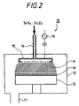
- Fig. 2 is a schematic view showing a configuration of a CVD apparatus appropriately used for embodying the present invention.
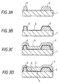
- Fig. 3A through Fig. 3D are cross sectional side views of a major part of a semiconductor device for illustrating the third embodiment of the present invention in successive processing steps.
- Fig. 4A through Fig. 4E are cross sectional side views of a major part of a semiconductor device for illustrating the fourth embodiment of the present invention in successive processing steps.
- This first embodiment is a method of forming an interlayer film according to the first aspect of the present invention and provides an interlayer film made of an SiO 2 film by two steps of film forming processes, which will be explained with reference to Figs. 1A through 1C.
- Figure 1A shows a substrate for forming an interlayer film.
- a substrate 1 is made of a silicon wafer.
- On this substrate 1 are formed an Al wiring pattern 2 and an Al pad pattern 3 via an oxide film or the like (not illustrated).
- the Al wiring pattern 2 is formed to be 0.85 ⁇ m in height and 0.4 ⁇ m in width.
- the Al pad pattern 3 is formed to be 0.85 ⁇ m in height and 100 ⁇ m in width. Between those Al wiring pattern 2 and Al pad pattern 3 is provided an enough space, with which each of those patterns becomes independent of the other.
- the wiring widths of the Al wiring pattern 2 and the Al pad pattern 3 are illustrated with different ratios for convenience.
- an SiO 2 film 4 is formed in a thickness of 0.4 ⁇ m using a well-known plasma CVD apparatus, and SiH 4 and H 2 O 2 as source materials at a film deposition temperature of 30 °C with the SiO 2 film 4 covering the Al wiring pattern 2 and the Al pad pattern 3 as shown in Fig. 1B.
- the flow rate of the source material SiH 4 was defined to be 120 sccm.
- H 2 O 2 hydrogen peroxide solution of 60% in concentration was introduced into the reduced pressure CVD apparatus at a flow rate of 0.65 g/min and instantaneously evaporated by a flasher immediately after being introduced to react to SiH 4 .
- N 2 was used as a carrier gas at a flow rate of 1000 sccm separately from the above mentioned SiH 4 and H 2 O 2 .
- the reaction pressure was set at 850 m Torr.
- SiH 4 and H 2 O 2 used as source materials satisfy a condition for having fluidity when deposited. Specifically, their fluidity is reduced at 20 °C or less under the above mentioned flow rate of source material and reaction pressure. Over 30 °C, their fluidity is almost lost. On the other hand, their fluidity is increased gradually under 20 °C. Especially, under 5 °C, their fluidity increases significantly.
- Such a deposition temperature dependent fluidity change is considered to be due to a reaction mechanism of oxidizing SiH 4 into Si(OH) 4 by an oxidant H 2 O 2 and further dehydrating and condensing the resultant Si(OH) 4 into SiO 2 , in which mechanism the process of dehydrating and condensing Si(OH) 4 nearly in liquid phase, into SiO 2 in solid phase, is accelerated at high temperatures and decelerated at low temperatures.
- the SiO 2 film 4 formed under such deposition conditions is to be as a portion of the interlayer film in this invention and, because of being formed at 30 °C, the film has almost no fluidity when deposited. Consequently, the film becomes almost even in thickness regardless of the widths of the patterns 2 and 3 formed under the film. In this stage, however, the film does not fill up the trough between the patterns 2 and 3 yet.
- the SiO 2 film 5 which is assumed as the rest portion of the interlayer film in this invention, is formed on the above mentioned SiO 2 film 4 as shown in Fig. 1C in a thickness of 0.4 ⁇ m under the same conditions except for the deposition temperature, which is changed to 0 °C.
- an interlayer film 6 comprising the SiO 2 film 4 together with the above SiO 2 film 5 is obtained.
- the SiO 2 film 5 formed under such deposition conditions has a high fluidity when deposited as mentioned above because of the deposition temperature of 0 °C, so that the film can fill up the trough formed on the SiO 2 film 4 due to the patterns 2 and 3. Consequently, the interlayer film 5 becomes to provide a satisfactory surface smoothness.
- the SiO 2 film 5 formed on this film comes in contact with the SiO 2 film 4 without coming in direct contact with the narrow Al wiring patter 2 and the wide Al pad pattern 3 even on the patterns 2 and 3.
- the underside of the SiO 2 film 5 is completely occupied with the SiO 2 film 4 which provides a uniform wettability.
- the SiO 2 film 5 is not affected by the surface tension on the patterns but is affected only by gravitation when deposited. Consequently, the film 5 can fill up the trough by the fluidity of the film and the surface become smooth.
- the difference in film thickness between the SiO 2 film on a plurality of the densely formed Al wiring patterns 2 and the SiO 2 film on a plurality of the densely formed Al pad patterns 3 could be reduced by 110 nm compared with that with the related art method in which a single step deposition process is carried out.
- this first embodiment is very effective for preventing the global smoothness from becoming poor.
- plasma exposure may be carried out onto the SiO 2 film 4 just after the first deposition process prior to the formation of the SiO 2 film 5.
- This plasma exposure hardens the plasma-exposed surface of the SiO 2 film 4, with which the film 4 loses its fluidity almost completely.
- the SiO 2 film 4 is prevented from flowing slightly to be affected by the difference in widths of patterns 2 and 3 before the second deposition process is carried out.
- This second embodiment is also a method according to the first aspect of the invention and is explained as a method of forming an interlayer film with the plasma CVD method and the reduced pressure CVD method as two steps of deposition processes.
- FIG. 2 shows an apparatus that can carry out both plasma CVD method and reduced pressure CVD method.
- This CVD apparatus 10 is provided with a wafer stage 13 in vacuum chamber 12 provided with an exhaust pipe 11 connected to a vacuum pump (not illustrated).
- a pipe 14 used for introducing source materials specifically SiH 4 , H 2 O 2 , and a carrier gas (N 2 ) from a source material supply (not illustrated).
- N 2 carrier gas
- An RF oscillator 16 is connected to this shower head 15 so that plasma is generated between this shower head 15 and the wafer stage 13.
- the wafer W is set on the wafer stage 13 as shown in Fig. 2, and in this state, the vacuum pump is started to evacuate the vacuum chamber 12 to the specified pressure. Then, the temperature of the wafer W is adjusted to 0 °C and an RF power is applied to between the shower head 15 and the wafer stage 13 by the RF oscillator 16 to generate plasma.
- the source material is then introduced into plasma P through the shower head 15 from the pipe 14 for reaction to form an SiO 2 film as shown in Fig. 1B.
- a numeral 4 is also assigned to the SiO 2 film formed in this second embodiment for convenience of the substrate explanation.
- the flow rates of SiH 4 and H 2 O 2 as source materials, as well as N 2 as a carrier gas were set to 120 sccm, 0.65 g/min, and 1000 sccm, respectively.
- the deposition pressure was set at 850 m Torr.
- the SiO 2 film 4 thus formed under such deposition conditions is assumed as a portion of the interlayer film in this invention and the film is formed with the plasma CVD method, the film does not flow when deposited. Consequently, the film becomes almost even in thickness regardless of the widths of the patterns 2 and 3 formed under the film. In this stage, however, the film cannot fill up the trough between the patterns 2 and 3 yet. Like the case in the first embodiment.
- an SiO 2 film 5 to be assumed as the rest portion of the interlayer film in this invention as shown in Fig. 1C is formed on the SiO 2 film 4 without plasma generation in a thickness of 0.4 ⁇ m under the same conditions as those of the preceding deposition.
- the interlayer film 6 comprising the SiO 2 film 4 and 5 is obtained.
- SiO 2 film 5 being deposited under a temperature of 0 °C, has high fluidity when deposited, so that it can fill up the trough formed on the surface of the SiO 2 film 4 due to the Al wiring pattern 2 and the Al pad pattern 3 like in the first embodiment. Consequently, the interlayer film 5 is formed to have a satisfactory smoothness.
- the difference in film thickness between the SiO 2 film on a plurality of the densely formed Al wiring patterns 2 and the SiO 2 film formed on a plurality of the densely formed Al pad patterns 3 could be reduced by 100 nm compared with that with the related art method in which a single step deposition process is carried out.
- this second embodiment is also very effective for preventing the global smoothness from being poor.
- SiH 4 and H 2 O 2 are used as source materials, but the materials are not limited to them in this invention.
- SiH 4 Si 2 H 6 and the like may be used, and, instead of H 2 O 2 , an oxidizer dissolved in water such as ozone (O 3 ) dissolved in water or, furthermore, liquid nitrogen and the like may be used.
- O 3 ozone
- two steps deposition process are carried out to form the desired interlayer film 6.
- the deposition process may be carried out by more than three steps for obtaining the interlayer film 6 by carrying out the first deposition process under a condition basically to reduce the fluidity or prevent the fluidization, and then the subsequent deposition processes under a condition to increase the fluidity.
- fluidity is adjusted by changing a deposition temperature which is adopted as a deposition condition to reduce or increase the fluidity.
- the fluidity may also be adjusted by changing the deposition pressure, the mixing rate of the source materials, etc.
- This third embodiment explains a method of forming an interlayer film according to the second aspect of the invention and provides the interlayer film made of an SiO 2 film on an undercoating film by two steps of film forming processes, which will be explained with reference to Figs. 3A through 3D.
- Figure 3A shows a substrate for forming an interlayer film.
- a substrate 1 is made of a silicon wafer.
- an Al wiring pattern 2 and an Al pad patter 3 via an oxide film or the like (not illustrated).
- the Al wiring pattern 2 is formed to be 0.85 ⁇ m in height and 0.4 ⁇ m in width.
- the Al pad pattern 3 is formed to be 0.85 ⁇ m in height and 100 ⁇ m in width. Between those Al wiring pattern 2 and Al pad pattern 3 is provided an enough space, with which each of those patterns becomes independent of the other.
- the wiring widths of the Al wiring pattern 2 and the Al pad pattern 3 are illustrated with different ratios for convenience.
- an undercoating film is at first formed before forming the interlayer film.
- a P-TEOS ⁇ SiO 2 film 4 (undercoating film) is deposited in a thickness of 0.1 ⁇ m with the P-TEOS ⁇ SiO 2 film 4 covering the Al wiring pattern 2 and the Al pad pattern 3 with a plasma CVD method using a well-known plasma CVD apparatus, and using TEOS (tetraethoxysilane) as a source material at a film deposition temperature of 400 °C as shown in Fig. 3B.
- this P-TEOS ⁇ SiO 2 film 4 is treated with hydroxylamine (NH 2 OH), which is a powerful reducing agent. Then, the Si-O bonds of the P-TEOS ⁇ SiO 2 film 4 are cut by the reduction treatment, so that the surface becomes hydrophobic.
- hydroxylamine NH 2 OH
- an SiO 2 film 5 (a portion of an interlayer film in this invention) with the SiO 2 film 5 covering both of the Al wiring pattern 2 and the Al pad pattern 3 as shown in Fig. 3C.
- the SiO 2 film 5 was deposited at a film-deposition temperature of 0 °C using a well-known reduced pressure CVD apparatus and using SiH 4 and H 2 O 2 as source materials so as to obtain the SiO 2 film with a thickness of 0.4 ⁇ m.
- the flow rate of the source material SiH 4 was defined to be 120 sccm.
- H 2 O 2 hydrogen peroxide solution of 60% in concentration was introduced into the reduced pressure CVD apparatus at a flow rate of 0.65 g/min and instantaneously evaporated by a flasher immediately after being introduced to react with SiH 4 .
- N 2 was used as a carrier gas at a flow rate of 1000 sccm separately from the above mentioned SiH 4 and H 2 O 2 .
- the reaction pressure was set at 850 m Torr.
- SiH 4 and H 2 O 2 used as source materials satisfy a condition for having fluidity when deposited. Specifically, their fluidity increases at 20 °C or less under the above mentioned flow rate of source material and reaction pressure. Especially, under 5 °C, their fluidity increases significantly. Above 20 °C, their fluidity decreases and over 30 °C, their fluidity is almost lost.
- the obtained SiO 2 film 5 although it intrinsically exhibits its fluidity when deposited because of being deposited at 0 °C, is prevented from exhibiting its fluidity since the hydrophobization treatment is provided in advance on the surface of the P-TEOS ⁇ SiO 2 film 4 as the undercoating film.
- the trough formed between the Al wiring pattern 2 and the Al pad pattern 3 is not yet satisfactorily filled up.
- the substrate 1 on which the SiO 2 film 5 is formed is transferred into another chamber for plasma treatment.
- the substrate 1 is heated up to 350 °C and, in this state, an oxigen plasma treatment is applied to the SiO 2 film 5 for one minute.
- an oxigen plasma treatment is applied to the SiO 2 film 5 for one minute.
- the exposed surface of the SiO 2 film 5 is hardened and loses its fluidity almost completely to prevent the SiO 2 film 5 from such slight flowing that causes the film to be affected by a difference of width between patterns 2 and 3 before the second film deposition is applied.
- this plasma exposure can also increase the hydrophilic nature of the SiO 2 film 5 itself, since the exposure eliminates fluidity of the film as well as reduces the water content in the SiO 2 film 5.
- the plasma treated substrate 1 is returned into the original chamber of the reduced pressure CVD apparatus and an SiO 2 film 6 assumed as the rest portion of the interlayer film in this invention is formed on the above mentioned SiO 2 film 5 as shown in Fig. 3D in a thickness of 0.4 ⁇ m under the same conditions as those of depositing the SiO 2 film 5 so as to obtain an interlayer film 7 comprising an SiO 2 film together with the above SiO 2 film 5.
- the SiO 2 film 6 thus formed has a high fluidity when deposited as mentioned above because of the deposition temperature of 0 °C, so that the film can fill up the trough formed on the surface of the SiO 2 film 5 due to the Al wiring patter 2 and the Al pad pattern 3. Consequently, the interlayer film 7 becomes to have a satisfactory smoothness.
- the SiO 2 film 5 to be formed on this film comes in contact with the SiO 2 film 5 without coming in contact with the P-TEOS ⁇ SiO 2 film 4 directly even on the narrow Al wiring pattern 2 and the wide Al pad pattern 3.
- the underside of the SiO 2 film 6 is completely occupied with the SiO 2 film 5 which provides a uniform wettability together with an increased hydrophilic nature due to the plasma exposure.
- the SiO 2 film 6 is not affected by the surface tension on the patterns but is affected only by gravitation when deposited. Consequently, the film 6 can fill up the troughs by the fluidity of the film and the surface becomes smooth.
- the difference in film thickness between the SiO 2 film (interlayer film 7) on a plurality of the densely formed Al wiring patterns 2 and the SiO 2 film (interlayer film 7) on a plurality of the densely formed Al pad patterns 3 could be reduced by 110 nm compared with that with the related art method in which a single step deposition process is carried out.
- this third embodiment is very effective for preventing the global smoothness from becoming poor.
- plasma exposure was carried out after the first film deposition.
- the second film deposition may be carried out without performing the plasma exposure.
- This fourth embodiment is also a method of forming an interlayer film according to the second aspect of the invention and provides the interlayer film comprising an SiO 2 film on an undercoating film by two steps of film deposition processes, which will be explained with reference to Figs. 4A through 4E.
- Figure 4A is a view showing a substrate for forming an interlayer film. Like in Fig. 1A or Fig. 3A, on the substrate 1 made of a silicon wafer are formed an Al wiring pattern 2 and an Al pad pattern 3 via an oxide film or the like (not illustrated). Since those substrate 1, Al wiring pattern 2, and Al pad pattern 3 are the same as those in Fig. 1A or Fig. 3A, detailed explanation for them will be omitted here.
- a P-TEOS ⁇ SiO 2 film 4 (undercoating film) is deposited in a thickness of 0.1 ⁇ m as shown in Fig. 3B before forming the interlayer film like the case in the third embodiment.
- a hydrogenated amorphous silicon film (a-Si: H film) 11 in a thickness of 10 nm at a deposition temperature of 300 °C with SiH 4 as a source material as shown in Fig. 4C.
- the surface of thus obtained amorphous silicon film 11 exhibits hydrophobic nature when deposited.
- this amorphous silicon film 11 is deposited an SiO 2 film (a portion of an interlayer film 12 in the invention) in a thickness of 0.4 ⁇ m, covering the Al wiring pattern 2 and the Al pad pattern 3 as shown in Fig. 4D.
- the deposition of this SiO 2 film 12 is carried out under the same conditions as those of the SiO 2 film 5 in the first embodiment.
- SiO 2 film 12 is prevented from exhibiting its fluidity since the surface of the amorphous silicon film 11 deposited on the P-TEOS ⁇ SiO 2 film 4 as an undercoating film in advance exhibits hydrophobic nature. This makes the SiO 2 film 12 almost even in thickness regardless of the widths of the Al wiring pattern 2 and the Al pad pattern 3. Consequently, the SiO 2 film 12 formed as a portion of an interlayer film in this invention is prevented from exhibiting its fluidity like the case in the third embodiment to have poor smoothness. Thus, the trough formed between the Al wiring pattern 2 and the Al pad pattern 3 is not yet satisfactorily filled up in this stage.
- the substrate 1 on which the SiO 2 film 12 is formed is transferred into another chamber for plasma treatment.
- the substrate 1 is heated up to 350 °C and, in this state, an oxigen plasma treatment is applied to the SiO 2 film 12 for one minute.
- the plasma treated substrate 1 is returned into the original chamber of the reduced pressure CVD apparatus and an SiO 2 film 13 assumed as the rest portion of the interlayer film in this invention is formed on the above mentioned SiO 2 film 12 as shown in Fig. 4E under the same conditions as those of depositing the SiO 2 film 12 in a thickness of 0.4 ⁇ m to obtain an interlayer film 14 comprising the SiO 2 film together with the above SiO 2 film 12.
- SiO 2 film 13 being deposited under a temperature of 0 °C so as to have high fluidity when deposited, can fill up the trough formed on the surface of the SiO 2 film 12 due to the Al wiring pattern 2 and the Al pad pattern 3 like the case in the third embodiment. Consequently, the interlayer film 14 is formed to have a satisfactory smoothness.
- the SiO 2 film 13 to be formed on the film 12 comes in contact with the SiO 2 film 12 without coming in contact with the amorphous silicon film 11 directly even on the narrow Al wiring pattern 2 and the wide Al pad pattern 3.
- the SiO 2 film 13 is completely occupied with the SiO 2 film 12 thereunder which provides a uniform wettability together with an increased hydrophilic nature due to the plasma exposure. Consequently, unlike the prior art method, the film 13 is not affected by the surface tension on the patterns when deposited and accordingly the film 13 can be filled in the troughs due to its fluidity to be smoothed like the case in the first embodiment.
- the difference in film thickness between the SiO 2 film (interlayer film 14) on a plurality of the densely formed Al wiring patterns 2 and the SiO 2 film (interlayer film 14) on a plurality of the densely formed Al pad patterns 3 could be reduced by 110 nm compared with that with the related art method in which a single step deposition process is carried out.
- this second embodiment is also very effective for preventing the global smoothness from being poor.
- plasma exposure was carried out after the first film deposition, but the second film deposition may be carried out without performing the plasma exposure.
- a similarly hydrophobic polysilicon film may be deposited on the P-TEOS ⁇ SiO 2 film 4.
- This fifth embodiment is also a method of forming an interlayer film according to the second aspect of the invention and provides the interlayer film comprising an SiO 2 film on an undercoating film by two steps film deposition process. It is different from the third embodiment shown in Figs. 3A through 3D in that the SiO 2 film 5 is formed after the formation of the P-TEOS ⁇ SiO 2 film 4 as a hydrophobic undercoating film with the hydrophobic nature of the formed P-TEOS ⁇ SiO 2 film 4 being retained, instead of carrying out the reduction treatment for the film 4.
- the substrate 1 is transferred into a chamber of the reduced pressure CVD apparatus with the vacuum pressure in depositing the P-TEOS ⁇ SiO 2 film 4 being maintained so that the hydrophobic nature of the P-TEOS ⁇ SiO 2 film 4 is retained. Then, the P-TEOS ⁇ SiO 2 film 4, which becomes hydrophobic due to many dangling bonds (unjoined bonds) existing on the surface immediately after the deposition, can retain its hydrophobic nature because the substrate 1 is held in vacuum while being transferred into a chamber of the reduced pressure CVD apparatus.
- the SiO 2 film 5 being formed under the same conditions as those in the case shown in Fig. 3C with the P-TEOS ⁇ SiO 2 film 4 thus retaining its hydrophobic property, is prevented from exhibiting its fluidity and accordingly the film thickness becomes almost even regardless of the widths of the Al wiring pattern 2 and the Al pad pattern 3.
- the SiO 2 film 5 has poor smoothness and accordingly does not fill up the trough between the Al wiring patter 2 and the Al pad pattern 3 yet in this stage.
- the surface of the SiO 2 film 5 is exposed to a plasma like in the first embodiment, and then the SiO 2 film 6 is formed in a thickness of 0.4 ⁇ m under the same film deposition conditions as those in the first embodiment to obtain an interlayer film 7.
- SiO 2 film 6 being deposited at a temperature of 0 °C so as to increase its fluidity, can fill up the trough formed between the Al wiring pattern 2 and the Al pad pattern 3 on the surface of the SiO 2 film 5 like the case in the third embodiment. Consequently, the interlayer film 7 is formed to have a satisfactory smoothness.
- the SiO 2 film 6 to be formed on the film 5 comes in contact with the SiO 2 film 5 without coming in contact with the P-TEOS ⁇ SiO 2 film 4 directly even on the narrow Al wiring pattern 2 and the wide Al pad pattern 3.
- the underside of the SiO 2 film 6 is completely occupied with the SiO 2 film 5 which provides a uniform wettability together with an increased hydrophilic nature due to the plasma exposure. Therefore, unlike the related art method, the film 6 is not affected by the surface tension on the patterns when deposited and, like the case in the third embodiment, the film 6 can fill up the troughs due to its fluidity to smooth the surface.
- the difference in film thickness between the SiO 2 film (interlayer film 7) on a plurality of the densely formed Al wiring patterns 2 and the SiO 2 film (interlayer film 7) formed on a plurality of the densely formed Al pad patterns 3 could be reduced by 120 nm compared with that with the related art method in which a single step deposition process is carried out.
- this fifth embodiment is also very effective for preventing the global smoothness from becoming poor.
- plasma exposure was carried out after the first film deposition, but the second film deposition may be carried out without performing the plasma exposure.
- SiH 4 and H 2 O 2 are used as source materials, but the materials are not limited to them in this invention.
- SiH 4 Si 2 H 6 and the like may be used, and, instead of H 2 O 2 , an oxidizer dissolved in water such as ozone (O 3 ) dissolved in water or, furthermore, oxigen and the like may be used.
- O 3 ozone
- the obtained film (a portion of an interlayer film) becomes almost even in thickness regardless of the widths of patterns. Furthermore, since the rest portion of the interlayer film is formed on this film under a condition to increase the fluidity when deposited, this rest portion fills up the trough between patterns. Consequently, the interlayer film comprising the above mentioned portion of the interlayer film and this rest portion becomes to have satisfactory smoothness even on patterns of differing widths.
- an undercoating film is formed on the surface of a substrate, then a portion of an interlayer film is formed after the undercoating film is reduction treated so as to become hydrophobic or after a polysilicon film or an amorphous silicon film is deposited on the undercoating film, or with the hydrophobic nature of the undercoating film being retained, so that the obtained film (a portion of the interlayer film) becomes almost even in thickness regardless of the widths of wiring patterns. And, since the rest portion of the interlayer film is formed on this film, the rest portion fills up the trough between wiring patterns, with which the interlayer film comprising the above mentioned portion and this rest portion becomes to have satisfactory smoothness even on wiring patterns of differing widths.
Landscapes
- Internal Circuitry In Semiconductor Integrated Circuit Devices (AREA)
Applications Claiming Priority (4)
| Application Number | Priority Date | Filing Date | Title |
|---|---|---|---|
| JP19064196A JP3491451B2 (ja) | 1996-07-19 | 1996-07-19 | 層間膜の形成方法 |
| JP190641/96 | 1996-07-19 | ||
| JP216996/96 | 1996-08-19 | ||
| JP21699696A JPH1064998A (ja) | 1996-08-19 | 1996-08-19 | 層間膜の形成方法 |
Publications (2)
| Publication Number | Publication Date |
|---|---|
| EP0820095A2 true EP0820095A2 (de) | 1998-01-21 |
| EP0820095A3 EP0820095A3 (de) | 1999-01-27 |
Family
ID=26506226
Family Applications (1)
| Application Number | Title | Priority Date | Filing Date |
|---|---|---|---|
| EP97111871A Withdrawn EP0820095A3 (de) | 1996-07-19 | 1997-07-11 | Herstellungsverfahren für eine Zwischenschicht |
Country Status (2)
| Country | Link |
|---|---|
| US (5) | US5888909A (de) |
| EP (1) | EP0820095A3 (de) |
Cited By (1)
| Publication number | Priority date | Publication date | Assignee | Title |
|---|---|---|---|---|
| EP0939433A3 (de) * | 1998-02-12 | 2000-08-30 | Canon Sales Co., Inc. | Verfahren zur Reformierung der Oberfläche von einer Grundierschicht und Herstellungsverfahren von einer Halbleitervorrichtung |
Families Citing this family (8)
| Publication number | Priority date | Publication date | Assignee | Title |
|---|---|---|---|---|
| EP0820095A3 (de) * | 1996-07-19 | 1999-01-27 | Sony Corporation | Herstellungsverfahren für eine Zwischenschicht |
| JPH1126449A (ja) * | 1997-06-30 | 1999-01-29 | Sony Corp | 絶縁膜の成膜方法 |
| US6013134A (en) * | 1998-02-18 | 2000-01-11 | International Business Machines Corporation | Advance integrated chemical vapor deposition (AICVD) for semiconductor devices |
| GB0118417D0 (en) * | 2001-07-28 | 2001-09-19 | Trikon Holdings Ltd | A method of depositing a dielectric film |
| US9541977B1 (en) | 2001-08-28 | 2017-01-10 | Eugene M. Lee | Computer-implemented method and system for automated claim charts with context associations |
| BRPI0308319B1 (pt) | 2002-03-11 | 2015-06-09 | Beaver Visitec Int Us Inc | Método para fabricar um dispositivo de corte de material cristalino e método para fabricar uma lâmina cirúrgica de material cristalino |
| US20070202636A1 (en) * | 2006-02-22 | 2007-08-30 | Applied Materials, Inc. | Method of controlling the film thickness uniformity of PECVD-deposited silicon-comprising thin films |
| JP2011014872A (ja) * | 2009-06-04 | 2011-01-20 | Tokyo Electron Ltd | アモルファスカーボン膜の形成方法および形成装置 |
Family Cites Families (24)
| Publication number | Priority date | Publication date | Assignee | Title |
|---|---|---|---|---|
| JP2631659B2 (ja) * | 1987-07-09 | 1997-07-16 | 富士通株式会社 | 半導体装置 |
| JPH0373539A (ja) * | 1989-08-11 | 1991-03-28 | Ricoh Co Ltd | アーリー電圧の高い横型バイポーラトランジスタの製造方法 |
| US5132774A (en) * | 1990-02-05 | 1992-07-21 | Mitsubishi Denki Kabushiki Kaisha | Semiconductor device including interlayer insulating film |
| JPH0719777B2 (ja) * | 1990-08-10 | 1995-03-06 | 株式会社半導体プロセス研究所 | 半導体装置の製造方法 |
| JPH04158551A (ja) * | 1990-10-22 | 1992-06-01 | Seiko Epson Corp | 半導体装置の製造方法 |
| EP0497541A1 (de) * | 1991-01-28 | 1992-08-05 | Kawasaki Steel Corporation | Halbleiterbauelement mit einer Bor-Phosphorsilikat-Glasschicht und ihr Herstellungsverfahren |
| JPH05259297A (ja) * | 1992-03-09 | 1993-10-08 | Oki Electric Ind Co Ltd | 半導体素子の製造方法 |
| US5576247A (en) * | 1992-07-31 | 1996-11-19 | Matsushita Electric Industrial Co., Ltd. | Thin layer forming method wherein hydrophobic molecular layers preventing a BPSG layer from absorbing moisture |
| JP2684942B2 (ja) * | 1992-11-30 | 1997-12-03 | 日本電気株式会社 | 化学気相成長法と化学気相成長装置および多層配線の製造方法 |
| JP2779996B2 (ja) * | 1993-02-25 | 1998-07-23 | 日本電信電話株式会社 | 半導体装置の製造方法 |
| JPH0729897A (ja) * | 1993-06-25 | 1995-01-31 | Nec Corp | 半導体装置の製造方法 |
| US5448111A (en) * | 1993-09-20 | 1995-09-05 | Fujitsu Limited | Semiconductor device and method for fabricating the same |
| EP0653501B1 (de) * | 1993-11-11 | 1998-02-04 | Nissin Electric Company, Limited | Plasma-CVD-Verfahren und Vorrichtung |
| US5453406A (en) * | 1994-06-13 | 1995-09-26 | Industrial Technology Research Institute | Aspect ratio independent coating for semiconductor planarization using SOG |
| JPH08148559A (ja) * | 1994-11-15 | 1996-06-07 | Fujitsu Ltd | 絶縁膜を有する半導体装置の製造方法 |
| JPH08181210A (ja) * | 1994-12-26 | 1996-07-12 | Toshiba Corp | 半導体装置の製造方法 |
| JPH08181276A (ja) * | 1994-12-26 | 1996-07-12 | Toshiba Corp | 半導体装置の製造方法 |
| JP3281209B2 (ja) * | 1995-01-30 | 2002-05-13 | 株式会社東芝 | 半導体装置の製造方法 |
| US5703344A (en) * | 1995-06-30 | 1997-12-30 | Visa International Service Association | Electronic funds confirmation at point of transaction |
| JP3149739B2 (ja) * | 1995-07-14 | 2001-03-26 | ヤマハ株式会社 | 多層配線形成法 |
| JP3070450B2 (ja) * | 1995-07-14 | 2000-07-31 | ヤマハ株式会社 | 多層配線形成法 |
| JPH09116011A (ja) * | 1995-10-23 | 1997-05-02 | Mitsubishi Electric Corp | 半導体装置およびその製造方法 |
| EP0820095A3 (de) * | 1996-07-19 | 1999-01-27 | Sony Corporation | Herstellungsverfahren für eine Zwischenschicht |
| US5691247A (en) * | 1996-12-19 | 1997-11-25 | Tower Semiconductor Ltd. | Method for depositing a flow fill layer on an integrated circuit wafer |
-
1997
- 1997-07-11 EP EP97111871A patent/EP0820095A3/de not_active Withdrawn
- 1997-07-18 US US08/896,542 patent/US5888909A/en not_active Expired - Lifetime
-
1998
- 1998-06-30 US US09/107,712 patent/US6048801A/en not_active Expired - Lifetime
-
1999
- 1999-03-04 US US09/262,255 patent/US6136726A/en not_active Expired - Lifetime
- 1999-03-04 US US09/262,619 patent/US6221756B1/en not_active Expired - Lifetime
- 1999-03-08 US US09/265,232 patent/US6232245B1/en not_active Expired - Lifetime
Cited By (2)
| Publication number | Priority date | Publication date | Assignee | Title |
|---|---|---|---|---|
| EP0939433A3 (de) * | 1998-02-12 | 2000-08-30 | Canon Sales Co., Inc. | Verfahren zur Reformierung der Oberfläche von einer Grundierschicht und Herstellungsverfahren von einer Halbleitervorrichtung |
| US6225236B1 (en) | 1998-02-12 | 2001-05-01 | Canon Sales Co., Inc. | Method for reforming undercoating surface and method for production of semiconductor device |
Also Published As
| Publication number | Publication date |
|---|---|
| US6232245B1 (en) | 2001-05-15 |
| US5888909A (en) | 1999-03-30 |
| US6136726A (en) | 2000-10-24 |
| US6221756B1 (en) | 2001-04-24 |
| EP0820095A3 (de) | 1999-01-27 |
| US6048801A (en) | 2000-04-11 |
Similar Documents
| Publication | Publication Date | Title |
|---|---|---|
| EP1316108B9 (de) | Herstellungsprozess eines halbleiterbauelements mit einem zwischenfilm aus siliziumnitrid mit niedriger dielektrizitätskonstante | |
| US7205248B2 (en) | Method of eliminating residual carbon from flowable oxide fill | |
| US7001850B2 (en) | Method of depositing dielectric films | |
| US4617087A (en) | Method for differential selective deposition of metal for fabricating metal contacts in integrated semiconductor circuits | |
| KR100227287B1 (ko) | 매립 도전층 및 그 형성방법 | |
| US5246887A (en) | Dielectric deposition | |
| US6297171B1 (en) | Semiconductor processing method of promoting photoresist adhesion to an outer substrate layer predominately comprising silicon nitride | |
| US20030148020A1 (en) | Method of depositing low dielectric constant silicon carbide layers | |
| US6136690A (en) | In situ plasma pre-deposition wafer treatment in chemical vapor deposition technology for semiconductor integrated circuit applications | |
| GB2307788A (en) | Method for forming field oxide in semiconductor device | |
| US5567661A (en) | Formation of planarized insulating film by plasma-enhanced CVD of organic silicon compound | |
| EP0288754A2 (de) | CVD-Verfahren mit hohem Nutzeffekt für Wolfram für spannungsfreie Schichten | |
| US6232245B1 (en) | Method of forming interlayer film | |
| KR100292393B1 (ko) | 반도체장치및그제조방법 | |
| US6713386B1 (en) | Method of preventing resist poisoning in dual damascene structures | |
| US6090705A (en) | Method of eliminating edge effect in chemical vapor deposition of a metal | |
| KR100256818B1 (ko) | 반도체소자의 소자분리막 형성방법 | |
| KR20000026975A (ko) | 반도체 장치의 제조 방법 | |
| JP3491451B2 (ja) | 層間膜の形成方法 | |
| KR0144080B1 (ko) | 층덮힘이 개선된 절연막을 형성하기 위한 화학기상증착 방법 | |
| JP2598524B2 (ja) | ドライエッチング方法 | |
| US6232246B1 (en) | Method of fabricating semiconductor device | |
| US20030219961A1 (en) | Method to reduce reflectivity of polysilicon layer | |
| KR100486235B1 (ko) | 도핑되지않은실리콘유리(usg)막의형성방법 | |
| JPH1064998A (ja) | 層間膜の形成方法 |
Legal Events
| Date | Code | Title | Description |
|---|---|---|---|
| PUAI | Public reference made under article 153(3) epc to a published international application that has entered the european phase |
Free format text: ORIGINAL CODE: 0009012 |
|
| AK | Designated contracting states |
Kind code of ref document: A2 Designated state(s): DE GB |
|
| AX | Request for extension of the european patent |
Free format text: AL;LT;LV;RO;SI |
|
| PUAL | Search report despatched |
Free format text: ORIGINAL CODE: 0009013 |
|
| AK | Designated contracting states |
Kind code of ref document: A3 Designated state(s): AT BE CH DE DK ES FI FR GB GR IE IT LI LU MC NL PT SE |
|
| AX | Request for extension of the european patent |
Free format text: AL;LT;LV;RO;SI |
|
| 17P | Request for examination filed |
Effective date: 19990629 |
|
| AKX | Designation fees paid |
Free format text: DE GB |
|
| STAA | Information on the status of an ep patent application or granted ep patent |
Free format text: STATUS: THE APPLICATION HAS BEEN WITHDRAWN |
|
| 18W | Application withdrawn |
Effective date: 20021211 |