EP0820100A2 - Halbleiterbauteil und dessen Herstellungsverfahren, Grundzellenbibliothek und deren Herstellungsverfahren und Maske - Google Patents
Halbleiterbauteil und dessen Herstellungsverfahren, Grundzellenbibliothek und deren Herstellungsverfahren und Maske Download PDFInfo
- Publication number
- EP0820100A2 EP0820100A2 EP97111750A EP97111750A EP0820100A2 EP 0820100 A2 EP0820100 A2 EP 0820100A2 EP 97111750 A EP97111750 A EP 97111750A EP 97111750 A EP97111750 A EP 97111750A EP 0820100 A2 EP0820100 A2 EP 0820100A2
- Authority
- EP
- European Patent Office
- Prior art keywords
- basic cell
- basic
- wiring pattern
- dummy wiring
- cell
- Prior art date
- Legal status (The legal status is an assumption and is not a legal conclusion. Google has not performed a legal analysis and makes no representation as to the accuracy of the status listed.)
- Withdrawn
Links
Images





Classifications
-
- H—ELECTRICITY
- H10—SEMICONDUCTOR DEVICES; ELECTRIC SOLID-STATE DEVICES NOT OTHERWISE PROVIDED FOR
- H10D—INORGANIC ELECTRIC SEMICONDUCTOR DEVICES
- H10D84/00—Integrated devices formed in or on semiconductor substrates that comprise only semiconducting layers, e.g. on Si wafers or on GaAs-on-Si wafers
- H10D84/90—Masterslice integrated circuits
- H10D84/903—Masterslice integrated circuits comprising field effect technology
-
- H—ELECTRICITY
- H10—SEMICONDUCTOR DEVICES; ELECTRIC SOLID-STATE DEVICES NOT OTHERWISE PROVIDED FOR
- H10D—INORGANIC ELECTRIC SEMICONDUCTOR DEVICES
- H10D89/00—Aspects of integrated devices not covered by groups H10D84/00 - H10D88/00
- H10D89/10—Integrated device layouts
-
- G—PHYSICS
- G03—PHOTOGRAPHY; CINEMATOGRAPHY; ANALOGOUS TECHNIQUES USING WAVES OTHER THAN OPTICAL WAVES; ELECTROGRAPHY; HOLOGRAPHY
- G03F—PHOTOMECHANICAL PRODUCTION OF TEXTURED OR PATTERNED SURFACES, e.g. FOR PRINTING, FOR PROCESSING OF SEMICONDUCTOR DEVICES; MATERIALS THEREFOR; ORIGINALS THEREFOR; APPARATUS SPECIALLY ADAPTED THEREFOR
- G03F1/00—Originals for photomechanical production of textured or patterned surfaces, e.g., masks, photo-masks, reticles; Mask blanks or pellicles therefor; Containers specially adapted therefor; Preparation thereof
- G03F1/36—Masks having proximity correction features; Preparation thereof, e.g. optical proximity correction [OPC] design processes
Definitions
- This invention relates to a semiconductor device having a semiconductor integrated circuit laid out on a semiconductor substrate based on a basic cell library having basic cells of novel structure and a method for manufacturing the same.
- a semiconductor device is manufactured basically via a design process (function design, logic design, layout design and the like) and a manufacturing and test process (chip manufacturing process, test evaluation process and the like).
- the design process is effected in an order of function design ⁇ logic design ⁇ layout design.
- the process technology of the semiconductor device enters upon the deep submicron generation.
- the width of wirings used in the semiconductor device is reduced to 0.3 ⁇ m or less.
- a reduction in the wiring width of the polysilicon wiring (which is hereinafter referred to as the poly-width) or the like causes a problem that a minute variation in the polywidth caused by the optical proximity effect cannot be neglected.
- the optical proximity effect is a phenomenon that the finish value of the poly-width W of the polysilicon wiring will vary according to a space d between the polysilicon wiring and an adjacent polysilicon wiring (which is hereinafter referred to as a poly-space). That is, the size of the pattern in the semiconductor device is reduced and the integration density thereof is enhanced, and a charged beam exposure device or an optical stepper is used to draw and expose the pattern, but at this time, the dimensional precision of the pattern is lowered by the optical proximity effect.
- FIGS. 1A and 1B are a plan view of a polysilicon wiring pattern and a characteristic diagram for illustrating the dependency of the wiring width on the space between the wirings which varies by the optical proximity effect.
- the ordinate indicates the poly-width W ( ⁇ m)
- the abscissa indicates the poly-space d ( ⁇ m).
- the poly-width W is reduced to approx. 0.26 ⁇ m when the poly-space d becomes approx. 1 ⁇ m. Therefore, at the time of manufacturing the semiconductor device, it becomes absolutely necessary to make correction in order to enhance the dimensional precision of the pattern which is lowered by the optical proximity effect when the pattern for wirings or the like to be formed on the semiconductor device is drawn or exposed.
- OPC Optical Proximity effect Correction
- the OPC technique is a technique for keeping the finish value of the poly-width after exposure at a constant value by estimating an amount of variation in the poly-width due to the optical proximity effect of the polysilicon wirings based on the distance between the polysilicon wiring and an adjacent polysilicon wiring pattern in close proximity thereto and previously correcting the mask value of a photoresist for forming the polysilicon wiring to cancel the variation amount.
- the polysilicon wiring pattern is not standardized, the poly-space is different depending on polysilicon wirings of the whole chip, and therefore, it is necessary to make corrections by the OPC technique for all of the polysilicon wirings on the chip.
- FIG. 2A shows an A cell registered in the basic cell library and one pair of diffusion regions 2 acting as source/drain regions are formed in a cell frame 1 in which a cell region is formed.
- the diffusion regions 2 include a p+ diffusion region 21 and an n+ diffusion region 22 and one polysilicon gate 3 is disposed to extend over the diffusion regions 21, 22.
- FIG. 2B shows a B cell registered in the basic cell library and two polysilicon gates 3 are disposed to extend over a p+ diffusion region 21 and n+ diffusion region 22.
- FIG. 2A shows an A cell registered in the basic cell library and one pair of diffusion regions 2 acting as source/drain regions are formed in a cell frame 1 in which a cell region is formed.
- the diffusion regions 2 include a p+ diffusion region 21 and an n+ diffusion region 22 and one polysilicon gate 3 is disposed to extend over the diffusion regions 21, 22.
- FIG. 2B shows a B cell registered in the basic cell library and two polysilicon gates 3 are disposed to extend over a
- FIG. 2C shows a C cell registered in the basic cell library and three polysilicon gates 3 are disposed to extend over a p+ diffusion region 21 and n+ diffusion region 22.
- FIG. 3 shows an E cell registered in the basic cell library and three polysilicon gates 3 are disposed to selectively extend over p+ diffusion regions 211, 221 and n+ diffusion regions 212, 222.
- FIGS. 4 and 5 are plan views of chips on which standard cells are laid out.
- basic cells A, B, C registered in the basic cell library are placed.
- the basic cells A, B, C are successively placed in an order of ABC in a preset portion of the chip.
- the basic cells are successively placed in an order of CBA in a preset portion of the chip.
- D target polysilicon gate
- E, F polysilicon gate
- the poly-data D is disposed in close proximity to the proximity poly-data E.
- the proximity poly-data E is bent and a poly-space b1 between the poly-data D and a portion of the proximity poly-data E which is formed above the diffusion region 21 is larger than a poly-space b2 between the poly-data D and a portion of the proximity poly-data E which is formed above the diffusion region 22.
- the poly-data D is disposed in close proximity to the proximity poly-data F. Poly-spaces between the poly-data D and both end portions of the proximity poly-data F are b3 and b4. Therefore, if b2, b3 and b4 are set equal to each other, the poly-space b1 becomes larger than b4 (b1 > b4).
- the distance between the poly-data and the proximity poly-data is different depending on a difference in the placement of the basic cells on the chip.
- FIG. 6 is a plan view of a basic cell for illustrating the mask value correction for a variation due to the optical proximity effect.
- the poly-width of the poly-data G on the mask is increased (increased width c) while monitoring the relation between the poly-width of the poly-data G and the poly-space b.
- the poly-width is changed according to the distance b to the adjacent poly-data.
- the wiring pattern is formed in the chip forming process by use of a mask which has been subjected to the correction process for the optical proximity effect.
- the poly-datas which should be corrected by the OPC technique lie only in the cell region as shown in FIG. 6. Therefore, if the polywidth is corrected by the OPC technique not in the whole portion of the chip but in the respective cell regions, the number of poly-datas subjected to the OPC process is significantly reduced and the amount of processing is reduced.
- the distance from the poly-data used in the cell to the proximity poly-data is not definite inside the cell, and only when the standard cell is laid out on the chip, the distance from a preset poly-data (polysilicon gate) to an adjacent poly-data (proximity poly-data) is determined.
- This invention has been made to solve the above problem, and an object of this invention is to provide a semiconductor device capable of reducing the amount of the poly-data to be corrected by the OPC technique, reducing the CAD processing time and reducing the product TAT by performing correction by the OPC technique for each cell, a basic cell library for realizing the semiconductor device, a method for manufacturing the semiconductor device, a method for forming the basic cell library, and a mask for manufacturing the semiconductor device.
- This invention is characterized in that a poly-data which is the dummy wiring pattern of a polysilicon wiring pattern is additionally formed along the periphery of a basic cell in the semiconductor device. That is, the basic cell registered in the basic cell library is characterized in that the dummy wiring pattern is previously formed along the periphery thereof. With this structure, the distance between the polysilicon gate used in the circuit and a polysilicon wiring of the dummy wiring pattern formed in close proximity thereto in the basic cell can be determined in the cell.
- the correction value by the OPC technique on the mask used for correcting the gate width based on the variation amount of the poly-width can be determined only inside the cell. Further, the correction can be previously performed not for each product but for each cell.
- the poly-width correction process effected for the optical proximity effect after the cell placement in the design process containing a continuous process of function design ⁇ logic design ⁇ layout design can be omitted.
- the basic cell library is corrected by the OPC process before the cells of the product (chip) are placed, it is not necessary to perform the OPC process at the time of development of the product, the delay in the TAT caused by correction by the OPC technique for each product can be prevented, and a mask for the optimum polysilicon wiring pattern can be easily formed. Further, since the correction value of each poly-data in the basic cell is not dependent on the poly-data of the adjacent cell and is determined by the poly-data in the basic cell, it is sufficient only if the correction is performed once for each basic cell and the correction processing data amount can be made smaller than in a case wherein the correction is performed for the whole portion of the chip.
- This invention described in claim 1 is characterized by including at least one basic cell having a dummy cell pattern placed on the peripheral portion thereof in a semiconductor device.
- a basic cell library of this invention described in claim 17 is characterized in that at least one basic cell having a dummy wiring pattern is formed.
- a method for forming a basic cell library of this invention described in claim 22 is characterized by including a step of preparing a first basic cell of first layout structure for realizing a plurality of basic gates on a semiconductor substrate, and a step of forming a second basic cell by placing a dummy wiring pattern on the peripheral portion of the first basic cell.
- a method for manufacturing a semiconductor device of this invention described in claim 25 is characterized by including a step of preparing a first basic cell of layout structure for realizing a plurality of basic gates on a semiconductor substrate, a step of forming a second basic cell by forming a dummy wiring pattern on the region boundary of the first basic cell, and a step of laying out a semiconductor integrated circuit on the semiconductor substrate by using the second basic cell.
- a method for manufacturing a semiconductor device of this invention described in claim 27 is characterized by including a step of preparing plural types of basic cells having dummy wiring patterns formed along the region boundaries thereof, and a step of selecting at least two basic cells from the plural types of basic cells, overlapping parts of the dummy wiring patterns of the selected basic cells to form a new basic cell, and stocking the new basic cell in the basic cell layout library.
- a mask of this invention described in claim 28 is characterized in that at least one basic cell portion having a dummy wiring pattern arranged on the peripheral portion thereof is formed.
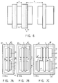
- FIGS. 7A, 7B, 7C and FIG. 8 are plan views showing basic cells registered in the basic cell library of this invention.
- the basic cell library basic cells used for constructing a semiconductor integrated circuit are registered, and at the time of manufacturing a semiconductor device, the basic cells registered in the basic cell library are adequately selected to make a layout design for forming a logic circuit.
- the basic cells of this invention shown in the above drawing are used for laying out a standard cell type semiconductor device.
- the basic cell has a layout structure for realizing a plurality of basic gates on a substrate and is constructed by an internal wiring such as a gate, diffusion regions and a dummy wiring pattern which is the important factor of this invention.
- the basic cell includes an inverter, 2-input NAND, flip-flop, EX-OR, AND, NOR and is a layout structure for realizing a basic gate on the semiconductor substrate.
- FIG. 7A shows an A cell registered in the basic cell library.
- a dummy wiring pattern 4 of a polysilicon wiring pattern is formed along the cell frame which defines a cell region. That is, the cell region is surrounded by the dummy wiring pattern 4.
- one pair of diffusion regions (SDG) 2 used as source/drain regions are formed.
- the diffusion regions 2 include a p+ diffusion region 21 and n+ diffusion region 22 and one polysilicon gate 3 is formed to extend over the diffusion regions 21, 22.
- the gate width w1 of the polysilicon gate 3 and the pattern width w2 of the dummy wiring pattern 4 are both set to 0.3 ⁇ m, for example.
- the dummy wiring pattern 4 is formed of portions 41 which are parallel to the polysilicon gate 3 and portions 42 which are perpendicular to the polysilicon gate 3.
- FIG. 7B shows a B cell registered in the basic cell library, and two polysilicon gates 3 are each formed to extend over the p+ diffusion region 21 and n+ diffusion region 22.
- a dummy wiring pattern 4 of a polysilicon wiring pattern having the same width as the gate width of the polysilicon gate is formed to surround a cell region.
- the dummy wiring pattern 4 is formed of portions 41 which are parallel to the polysilicon gate 3 and portions 42 which are perpendicular to the polysilicon gate 3.
- FIG. 7C shows a C cell registered in the basic cell library, and three polysilicon gates 3 are each formed to extend over the p+ diffusion region 21 and n+ diffusion region 22.
- a dummy wiring pattern 4 of a polysilicon wiring pattern having the same width as the gate width of the polysilicon gate is formed to surround a cell region.
- the dummy wiring pattern 4 is formed of portions 41 which are parallel to the polysilicon gate 3 and portions 42 which are perpendicular to the polysilicon gate 3.
- FIG. 8 shows an E cell registered in the basic cell library.
- a dummy wiring pattern 4 of a polysilicon wiring pattern is formed along the cell frame which defines a cell region. In the cell region, diffusion regions 2 are formed.
- the diffusion regions 2 include p+ diffusion region 211, 221 and n+ diffusion regions 212, 222, one polysilicon gate 3 is formed to extend over the diffusion regions 211, 212, and two polysilicon gates 3 are each formed to extend over the diffusion regions 221, 222.
- the gate width of the polysilicon gate 3 and the pattern width of the dummy wiring pattern 4 are both set to 0.3 ⁇ m, for example.
- the dummy wiring pattern 4 is formed of portions which are parallel to the polysilicon gate 3 and portions which are perpendicular to the polysilicon gate 3.
- the parallel portion causes a variation in the gate width due to the optical proximity effect in the polysilicon gate 3, but since the distance between the polysilicon gate 3 and the dummy wiring pattern 4 is constant, correction can be previously made in the state of basic cell if a variation in the gate width occurs in the polysilicon gate 3.
- basic cells are selected from the basic cell library and laid out on the chip.
- the design process is completed by laying out the basic cells such as the A cell, B cell, C cell, E cell shown in FIGS. 7A, 7B, 7C and FIG. 8 on the chip and then the chip forming process is started. Since it is not necessary to newly form a dummy wiring pattern for correcting a variation due to the optical proximity effect at the time of change of the process, the process can be simplified.
- the dummy wiring pattern of this invention can effectively cope with this compensation.
- the dummy wiring pattern forming process for compensating for the optical proximity effect effected after the layout design can be omitted. That is, since the basic cell library is subjected to correction by the OPC technique before the cells of the product (chip) are placed, it is not necessary to effect the OPC process at the time of development of the product, the delay in the TAT caused by correction by the OPC technique for each product can be prevented, and an optimum mask of the polysilicon wiring pattern can be easily formed.
- FIG. 9 is a plan view showing part of a mask formed by use of the basic cell of FIG. 8. Also, in the following embodiments, the mask is formed in the same manner as described above.
- each polysilicon wiring pattern in the basic cell is determined by the poly-data in the basic cell, it is sufficient only if the correction is performed once for each basic cell and the correction processing data amount can be made smaller than in a case wherein the correction is performed for the whole portion of the chip.
- FIG. 10 is a plan view of a basic cell registered in the basic cell library.
- the basic cell (D cell) shown in FIG. 10 is used for the layout of a standard cell type semiconductor device.
- the D cell is constructed by combining the A cell, B cell and C cell of the basic cell library shown in FIGS. 7A, 7B and 7C.
- the basic cell is formed of a combination of the cells placed in an order of ABC, but can be formed of a combination of the cells placed in an order of BAC, CAB, ACB, BCA, CBA, and the basic cells thus formed are registered as different basic cells in the basic cell library. Further, structures obtained by placing desired two of the A, B and C regions in desired combinations are registered as basic cells in the basic cell library.
- the dummy wiring pattern is formed on the peripheral portion of the original basic cell for each original basic cell.
- the A, B and C regions are respectively correspond to the original A cell, B cell and C cell. Therefore, the portion 41 which is parallel to the polysilicon gate 3 of the dummy wiring pattern 4 is formed between the regions. Further, the dummy wiring pattern 4 of a polysilicon wiring pattern is formed along the cell frame which defines a cell region. That is, the cell region is surrounded by the dummy wiring pattern 4.
- one pair of diffusion regions (SDG) 2 used as source/drain regions are formed in each of the A, B, C regions.
- the diffusion regions 2 include a p+ diffusion region 21 and an n+ diffusion region 22 and one to three polysilicon gates 3 are each formed to extend over the diffusion regions 21, 22.
- the gate width of the polysilicon gate 3 and the pattern width of the dummy wiring pattern 4 are both set to 0.3 ⁇ m, for example.
- the dummy wiring pattern 4 is formed of portions 41 which are parallel to the polysilicon gate 3 and portions 42 which are perpendicular to the polysilicon gate 3.
- the parallel portion 41 causes a variation in the gate width due to the optical proximity effect in the polysilicon gate 3, but since the distance between the polysilicon gate 3 and the dummy wiring pattern 4 is constant, correction can be previously made in the state of basic cell if a variation in the gate width occurs in the polysilicon gate 3.
- the dummy wiring pattern forming process for compensating for the optical proximity effect effected after the layout design can be omitted. That is, since the basic cell library is subjected to correction by the OPC technique before the cells of the product are placed, it is not necessary to effect the OPC process at the time of development of the product, the delay in the TAT caused by correction by the OPC technique for each product can be prevented, and an optimum mask of the polysilicon wiring pattern can be easily formed.
- each polysilicon wiring pattern in the basic cell is determined by the poly-data in the basic cell, it is sufficient only if the correction is performed once for each basic cell and the correction processing data amount can be made smaller than in a case wherein the correction is performed for the whole portion of the chip.
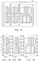
- FIGS. 11A, 11B and 11C are plan views of basic cells in the basic cell library of this invention and FIG. 12 is a plan view showing a chip on which the basic cells of FIGS. 11A, 11B and 11C are placed.
- the basic cells of this invention shown in the drawing are used for the layout of a standard cell type semiconductor device.
- FIG. 11A shows an A cell registered in the basic cell library.
- the basic cell has a dummy wiring pattern 4 of a polysilicon wiring pattern formed along a cell frame 1 which defines a cell region.
- the dummy wiring pattern 4 is formed of only portions 41 which are parallel to the polysilicon gate 3.
- the dummy wiring pattern 4 does not necessarily require portions which are perpendicular to the polysilicon gate 3.
- the dummy wiring pattern is formed in parallel to the internal wiring and has the same width as and substantially the same length as the internal wiring.
- one pair of diffusion regions 2 used as source/drain regions are formed.
- the diffusion regions include a p+ diffusion region 21 and n+ diffusion region 22 and one polysilicon gate 3 is formed to extend over the diffusion regions 21, 22.
- the gate width of the polysilicon gate 3 and the pattern width of the dummy wiring pattern 4 are both set to 0.3 ⁇ m, for example. Since the distance between the polysilicon gate 3 and the dummy wiring pattern 4 is constant, correction can be previously made in the state of basic cell if a variation in the gate width occurs in the polysilicon gate 3.
- FIG. 11B shows a B cell registered in the basic cell library, and two polysilicon gates 3 are each formed to extend over the p+ diffusion region 21 and n+ diffusion region 22.
- a dummy wiring pattern 4 of a polysilicon wiring pattern having the same width as the gate width of the polysilicon gate is formed to surround a cell region.
- the dummy wiring pattern 4 is formed of portions 41 which are parallel to the polysilicon gate 3.
- FIG. 11C shows a C cell registered in the basic cell library, and three polysilicon gates 3 are each formed to extend over the p+ diffusion region 21 and n+ diffusion region 22.
- a dummy wiring pattern 4 of a polysilicon wiring pattern having the same width as the gate width of the polysilicon gate is formed to surround a cell region.
- the dummy wiring pattern 4 is formed of portions 41 which are parallel to the polysilicon gate 3.
- basic cells are selected from the basic cell library and laid out on the chip.
- the design process is completed by laying out the basic cells such as the A cell, B cell, C cell shown in FIGS. 11A, 11B and 11C on the chip and then the chip forming process is started.
- the dummy wiring pattern of this invention can effectively cope with this compensation.
- FIG. 12 is a plan view showing a chip on which standard cells are laid out.
- basic cells A, B, C registered in the basic cell library are placed.
- the basic cells A to C are successively placed in a preset position in an order of ABC.
- a distance between the polysilicon gates varies depending on a difference in the layout of the basic cells on the chip, but the value correction of a mask for pattern formation for compensating for the optical proximity effect can be automatically made by effecting the layout process.
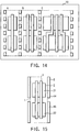
- FIGS. 13A, 13B, 13C and FIG. 14 are plan views showing basic cells in the basic cell library of this invention
- FIG. 14 is a plan view showing a chip on which the basic cells of FIGS. 13A, 13B and 13C are placed.
- the basic cells shown in the drawing are used for the layout of a standard cell type semiconductor device.
- FIG. 13A shows an A cell registered in the basic cell library.
- the basic cell has a dummy wiring pattern 4 of a polysilicon wiring pattern formed along a cell frame 1 which defines a cell region.
- the dummy wiring pattern 4 is formed of only portions 41 which are parallel to the polysilicon gate 3 and the parallel portion is constructed by a plurality of small portions 43 arranged on one row.
- the parallel portion 41 causes a variation in the gate width due to the optical proximity effect in the polysilicon gate 3
- the dummy wiring pattern 4 does not necessarily require portions which are perpendicular to the polysilicon gate 3.
- the structure in the cell region is the same as that in the basic cell (A cell) shown in FIG. 11A. Since the distance between the polysilicon gate 3 and the dummy wiring pattern 4 is constant, correction can be previously made in the state of basic cell if a variation in the gate width occurs in the polysilicon gate 3.
- FIG. 13B shows a B cell registered in the basic cell library, and the structure in the cell region is the same as that in the basic cell (B cell) of FIG. 11B.
- a dummy wiring pattern 4 of a polysilicon wiring pattern having the same width as the gate width of the polysilicon gate is formed to surround the cell region.
- the dummy wiring pattern 4 is formed of portions 41 which are parallel to the polysilicon gate 3 and the parallel portion is constructed by a plurality of small portions 43 placed on one row.
- FIG. 13C shows a C cell registered in the basic cell library, and the structure in the cell region is the same as that in the basic cell (C cell) of FIG. 11C.
- the dummy wiring pattern 4 is formed of portions 41 which are parallel to the polysilicon gate 3 and the parallel portion 41 is constructed by a plurality of small portions 43 placed on one row.
- the dummy wiring pattern is constructed by the small portions, it is possible to form the dummy wiring pattern according to a necessary covering rate.
- basic cells are selected from the basic cell library and laid out on the chip.
- the design process is completed by laying out the basic cells such as the A cell, B cell, C cell shown in FIGS. 13A, 13B and 13C on the chip and then the chip forming process is started.
- the dummy wiring pattern of this invention can effectively cope with this compensation.
- FIG. 14 is a plan view showing a chip on which standard cells are laid out.
- basic cells A, B, C registered in the basic cell library of FIGS. 13A, 13B and 13C are placed.
- the basic cells A to C are successively placed in a preset position in an order of ABC.
- a distance between the polysilicon gates varies depending on a difference in the layout of the basic cells on the chip, but the value correction of a mask for pattern formation for compensating for the optical proximity effect can be automatically made by effecting the layout process.
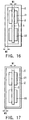
- FIGS. 15 to 17 are plan views showing basic cells in the basic cell library of this invention.
- the basic cells are used for the layout of a standard cell type semiconductor device.
- the basic cell of FIG. 15 has a dummy wiring pattern 4 of a polysilicon wiring pattern formed along a cell frame 1 which defines a cell region.
- the dummy wiring pattern 4 is formed of only portions which are parallel to the polysilicon gate 3 and the parallel portion is constructed by a plurality of small portions placed on one row.
- the dummy wiring pattern 4 does not necessarily require portions which are perpendicular to the polysilicon gate 3.
- One pair of diffusion regions 2 used as source/drain regions are formed in the cell region.
- the diffusion regions 2 include a p+ diffusion region 21 and an n+ diffusion region 22 and two polysilicon gates 3 are each formed to extend over the diffusion regions 21, 22.
- the gate width of the polysilicon gate 3 and the pattern width of the dummy wiring pattern 4 are both set to 0.3 ⁇ m, for example.
- the small portion has substantially the same size as the diffusion region. That is, the diffusion region 21 is formed to face a small portion 44 and the diffusion region 22 is formed to face a small portion 45.
- the distance between the polysilicon gate 3 and the dummy wiring pattern 4 is constant, correction can be previously made in the state of basic cell if a variation in the gate width occurs in the polysilicon gate 3. Further, since the dummy wiring pattern is divided, it is possible to form the dummy wiring pattern according to a necessary covering rate.
- the basic cell of FIG. 16 has a dummy wiring pattern 4 of a polysilicon wiring pattern formed along a cell frame which defines a cell region.
- the dummy wiring pattern 4 is formed to completely surround an element region in which the polysilicon gate 3 is formed.
- the pattern width w2 of the dummy wiring pattern 4 is made larger than the gate width w1 of the polysilicon gate 3 (w2 > w1).
- the basic cell of FIG. 17 has a dummy wiring pattern 4 of a polysilicon wiring pattern formed along a cell frame which defines a cell region.
- FIG. 17 has a dummy wiring pattern 4 of a polysilicon wiring pattern formed along a cell frame which defines a cell region. Like the case of FIG.
- the dummy wiring pattern 4 is formed to completely surround an element region in which the polysilicon gate 3 is formed.
- the pattern width w3 of the dummy wiring pattern 4 is made smaller than the gate width w1 of the polysilicon gate 3 (w3 ⁇ w1).
- the area of the basic cell formed on the chip can be reduced by setting the pattern width smaller than the gate width.
- this invention can be applied not only to the polysilicon wiring gate but also to a metal wiring of aluminum or another layer.
- FIG. 18 shows a sixth embodiment.
- a reference numeral 10 denotes a chip of an integrated circuit constructed by basic cells selectively taken out from the basic cell library of this invention.
- D, F, C in FIG. 18 denote basic cells, and since a dummy pattern is formed in each basic cell, it is not necessary to perform the OPC process for the whole portion of the chip and TAT can be reduced even if the integrated circuit is formed in a manner as shown in FIG. 18.
- the distance between a polysilicon gate used in a circuit and an adjacent dummy wiring pattern of a polysilicon wiring in the basic cell can be determined in the cell by previously forming means for compensating for the optical proximity effect in the cell frame of the basic cell registered in the basic cell library.
- a correction value by the OPC technique on the mask for correcting the gate width based on the variation in the poly-width can be determined only in the cell.
- the basic cell library is subjected to the correction by the OPC technique before cells of the product are arranged, it is not necessary to perform the OPC process at the time of development of the product, it is possible to prevent the delay in TAT caused by correction by the OPC technique for each product and an adequate mask of a polysilicon wiring pattern can be easily formed. Further, the amount of correction processing data can be made smaller than in the case of correction for the whole portion of the chip.
Landscapes
- Design And Manufacture Of Integrated Circuits (AREA)
- Preparing Plates And Mask In Photomechanical Process (AREA)
Applications Claiming Priority (3)
| Application Number | Priority Date | Filing Date | Title |
|---|---|---|---|
| JP20423696 | 1996-07-15 | ||
| JP20423696A JP3311244B2 (ja) | 1996-07-15 | 1996-07-15 | 基本セルライブラリ及びその形成方法 |
| JP204236/96 | 1996-07-15 |
Publications (2)
| Publication Number | Publication Date |
|---|---|
| EP0820100A2 true EP0820100A2 (de) | 1998-01-21 |
| EP0820100A3 EP0820100A3 (de) | 2001-05-16 |
Family
ID=16487110
Family Applications (1)
| Application Number | Title | Priority Date | Filing Date |
|---|---|---|---|
| EP97111750A Withdrawn EP0820100A3 (de) | 1996-07-15 | 1997-07-10 | Halbleiterbauteil und dessen Herstellungsverfahren, Grundzellenbibliothek und deren Herstellungsverfahren und Maske |
Country Status (5)
| Country | Link |
|---|---|
| US (2) | US5847421A (de) |
| EP (1) | EP0820100A3 (de) |
| JP (1) | JP3311244B2 (de) |
| KR (1) | KR100284104B1 (de) |
| TW (1) | TW434829B (de) |
Cited By (2)
| Publication number | Priority date | Publication date | Assignee | Title |
|---|---|---|---|---|
| WO2001043194A1 (en) * | 1999-12-10 | 2001-06-14 | Koninklijke Philips Electronics N.V. | Intelligent gate-level fill methods for reducing global pattern density effects |
| US7681166B2 (en) | 2007-09-28 | 2010-03-16 | Synopsys, Inc. | Method and apparatus for performing dummy-fill by using a set of dummy-fill cells |
Families Citing this family (119)
| Publication number | Priority date | Publication date | Assignee | Title |
|---|---|---|---|---|
| US6499003B2 (en) * | 1998-03-03 | 2002-12-24 | Lsi Logic Corporation | Method and apparatus for application of proximity correction with unitary segmentation |
| TW396398B (en) * | 1998-06-11 | 2000-07-01 | United Microelectronics Corp | Method for designing the assist feature to increase the process window |
| JP2000077609A (ja) * | 1998-08-28 | 2000-03-14 | Hitachi Ltd | 半導体集積回路装置 |
| KR100291384B1 (ko) * | 1998-12-31 | 2001-07-12 | 윤종용 | 반도체장치의레이아웃방법 |
| US6691297B1 (en) * | 1999-03-04 | 2004-02-10 | Matsushita Electric Industrial Co., Ltd. | Method for planning layout for LSI pattern, method for forming LSI pattern and method for generating mask data for LSI |
| US6238824B1 (en) | 1999-08-31 | 2001-05-29 | Micron Technology, Inc. | Method for designing and making photolithographic reticle, reticle, and photolithographic process |
| TW419723B (en) * | 1999-10-12 | 2001-01-21 | Vanguard Int Semiconduct Corp | Method of fabricating the capacitor array and its peripheral trench mask |
| US6426269B1 (en) | 1999-10-21 | 2002-07-30 | International Business Machines Corporation | Dummy feature reduction using optical proximity effect correction |
| KR100313280B1 (ko) * | 1999-10-25 | 2001-11-07 | 한신혁 | 반도체 장치의 전도배선 마스크 제조방법 |
| JP3912949B2 (ja) * | 1999-12-28 | 2007-05-09 | 株式会社東芝 | フォトマスクの形成方法及び半導体装置の製造方法 |
| TW486821B (en) * | 2000-01-10 | 2002-05-11 | Springsoft Inc | Method and system for constructing and manipulating a physical integrated circuit layout of a multiple-gate semiconductor device |
| US6316152B1 (en) | 2000-01-18 | 2001-11-13 | Taiwan Semiconductor Manufacturing Company | OPC method to improve e-beam writing time |
| US6737199B1 (en) | 2000-01-31 | 2004-05-18 | Taiwan Semiconductor Manufacturing Company | Using new pattern fracturing rules for optical proximity correction mask-making to improve critical dimension uniformity |
| JP2001230250A (ja) * | 2000-02-14 | 2001-08-24 | Hitachi Ltd | 半導体装置およびその製造方法並びにマスクパターンの生成方法 |
| JP4794030B2 (ja) * | 2000-07-10 | 2011-10-12 | ルネサスエレクトロニクス株式会社 | 半導体装置 |
| US6555895B1 (en) | 2000-07-17 | 2003-04-29 | General Semiconductor, Inc. | Devices and methods for addressing optical edge effects in connection with etched trenches |
| US6418551B1 (en) * | 2000-08-03 | 2002-07-09 | Avant! Corporation | Design rule checking tools and methods that use waiver layout patterns to waive unwanted dimensional check violations |
| US6794677B2 (en) * | 2000-10-02 | 2004-09-21 | Matsushita Electric Industrial Co., Ltd. | Semiconductor integrated circuit device and method for fabricating the same |
| JP2002229179A (ja) * | 2001-02-07 | 2002-08-14 | Nec Microsystems Ltd | 光近接効果補正方法 |
| KR100378195B1 (ko) | 2001-02-21 | 2003-03-29 | 삼성전자주식회사 | 패턴의 밀도에 연속적으로 조절되는 밀도를 갖는 더미패턴군들을 포함하는 마스크용 데이터 생성 방법 및그러한 생성 방법이 저장된 기록매체 |
| US6703641B2 (en) * | 2001-11-16 | 2004-03-09 | International Business Machines Corporation | Structure for detecting charging effects in device processing |
| US6734046B1 (en) * | 2001-11-28 | 2004-05-11 | Reshape, Inc. | Method of customizing and using maps in generating the padring layout design |
| US20040009409A1 (en) * | 2002-07-11 | 2004-01-15 | Jiunn-Ren Hwang | Optical proximity correction method |
| US6807663B2 (en) * | 2002-09-23 | 2004-10-19 | Numerical Technologies, Inc. | Accelerated layout processing using OPC pre-processing |
| JP4620942B2 (ja) * | 2003-08-21 | 2011-01-26 | 川崎マイクロエレクトロニクス株式会社 | 半導体集積回路のレイアウト方法、そのレイアウト構造、およびフォトマスク |
| JP3993545B2 (ja) | 2003-09-04 | 2007-10-17 | 株式会社東芝 | パターンの作製方法、半導体装置の製造方法、パターンの作製システム、セルライブラリ、フォトマスクの製造方法 |
| US7353492B2 (en) * | 2004-02-26 | 2008-04-01 | International Business Machines Corporation | Method of IC fabrication, IC mask fabrication and program product therefor |
| JP2005268610A (ja) * | 2004-03-19 | 2005-09-29 | Matsushita Electric Ind Co Ltd | スタンダードセルの設計方法及び半導体集積回路 |
| JP4248451B2 (ja) * | 2004-06-11 | 2009-04-02 | パナソニック株式会社 | 半導体装置およびそのレイアウト設計方法 |
| JP2006054430A (ja) * | 2004-07-12 | 2006-02-23 | Renesas Technology Corp | 半導体装置 |
| JP4175649B2 (ja) | 2004-07-22 | 2008-11-05 | 松下電器産業株式会社 | 半導体装置 |
| KR20060041547A (ko) * | 2004-11-09 | 2006-05-12 | 동부일렉트로닉스 주식회사 | Opc 마스크 제조 방법 |
| US7174532B2 (en) * | 2004-11-18 | 2007-02-06 | Agere Systems, Inc. | Method of making a semiconductor device by balancing shallow trench isolation stress and optical proximity effects |
| US9070623B2 (en) * | 2004-12-15 | 2015-06-30 | Taiwan Semiconductor Manufacturing Company, Ltd. | Controlling gate formation for high density cell layout |
| JP2007043049A (ja) * | 2004-12-20 | 2007-02-15 | Matsushita Electric Ind Co Ltd | セル、スタンダードセル、スタンダードセル配置方法、スタンダードセルライブラリ、ならびに半導体集積回路 |
| JP2006276079A (ja) * | 2005-03-28 | 2006-10-12 | National Institute Of Advanced Industrial & Technology | 光リソグラフィの光近接補正におけるマスクパターン設計方法および設計装置ならびにこれを用いた半導体装置の製造方法 |
| US7305643B2 (en) * | 2005-05-12 | 2007-12-04 | Freescale Semiconductor, Inc. | Method of tiling analog circuits that include resistors and capacitors |
| US7343581B2 (en) * | 2005-06-27 | 2008-03-11 | Tela Innovations, Inc. | Methods for creating primitive constructed standard cells |
| JP2007012855A (ja) | 2005-06-30 | 2007-01-18 | Matsushita Electric Ind Co Ltd | 半導体集積回路、標準セル、標準セルライブラリ、半導体集積回路の設計方法および半導体集積回路の設計装置 |
| US7244975B2 (en) * | 2005-07-05 | 2007-07-17 | United Microelectronics Corp. | High-voltage device structure |
| WO2007038972A1 (en) * | 2005-09-20 | 2007-04-12 | Freescale Semiconductor, Inc. | Method of making an integrated circuit |
| KR100712996B1 (ko) * | 2005-09-20 | 2007-05-02 | 주식회사 하이닉스반도체 | 패턴더미를 갖는 반도체소자 및 패턴더미를 이용한반도체소자의 제조방법 |
| JP4796817B2 (ja) * | 2005-10-31 | 2011-10-19 | エルピーダメモリ株式会社 | 基本セル設計方法、レイアウト設計方法、設計装置およびプログラム |
| JP4575274B2 (ja) * | 2005-10-31 | 2010-11-04 | 富士通セミコンダクター株式会社 | パターンレイアウト、レイアウトデータの生成方法及び半導体装置 |
| JP2007129026A (ja) * | 2005-11-02 | 2007-05-24 | Nec Electronics Corp | 半導体装置および配線パターン形成方法、マスク配線データ発生方法 |
| US7934184B2 (en) * | 2005-11-14 | 2011-04-26 | Takumi Technology Corporation | Integrated circuit design using modified cells |
| US7590968B1 (en) | 2006-03-01 | 2009-09-15 | Tela Innovations, Inc. | Methods for risk-informed chip layout generation |
| US7446352B2 (en) | 2006-03-09 | 2008-11-04 | Tela Innovations, Inc. | Dynamic array architecture |
| US8448102B2 (en) | 2006-03-09 | 2013-05-21 | Tela Innovations, Inc. | Optimizing layout of irregular structures in regular layout context |
| US8653857B2 (en) | 2006-03-09 | 2014-02-18 | Tela Innovations, Inc. | Circuitry and layouts for XOR and XNOR logic |
| US7932545B2 (en) | 2006-03-09 | 2011-04-26 | Tela Innovations, Inc. | Semiconductor device and associated layouts including gate electrode level region having arrangement of six linear conductive segments with side-to-side spacing less than 360 nanometers |
| US7943967B2 (en) | 2006-03-09 | 2011-05-17 | Tela Innovations, Inc. | Semiconductor device and associated layouts including diffusion contact placement restriction based on relation to linear conductive segments |
| US8225261B2 (en) | 2006-03-09 | 2012-07-17 | Tela Innovations, Inc. | Methods for defining contact grid in dynamic array architecture |
| US8245180B2 (en) | 2006-03-09 | 2012-08-14 | Tela Innovations, Inc. | Methods for defining and using co-optimized nanopatterns for integrated circuit design and apparatus implementing same |
| US7763534B2 (en) | 2007-10-26 | 2010-07-27 | Tela Innovations, Inc. | Methods, structures and designs for self-aligning local interconnects used in integrated circuits |
| US8541879B2 (en) | 2007-12-13 | 2013-09-24 | Tela Innovations, Inc. | Super-self-aligned contacts and method for making the same |
| US9563733B2 (en) | 2009-05-06 | 2017-02-07 | Tela Innovations, Inc. | Cell circuit and layout with linear finfet structures |
| US9230910B2 (en) | 2006-03-09 | 2016-01-05 | Tela Innovations, Inc. | Oversized contacts and vias in layout defined by linearly constrained topology |
| US9035359B2 (en) | 2006-03-09 | 2015-05-19 | Tela Innovations, Inc. | Semiconductor chip including region including linear-shaped conductive structures forming gate electrodes and having electrical connection areas arranged relative to inner region between transistors of different types and associated methods |
| US9009641B2 (en) | 2006-03-09 | 2015-04-14 | Tela Innovations, Inc. | Circuits with linear finfet structures |
| US7956421B2 (en) | 2008-03-13 | 2011-06-07 | Tela Innovations, Inc. | Cross-coupled transistor layouts in restricted gate level layout architecture |
| US8658542B2 (en) | 2006-03-09 | 2014-02-25 | Tela Innovations, Inc. | Coarse grid design methods and structures |
| US7908578B2 (en) * | 2007-08-02 | 2011-03-15 | Tela Innovations, Inc. | Methods for designing semiconductor device with dynamic array section |
| US8839175B2 (en) | 2006-03-09 | 2014-09-16 | Tela Innovations, Inc. | Scalable meta-data objects |
| US8225239B2 (en) | 2006-03-09 | 2012-07-17 | Tela Innovations, Inc. | Methods for defining and utilizing sub-resolution features in linear topology |
| US8247846B2 (en) | 2006-03-09 | 2012-08-21 | Tela Innovations, Inc. | Oversized contacts and vias in semiconductor chip defined by linearly constrained topology |
| JP4476232B2 (ja) * | 2006-03-10 | 2010-06-09 | 三菱重工業株式会社 | 成膜装置のシーズニング方法 |
| JP2008020751A (ja) * | 2006-07-13 | 2008-01-31 | National Institute Of Advanced Industrial & Technology | マスクパターン設計方法およびそれを用いた半導体装置の製造方法 |
| US7577049B1 (en) | 2006-08-08 | 2009-08-18 | Tela Innovations, Inc. | Speculative sense enable tuning apparatus and associated methods |
| WO2008023660A1 (en) * | 2006-08-25 | 2008-02-28 | National Institute Of Advanced Industrial Science And Technology | Mask pattern designing method and semiconductor device manufacturing method using the same |
| JP4714854B2 (ja) * | 2006-09-05 | 2011-06-29 | 独立行政法人産業技術総合研究所 | マスクパターン設計方法、マスクパターン設計装置および半導体装置の製造方法 |
| JP4851924B2 (ja) * | 2006-12-08 | 2012-01-11 | 株式会社東芝 | 危険箇所集計方法、パターン修正方法およびプログラム |
| JP4883591B2 (ja) * | 2007-01-26 | 2012-02-22 | 独立行政法人産業技術総合研究所 | マスクパターン設計方法および半導体装置の製造方法 |
| US7765515B2 (en) * | 2007-02-03 | 2010-07-27 | Anchor Semiconductor, Inc. | Pattern match based optical proximity correction and verification of integrated circuit layout |
| US8286107B2 (en) | 2007-02-20 | 2012-10-09 | Tela Innovations, Inc. | Methods and systems for process compensation technique acceleration |
| US7979829B2 (en) * | 2007-02-20 | 2011-07-12 | Tela Innovations, Inc. | Integrated circuit cell library with cell-level process compensation technique (PCT) application and associated methods |
| US8667443B2 (en) | 2007-03-05 | 2014-03-04 | Tela Innovations, Inc. | Integrated circuit cell library for multiple patterning |
| JP2008235350A (ja) * | 2007-03-16 | 2008-10-02 | Matsushita Electric Ind Co Ltd | 半導体集積回路 |
| US7763398B2 (en) * | 2007-05-02 | 2010-07-27 | Dongbu Hitek Co., Ltd. | Layout method for mask |
| JP2008311361A (ja) | 2007-06-13 | 2008-12-25 | Nec Electronics Corp | 半導体集積回路、半導体集積回路のレイアウト設計方法、及び半導体集積回路の自動レイアウトプログラム |
| US8453094B2 (en) | 2008-01-31 | 2013-05-28 | Tela Innovations, Inc. | Enforcement of semiconductor structure regularity for localized transistors and interconnect |
| US7939443B2 (en) | 2008-03-27 | 2011-05-10 | Tela Innovations, Inc. | Methods for multi-wire routing and apparatus implementing same |
| JP5415710B2 (ja) * | 2008-04-10 | 2014-02-12 | ルネサスエレクトロニクス株式会社 | 半導体装置 |
| US20090261419A1 (en) * | 2008-04-22 | 2009-10-22 | Shu-Ping Fang | Semiconductor device having assist features and manufacturing method thereof |
| US8004014B2 (en) | 2008-07-04 | 2011-08-23 | Panasonic Corporation | Semiconductor integrated circuit device having metal interconnect regions placed symmetrically with respect to a cell boundary |
| JP2010016258A (ja) * | 2008-07-04 | 2010-01-21 | Panasonic Corp | 半導体集積回路装置 |
| JP5292005B2 (ja) * | 2008-07-14 | 2013-09-18 | ルネサスエレクトロニクス株式会社 | 半導体集積回路 |
| KR101761530B1 (ko) | 2008-07-16 | 2017-07-25 | 텔라 이노베이션스, 인코포레이티드 | 동적 어레이 아키텍쳐에서의 셀 페이징과 배치를 위한 방법 및 그 구현 |
| US9122832B2 (en) | 2008-08-01 | 2015-09-01 | Tela Innovations, Inc. | Methods for controlling microloading variation in semiconductor wafer layout and fabrication |
| CN101930966B (zh) * | 2009-06-24 | 2014-07-02 | 联华电子股份有限公司 | 电路布局结构及缩小集成电路布局的方法 |
| US8661392B2 (en) | 2009-10-13 | 2014-02-25 | Tela Innovations, Inc. | Methods for cell boundary encroachment and layouts implementing the Same |
| JP5331195B2 (ja) | 2009-10-19 | 2013-10-30 | パナソニック株式会社 | 半導体装置 |
| US9646958B2 (en) * | 2010-03-17 | 2017-05-09 | Taiwan Semiconductor Manufacturing Company, Ltd. | Integrated circuits including dummy structures and methods of forming the same |
| JP5427104B2 (ja) * | 2010-05-11 | 2014-02-26 | パナソニック株式会社 | パターン形成方法 |
| US9159627B2 (en) | 2010-11-12 | 2015-10-13 | Tela Innovations, Inc. | Methods for linewidth modification and apparatus implementing the same |
| JP5603768B2 (ja) * | 2010-12-28 | 2014-10-08 | 株式会社東芝 | 半導体集積回路の配線方法、半導体回路配線装置および半導体集積回路 |
| JP2013003162A (ja) | 2011-06-10 | 2013-01-07 | Renesas Electronics Corp | マスクデータ検証装置、設計レイアウト検証装置、それらの方法およびそれらのコンピュータ・プログラム |
| US8643069B2 (en) | 2011-07-12 | 2014-02-04 | United Microelectronics Corp. | Semiconductor device having metal gate and manufacturing method thereof |
| JP5554303B2 (ja) | 2011-09-08 | 2014-07-23 | 株式会社東芝 | 半導体集積回路および半導体集積回路の設計方法 |
| US8673755B2 (en) | 2011-10-27 | 2014-03-18 | United Microelectronics Corp. | Semiconductor device having metal gate and manufacturing method thereof |
| WO2013121485A1 (ja) | 2012-02-13 | 2013-08-22 | パナソニック株式会社 | フォトマスク及びそれを用いたパターン形成方法 |
| JP5935475B2 (ja) * | 2012-04-18 | 2016-06-15 | 株式会社ソシオネクスト | セルライブラリおよびパターンデータ生成方法 |
| CN102664142B (zh) * | 2012-04-19 | 2014-10-22 | 浙江大学 | 对现有版图填充冗余多晶硅条阵列的插入方法 |
| US9136170B2 (en) | 2012-05-30 | 2015-09-15 | United Microelectronics Corp. | Through silicon via (TSV) structure and process thereof |
| USD729808S1 (en) * | 2013-03-13 | 2015-05-19 | Nagrastar Llc | Smart card interface |
| US8836129B1 (en) | 2013-03-14 | 2014-09-16 | United Microelectronics Corp. | Plug structure |
| US9438237B1 (en) * | 2013-04-19 | 2016-09-06 | Pdf Solutions, Inc. | High-yielding standard cell library and circuits made therefrom |
| US8759885B1 (en) * | 2013-04-30 | 2014-06-24 | Freescale Semiconductor, Inc. | Standard cell for semiconductor device |
| US9009633B2 (en) * | 2013-05-06 | 2015-04-14 | United Microelectronics Corp. | Method of correcting assist feature |
| JP6418786B2 (ja) * | 2013-07-10 | 2018-11-07 | キヤノン株式会社 | パターンの作成方法、プログラムおよび情報処理装置 |
| US9710588B2 (en) * | 2014-08-05 | 2017-07-18 | Taiwan Semiconductor Manufacturing Company, Ltd. | Method of generating modified layout for RC extraction |
| USD780763S1 (en) * | 2015-03-20 | 2017-03-07 | Nagrastar Llc | Smart card interface |
| USD776664S1 (en) * | 2015-05-20 | 2017-01-17 | Chaya Coleena Hendrick | Smart card |
| US10789407B1 (en) * | 2016-03-30 | 2020-09-29 | Silicon Technologies, Inc. | Analog design tool having a cell set, and related methods |
| US9641161B1 (en) | 2016-05-02 | 2017-05-02 | Taiwan Semiconductor Manufacturing Co., Ltd. | Flip-flop with delineated layout for reduced footprint |
| CN111106112B (zh) * | 2018-10-25 | 2025-01-10 | 长鑫存储技术有限公司 | 半导体器件结构及其制备方法 |
| US10930675B2 (en) * | 2018-11-20 | 2021-02-23 | Samsung Electronics Co., Ltd. | Semiconductor device |
| KR102818902B1 (ko) * | 2021-02-05 | 2025-06-12 | 창신 메모리 테크놀로지즈 아이엔씨 | 표준 셀 레이아웃 템플릿 및 반도체 구조물 |
| EP4086957A4 (de) * | 2021-03-17 | 2023-06-14 | Changxin Memory Technologies, Inc. | Integrierte schaltung und layoutverfahren dafür |
Family Cites Families (14)
| Publication number | Priority date | Publication date | Assignee | Title |
|---|---|---|---|---|
| US4520269A (en) * | 1982-11-03 | 1985-05-28 | International Business Machines Corporation | Electron beam lithography proximity correction method |
| JPH0828467B2 (ja) * | 1988-11-15 | 1996-03-21 | 株式会社東芝 | 半導体装置 |
| JPH03171735A (ja) * | 1989-11-30 | 1991-07-25 | Matsushita Electron Corp | 半導体装置の製造方法 |
| DE69128819T2 (de) * | 1990-08-13 | 1998-05-14 | Nippon Electric Co | Halbleiterspeicheranordnung |
| JP3132582B2 (ja) * | 1991-07-12 | 2001-02-05 | 日本電気株式会社 | 半導体装置 |
| US5278105A (en) * | 1992-08-19 | 1994-01-11 | Intel Corporation | Semiconductor device with dummy features in active layers |
| US5441915A (en) * | 1992-09-01 | 1995-08-15 | Taiwan Semiconductor Manufacturing Company Ltd. | Process of fabrication planarized metallurgy structure for a semiconductor device |
| JPH077064A (ja) * | 1993-06-16 | 1995-01-10 | Hiroshima Nippon Denki Kk | 半導体集積回路 |
| KR100194130B1 (ko) * | 1994-03-30 | 1999-06-15 | 니시무로 타이죠 | 반도체 패키지 |
| US5682323A (en) * | 1995-03-06 | 1997-10-28 | Lsi Logic Corporation | System and method for performing optical proximity correction on macrocell libraries |
| US5553273A (en) * | 1995-04-17 | 1996-09-03 | International Business Machines Corporation | Vertex minimization in a smart optical proximity correction system |
| US5663017A (en) * | 1995-06-07 | 1997-09-02 | Lsi Logic Corporation | Optical corrective techniques with reticle formation and reticle stitching to provide design flexibility |
| US5705301A (en) * | 1996-02-27 | 1998-01-06 | Lsi Logic Corporation | Performing optical proximity correction with the aid of design rule checkers |
| US5723233A (en) * | 1996-02-27 | 1998-03-03 | Lsi Logic Corporation | Optical proximity correction method and apparatus |
-
1996
- 1996-07-15 JP JP20423696A patent/JP3311244B2/ja not_active Expired - Fee Related
-
1997
- 1997-06-28 TW TW086109113A patent/TW434829B/zh not_active IP Right Cessation
- 1997-07-10 EP EP97111750A patent/EP0820100A3/de not_active Withdrawn
- 1997-07-11 KR KR1019970032167A patent/KR100284104B1/ko not_active Expired - Fee Related
- 1997-07-14 US US08/891,842 patent/US5847421A/en not_active Expired - Fee Related
-
1998
- 1998-10-07 US US09/167,536 patent/US6194252B1/en not_active Expired - Fee Related
Cited By (5)
| Publication number | Priority date | Publication date | Assignee | Title |
|---|---|---|---|---|
| WO2001043194A1 (en) * | 1999-12-10 | 2001-06-14 | Koninklijke Philips Electronics N.V. | Intelligent gate-level fill methods for reducing global pattern density effects |
| US6323113B1 (en) | 1999-12-10 | 2001-11-27 | Philips Electronics North America Corporation | Intelligent gate-level fill methods for reducing global pattern density effects |
| KR100750409B1 (ko) * | 1999-12-10 | 2007-08-21 | 코닌클리즈케 필립스 일렉트로닉스 엔.브이. | 게이트 층을 더미 충진 패턴으로 충진하는 방법 및 게이트 층 내의 더미 충진 위치를 식별하는 자동화된 방법 |
| US7681166B2 (en) | 2007-09-28 | 2010-03-16 | Synopsys, Inc. | Method and apparatus for performing dummy-fill by using a set of dummy-fill cells |
| CN101689214B (zh) * | 2007-09-28 | 2012-11-28 | 新思科技有限公司 | 通过使用一组哑元填充单元来执行哑元填充的方法和设备 |
Also Published As
| Publication number | Publication date |
|---|---|
| US6194252B1 (en) | 2001-02-27 |
| EP0820100A3 (de) | 2001-05-16 |
| US5847421A (en) | 1998-12-08 |
| TW434829B (en) | 2001-05-16 |
| JP3311244B2 (ja) | 2002-08-05 |
| KR100284104B1 (ko) | 2001-04-02 |
| JPH1032253A (ja) | 1998-02-03 |
Similar Documents
| Publication | Publication Date | Title |
|---|---|---|
| US5847421A (en) | Logic cell having efficient optical proximity effect correction | |
| CN102610606B (zh) | 半导体装置及其制造方法、光接近处理方法 | |
| US7404165B2 (en) | Method for planning layout for LSI pattern, method for forming LSI pattern and method for generating mask data for LSI | |
| US20050193363A1 (en) | Method of IC fabrication, IC mask fabrication and program product therefor | |
| EP0182222B1 (de) | Integrierte Halbleiterschaltungsanordnung in Polycell-Technik | |
| CN121386285B (zh) | 掩膜图案的生成方法、掩膜、半导体结构及其制造方法 | |
| JP2002055431A (ja) | マスクデータパターン生成方法 | |
| US6519758B2 (en) | Method of checking exposure patterns formed over photo-mask | |
| US8143724B2 (en) | Standard cell and semiconductor device including the same | |
| US7320904B2 (en) | Manufacturing method for non-active electrically structures in order to optimize the definition of active electrically structures in an electronic circuit integrated on a semiconductor substrate and corresponding circuit | |
| JP2004288685A (ja) | 半導体集積回路のレイアウト設計方法およびレイアウト設計用プログラム | |
| US6780745B2 (en) | Semiconductor integrated circuit and method of manufacturing the same | |
| US7315054B1 (en) | Decoupling capacitor density while maintaining control over ACLV regions on a semiconductor integrated circuit | |
| EP0414412A2 (de) | Integrierte Halbleiterschaltungsanordnung mit Leiterschichten | |
| JP2887972B2 (ja) | 半導体集積回路装置の製造方法 | |
| KR100761393B1 (ko) | 플래시소자의 소자분리를 위한 갭필테스트패턴의 형성 방법 | |
| KR19980018507A (ko) | 반도체 장치 | |
| JPS60249347A (ja) | セミカスタムicの製造方法 | |
| JP2002365812A (ja) | 半導体装置の製造方法 | |
| JPH09172073A (ja) | 半導体集積回路の自動配置配線方法 |
Legal Events
| Date | Code | Title | Description |
|---|---|---|---|
| PUAI | Public reference made under article 153(3) epc to a published international application that has entered the european phase |
Free format text: ORIGINAL CODE: 0009012 |
|
| 17P | Request for examination filed |
Effective date: 19970710 |
|
| AK | Designated contracting states |
Kind code of ref document: A2 Designated state(s): DE FR GB |
|
| AX | Request for extension of the european patent |
Free format text: AL;LT;LV;RO;SI |
|
| PUAL | Search report despatched |
Free format text: ORIGINAL CODE: 0009013 |
|
| AK | Designated contracting states |
Kind code of ref document: A3 Designated state(s): AT BE CH DE DK ES FI FR GB GR IE IT LI LU MC NL PT SE |
|
| AX | Request for extension of the european patent |
Free format text: AL;LT;LV;RO;SI |
|
| AKX | Designation fees paid |
Free format text: DE FR GB |
|
| 17Q | First examination report despatched |
Effective date: 20020604 |
|
| 17Q | First examination report despatched |
Effective date: 20020604 |
|
| STAA | Information on the status of an ep patent application or granted ep patent |
Free format text: STATUS: THE APPLICATION IS DEEMED TO BE WITHDRAWN |
|
| 18D | Application deemed to be withdrawn |
Effective date: 20090422 |