EP0821338A2 - Adressgenerator für Anzeige und Lichtmodulator mit rekonfigurierbarem Schieberegister - Google Patents
Adressgenerator für Anzeige und Lichtmodulator mit rekonfigurierbarem Schieberegister Download PDFInfo
- Publication number
- EP0821338A2 EP0821338A2 EP97304638A EP97304638A EP0821338A2 EP 0821338 A2 EP0821338 A2 EP 0821338A2 EP 97304638 A EP97304638 A EP 97304638A EP 97304638 A EP97304638 A EP 97304638A EP 0821338 A2 EP0821338 A2 EP 0821338A2
- Authority
- EP
- European Patent Office
- Prior art keywords
- shift register
- display
- generator
- stages
- stage
- Prior art date
- Legal status (The legal status is an assumption and is not a legal conclusion. Google has not performed a legal analysis and makes no representation as to the accuracy of the status listed.)
- Granted
Links
- 239000011159 matrix material Substances 0.000 claims abstract description 14
- 230000015654 memory Effects 0.000 claims description 29
- 239000004973 liquid crystal related substance Substances 0.000 claims description 6
- 238000010586 diagram Methods 0.000 description 7
- 238000005516 engineering process Methods 0.000 description 6
- 230000006870 function Effects 0.000 description 6
- 238000000034 method Methods 0.000 description 4
- 230000003287 optical effect Effects 0.000 description 4
- 230000001427 coherent effect Effects 0.000 description 3
- 230000000007 visual effect Effects 0.000 description 3
- XUIMIQQOPSSXEZ-UHFFFAOYSA-N Silicon Chemical compound [Si] XUIMIQQOPSSXEZ-UHFFFAOYSA-N 0.000 description 2
- 230000004075 alteration Effects 0.000 description 2
- 230000008901 benefit Effects 0.000 description 2
- 239000000835 fiber Substances 0.000 description 2
- 230000005669 field effect Effects 0.000 description 2
- 229910044991 metal oxide Inorganic materials 0.000 description 2
- 150000004706 metal oxides Chemical class 0.000 description 2
- 230000004048 modification Effects 0.000 description 2
- 238000012986 modification Methods 0.000 description 2
- 230000008569 process Effects 0.000 description 2
- 230000003134 recirculating effect Effects 0.000 description 2
- 230000009467 reduction Effects 0.000 description 2
- 229910052710 silicon Inorganic materials 0.000 description 2
- 239000010703 silicon Substances 0.000 description 2
- 208000036693 Color-vision disease Diseases 0.000 description 1
- 229910021417 amorphous silicon Inorganic materials 0.000 description 1
- 238000004458 analytical method Methods 0.000 description 1
- 238000004364 calculation method Methods 0.000 description 1
- 201000007254 color blindness Diseases 0.000 description 1
- 239000003086 colorant Substances 0.000 description 1
- 230000000295 complement effect Effects 0.000 description 1
- 238000013500 data storage Methods 0.000 description 1
- 230000001934 delay Effects 0.000 description 1
- 230000001419 dependent effect Effects 0.000 description 1
- 238000005265 energy consumption Methods 0.000 description 1
- 230000014509 gene expression Effects 0.000 description 1
- 239000011521 glass Substances 0.000 description 1
- 238000007648 laser printing Methods 0.000 description 1
- 230000003071 parasitic effect Effects 0.000 description 1
- 230000005043 peripheral vision Effects 0.000 description 1
- 229910021420 polycrystalline silicon Inorganic materials 0.000 description 1
- 229920005591 polysilicon Polymers 0.000 description 1
- 210000001747 pupil Anatomy 0.000 description 1
- 230000010076 replication Effects 0.000 description 1
- 230000004044 response Effects 0.000 description 1
- 230000002207 retinal effect Effects 0.000 description 1
- 239000004065 semiconductor Substances 0.000 description 1
- 239000007787 solid Substances 0.000 description 1
- 239000000758 substrate Substances 0.000 description 1
- 230000001360 synchronised effect Effects 0.000 description 1
Images



Classifications
-
- G—PHYSICS
- G09—EDUCATION; CRYPTOGRAPHY; DISPLAY; ADVERTISING; SEALS
- G09G—ARRANGEMENTS OR CIRCUITS FOR CONTROL OF INDICATING DEVICES USING STATIC MEANS TO PRESENT VARIABLE INFORMATION
- G09G3/00—Control arrangements or circuits, of interest only in connection with visual indicators other than cathode-ray tubes
- G09G3/20—Control arrangements or circuits, of interest only in connection with visual indicators other than cathode-ray tubes for presentation of an assembly of a number of characters, e.g. a page, by composing the assembly by combination of individual elements arranged in a matrix no fixed position being assigned to or needed to be assigned to the individual characters or partial characters
- G09G3/34—Control arrangements or circuits, of interest only in connection with visual indicators other than cathode-ray tubes for presentation of an assembly of a number of characters, e.g. a page, by composing the assembly by combination of individual elements arranged in a matrix no fixed position being assigned to or needed to be assigned to the individual characters or partial characters by control of light from an independent source
- G09G3/36—Control arrangements or circuits, of interest only in connection with visual indicators other than cathode-ray tubes for presentation of an assembly of a number of characters, e.g. a page, by composing the assembly by combination of individual elements arranged in a matrix no fixed position being assigned to or needed to be assigned to the individual characters or partial characters by control of light from an independent source using liquid crystals
- G09G3/3611—Control of matrices with row and column drivers
- G09G3/3674—Details of drivers for scan electrodes
-
- G—PHYSICS
- G09—EDUCATION; CRYPTOGRAPHY; DISPLAY; ADVERTISING; SEALS
- G09G—ARRANGEMENTS OR CIRCUITS FOR CONTROL OF INDICATING DEVICES USING STATIC MEANS TO PRESENT VARIABLE INFORMATION
- G09G3/00—Control arrangements or circuits, of interest only in connection with visual indicators other than cathode-ray tubes
- G09G3/20—Control arrangements or circuits, of interest only in connection with visual indicators other than cathode-ray tubes for presentation of an assembly of a number of characters, e.g. a page, by composing the assembly by combination of individual elements arranged in a matrix no fixed position being assigned to or needed to be assigned to the individual characters or partial characters
- G09G3/34—Control arrangements or circuits, of interest only in connection with visual indicators other than cathode-ray tubes for presentation of an assembly of a number of characters, e.g. a page, by composing the assembly by combination of individual elements arranged in a matrix no fixed position being assigned to or needed to be assigned to the individual characters or partial characters by control of light from an independent source
- G09G3/36—Control arrangements or circuits, of interest only in connection with visual indicators other than cathode-ray tubes for presentation of an assembly of a number of characters, e.g. a page, by composing the assembly by combination of individual elements arranged in a matrix no fixed position being assigned to or needed to be assigned to the individual characters or partial characters by control of light from an independent source using liquid crystals
- G09G3/3611—Control of matrices with row and column drivers
- G09G3/3685—Details of drivers for data electrodes
-
- G—PHYSICS
- G09—EDUCATION; CRYPTOGRAPHY; DISPLAY; ADVERTISING; SEALS
- G09G—ARRANGEMENTS OR CIRCUITS FOR CONTROL OF INDICATING DEVICES USING STATIC MEANS TO PRESENT VARIABLE INFORMATION
- G09G2310/00—Command of the display device
- G09G2310/02—Addressing, scanning or driving the display screen or processing steps related thereto
- G09G2310/0202—Addressing of scan or signal lines
- G09G2310/0205—Simultaneous scanning of several lines in flat panels
-
- G—PHYSICS
- G09—EDUCATION; CRYPTOGRAPHY; DISPLAY; ADVERTISING; SEALS
- G09G—ARRANGEMENTS OR CIRCUITS FOR CONTROL OF INDICATING DEVICES USING STATIC MEANS TO PRESENT VARIABLE INFORMATION
- G09G2310/00—Command of the display device
- G09G2310/02—Addressing, scanning or driving the display screen or processing steps related thereto
- G09G2310/0235—Field-sequential colour display
-
- G—PHYSICS
- G09—EDUCATION; CRYPTOGRAPHY; DISPLAY; ADVERTISING; SEALS
- G09G—ARRANGEMENTS OR CIRCUITS FOR CONTROL OF INDICATING DEVICES USING STATIC MEANS TO PRESENT VARIABLE INFORMATION
- G09G2340/00—Aspects of display data processing
- G09G2340/04—Changes in size, position or resolution of an image
- G09G2340/0407—Resolution change, inclusive of the use of different resolutions for different screen areas
Definitions
- the present invention relates to an address generator for a display or spatial light modulator.
- the invention also relates to a display and to a spatial light modulator.
- an address generator for a display or spatial light modulator comprising a first shift register having a plurality of cascade-connected stages for controlling respective first address electrodes of the display or spatial light modulator, characterised in that the stages of the first shift register include a first reconfigurable shift register stage which is selectively operable in an alternate mode, in which the output of the first reconfigurable shift register stage follows the output of a preceding stage.
- the first shift register may be an analogue shift register.
- the first shift register may be a digital shift register.
- Each stage of the first shift register may comprise a first memory having a first memory enable input connected to a first phase of a first bi-phase clock line and a second memory having a second memory enable input connected to a second phase of the first bi-phase clock line, the first memory enable input of the first reconfigurable shift register stage of the first shift register being selectively connectable to the second phase of the first bi-phase clock line.
- Each of the first and second memories may comprise a bistable circuit.
- Each of the stages subsequent to a first stage of the first shift register may comprise a switch for selectively connecting the first memory enable input to the first or second phase of the first bi-phase clock line.
- the generator may comprise a first further shift register having a plurality of cascade-connected stages for controlling respective ones of the switches of the first shift register.
- the first shift register may comprise a first sub-shift register having a first plurality of cascade-connected sub-stages and a second sub-shift register having a second plurality of cascade-connected sub-stages, the first plurality of sub-stages being interlaced with the second plurality of sub-stages.
- the generator may comprise a second shift register having a plurality of cascade-connected stages for controlling respective second address electrodes of the display or spatial light modulator, the stages of the second shift register including a second reconfigurable shift register stage which is selectively operable in the alternate mode.
- the second shift register may be an analogue shift register.
- the second shift register may be a digital shift register.
- Each stage of the second shift register may comprise a third memory having a third memory enable input connected to a first phase of a second bi-phase clock line and a fourth memory having a fourth memory enable input connected to a second phase of the second bi-phase clock line, the third memory enable input of the second reconfigurable shift register stage of the second shift register being selectively connectable to the second phase of the second bi-phase clock line.
- Each of the third and fourth memories may comprise a bi-stable circuit.
- Each of the stages of the second shift register subsequent to a first stage thereof may comprise a switch for selectively connecting the third memory enable input to the first or second phase of the second bi-phase clock line.
- the generator may comprise a second further shift register having a plurality of cascade-connected stages for controlling respective ones of the switches of the second shift register.
- a spatial light modulator including an address generator in accordance with the first aspect of the invention.
- the spatial light modulator may be of the matrix type, for instance of the active matrix type, and may be of liquid crystal type.
- a display including an address generator according to the first aspect of the invention.
- the display may be of matrix type, for instance of active matrix type, and may be of liquid crystal type.
- a display characterised by a display device, a tracking for determining an observed region of the display device at which an observer is looking, and an image data generator responsive to the tracker for generating image data with a first spatial resolution for the observed region and with a second spatial resolution less than the first resolution for another region of the display device.
- the display device may comprise a display according to the third aspect of the invention.
- the device may be operated at reduced resolution. This allows the addressing speed of the device to be increased while reducing the amount of data required to update each frame.
- the device itself does not require modification to achieve this.
- the address generator or generators supply signals which allow variable resolution to be achieved without modification of the basic device.
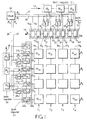
- the device shown in Figure 1 may be embodied as a spatial light modulator or as a display using any suitable addressing and optical or light emitting technology. However, for convenience of description, the device of Figure 1 will be described as an active matrix liquid crystal display.
- the display comprises n rows R 1 to R n and m columns C 1 to C m arranged as a rectangular matrix of picture elements (pixels) 10 11 to 10 mn , where the pixel of the ith column and the jth row is referred to as 10 ij .
- pixels picture elements
- the columns of the display are addressed by means of column electrodes 11 1 to 11 m which are connected to a shift register 12.
- the shift register 12 comprises cascade-connected stages 13 1 to 13 m to form a series-in/parallel-out shift register having a data input 14 for receiving serial display row data.
- Each of the shift register stages 13 1 to 13 m comprises first and second memory devices 15 11 , 15 12 , to 15 m1 , 15 m2 .
- Each of the second memory devices 15 12 to 15 m2 has an output connected to the respective column addressing line 11 1 to 11 m and to the input of the first memory device of the succeeding shift register stage.
- the second memory devices 15 12 to 15 m2 have clock inputs connected to a second line 17 of a bi-phase clock line which receives clock signals ⁇ 2 from a clock 18.
- the first memory device 15 11 of the first stage 13 1 has a clock input connected to a first line 16 of the bi-phase clock line and receives clock signals ⁇ 1 from the clock 18.
- the first memory devices 15 21 to 15 m1 of the remaining stages 13 2 to 13 m of the shift register 12 are connected to respective switching elements 19 2 to 19 m , each of which has first and second inputs connected to the lines 16 and 17, respectively.
- the switching elements 19 2 to 19 m have switch control inputs connected to the outputs of respective stages 20 2 to 20 m of a shift register 21 of the serial-in/parallel-out type.
- the shift register 21 has an input 22 for receiving configuration data in serial form for determining which of the first and second inputs of each switching element 19 2 to 19 m is connected to its output. Suitable arrangements (not shown) are providing for clocking the configuration data into the shift register 21.
- the display further comprises row addressing electrodes 22 1 to 22 n which are connected to the outputs of respective stages 23 1 to 23 n of a shift register 24.
- the stages of the shift register 24 comprise first and second memory devices 25 11 , 25 12 to 25 n1 , 25 n2 .
- the shift register 24 is of the same type as the shift register 12 and differs therefrom only in that the input of the first memory device 25 11 is connected to the output of the last memory device 25 n2 so that the shift register 24 operates as a "ring register” continually recirculating the binary data therein.
- Means (not shown) are provided for presetting the shift register 24 when power is applied to the display such that the memory device 25 12 is set to "1" whereas all of the other memory devices are reset to "zero".
- the shift register 24 thus supplies a strobe pulse sequentially to the row electrodes 22 1 to 22 n for controlling writing of display data into the pixels 10 ij of the display.
- the clock 18 supplies clock pulses ⁇ 3 and ⁇ 4 to lines 26 and 27, respectively, of another bi-phase clock line.
- the device further comprises switching elements 28 2 to 28 n and stages 29 2 to 29 n of a shift register 30 having a configuration data input 31, all of which are identical to the switching elements 19 2 to 19 m and the shift register 21 and will not therefore be described further.
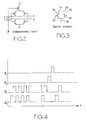
- Each of the memory devices 15 11 to 15 m2 and 25 11 to 25 n2 may be embodied as a complimentary latch of the type illustrated in Figure 2.
- the latch comprises a plurality of complimentary metal oxide on silicon field effect transistors arranged to function as a bi-stable element or flip-flop having normal and inverted inputs I, I, normal and inverted outputs O, O , and a clock input ⁇ .
- the switching elements 19 2 to 19 m and 28 2 to 28 n may each be embodied as shown in Figure 3.
- the switching element comprises an input 31 connected to the sources of metal oxide on silicon field effect transistors 32 and 33, first and second outputs 34 and 35 connected to the drains of the transistors 33 and 32, respectively, and complementary control inputs 36 and 37 connected to the gates of the transistors 32 and 33, respectively.
- the arrangements shown in Figures 2 and 3 are of known type and will not be described further.
- FIG. 4 is a timing diagram illustrating the two sets of bi-phase clock pulses ⁇ 1, ⁇ 2 and ⁇ 3, ⁇ 4.
- the clock pulses ⁇ 1 and ⁇ 2 are supplied to the lines 16 and 17 by the clock 18 in synchronism with serial display data supplied to the input 14 of the shift register 12.
- the clock pulses ⁇ 1 and ⁇ 2 are suspended and the bi-phase clock pulses ⁇ 3 and ⁇ 4 are supplied to the lines 26 and 27 by the clock 18 so that the shift register 24 supplies a strobe pulse to the next row or rows of pixels 10 ij .
- the row of display data is written into the corresponding row of pixels and is displayed until that row is again refreshed.
- the bi-phase clock pulses ⁇ 1 and ⁇ 2 are then supplied to the lines 16 and 17 so as to enter the next row of display data into the shift register 12. This process is repeated continuously so that the display is continuously refreshed on a row-by-row basis. When the last row R n has been refreshed, the process is repeated starting at the first row R 1 .
- Figure 5 illustrates operation of the display using the full spatial resolution of the display. Operation of the shift register 12 is illustrated, the operation of the shift register 24 being substantially identical.
- the binary display data are represented by the letters A, B, C, D, E.
- the switching elements 19 2 to 19 4 are controlled by the shift register 21 such that the clock inputs of the memory devices 15 21 to 15 41 are connected to the line 16 so as to receive the first phase clock pulses ⁇ 1 .
- the upper row of Figure 5 illustrates the application of a clock pulse ⁇ 2 which causes the data contained in the memory devices 15 22 to 15 42 to be equated to the data contained in the memory devices 15 21 to 15 41 , respectively.
- the middle row in Figure 5 illustrates the application of a clock pulse ⁇ 1 to the first memory devices 15 21 to 15 41 to perform a shift operation. This causes the data in each of the second memory devices to be written into the first memory device of the succeeding stage of the shift register. Thus, the bit D contained in the second memory device 15 12 of the stage 13 1 is written into the memory device 15 21 of the stage 13 2 , and so on.
- each stage 13 1 to 13 m of the shift register 12 contains a bit for individually controlling the corresponding pixel of the row of the display which is to be refreshed.
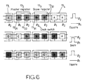
- Figure 6 is similar to Figure 5 but illustrates operation when reduced horizontal spatial resolution is required.
- the configuration data in the shift register 21 are such that the switching element 19 3 connects the clock input of the memory device 15 31 to the line 17 so as to receive the clock pulses ⁇ 2 .
- the stage 13 3 thus functions as a slave register whereas other stages, such as the stage 13 2 , functions as illustrated in Figure 5 as a master register.
- stage 13 3 differs in that it does not perform a shift function. Instead, whenever a clock pulse ⁇ 2 is supplied to perform the equate operation, both memory devices 15 31 and 15 32 of the stage 13 3 store the bit at the output of the second memory device 15 22 of the preceding stage 13 2 . Thus, apart from propagation and parasitic delays through the memory devices 15 31 and 15 32 , the address lines 11 2 and 11 3 receive simultaneously the same address data for the row of the display to be refreshed. The pixels 10 2j and 10 3j of the jth row being refreshed are thus addressed effectively as a single pixel of greater horizontal size and therefore of reduced horizontal resolution.
- the number of bi-phase clock pulses ⁇ 1 , ⁇ 2 required to refresh a display row is equal to the number of the stages of the shift register 12 acting as master registers. Accordingly, when operation with reduced horizontal resolution is required, the time needed to refresh each row is reduced so that the refresh rate of the display may be increased. Further, the reduced horizontal resolution requires a smaller amount of pixel display data to be calculated, for instance resulting in a reduced burden on a data processor controlling the display.
- the shift register 24 may be operated in the same way when reduced vertical resolution is required.
- each slave register repeats the bit stored in the preceding master register so that a row of display data is written substantially simultaneously to two of the rows of the display.
- the time required to refresh a frame of display data is proportional to the number of the stages of the shift register 24 acting as master registers so that operation to provide reduced vertical resolution increases the frame refresh rate of the display.
- the reduced resolution may result in a reduced burden of calculating display data by a data processor controlling the display.
- the pixels may effectively be partitioned into "rectangular" groups which receive the same display data and which are addressed as though they were single pixels of lower resolution. This is achieved without requiring any changes in conventional active matrix pixel addressing circuitry since the resolution is defined by the operation of the address generator circuitry.
- Figure 7 illustrates operation of the display to provide regions of different resolution.
- the stages of the shift registers 12 and 24 are shown schematically as empty squares representing stages acting as master registers, for instance as shown at 40, and shaded squares acting a slave registers, for instance as shown at 41.
- the pixels 10 are represented as empty squares corresponding to bright pixels and shaded squares corresponding to dark pixels.
- the data paths, for instance as shown at 42, indicate the propagation of data through the shift registers for each bi-phase clock pulse.
- data from a master register preceding a slave register is clocked substantially simultaneously into the slave register and into the succeeding master register.
- several consecutive stages may be operated as slave registers so that data from the preceding master register is clocked into all of the slave registers and into the succeeding master register substantially simultaneously.
- Pixels displaying an image at high resolution, corresponding to the full spatial resolution of the individual pixels, are illustrated at 43 and are located in regions addressed only by master registers in the shift registers 12 and 24.
- Low resolution regions, such as 44 are provided by pixels which are addressed by a master and one or more subsequent slave registers of both the shift register 12 and the shift register 24.
- a master register in each of the shift registers 12 and 24 is followed by a single slave register so that the effective pixel has half the resolution of the actual display pixels in both the vertical and horizontal directions.
- An intermediate resolution region is illustrated at 45.
- the pixels of this region are addressed by master registers of the shift register 12 and by a master and at least one slave registers of the shift register 24.
- the horizontal resolution is equal to the horizontal resolution of the display pixels but the vertical resolution is equal to half the vertical resolution of the display pixels.
- the pixels are addressed by contiguous columns and/or rows so as to form the rectangular groups effectively operating as single pixels.
- Reduced resolution operation is controlled by the patterns of binary data in the shift registers 21 and 30.
- the display resolution may therefore be reconfigured by changing the data held in the shift registers 21 and 30. This is achieved by serially entering fresh configuration data.
- the shift register 21 requires (m-1) bits of data to reconfigure the horizontal resolution whereas the shift register 30 requires (n-1) bits to reconfigure the vertical resolution.
- row data may be used instead of the strobing of pixel rows described hereinbefore by a "recirculating" strobe pulse.
- the arrangement shown in Figure 1 may be modified to achieve this by disconnecting the input of the stage 23 1 from the output of the stage 23 n and connecting it to a data input for receiving serial column data.
- the row and column data may then be read into the shift registers 12 and 24, respectively, and the whole SLM "strobed” to read the data into the pixels 10 ij simultaneously.
- Such an arrangement is useful where two dimensionally repeated patterns, such as holographic gratings are to be "displayed" by a SLM.
- each pixel has to be computed separately. This can take a very large amount of time, so typically where coarse resolution produces an adequate image, only a sparse number of pixels are computed to save time. It is known that, to match the coarse resolution of the computed image to that of the display, pixel values may be filled in either by interpolation techniques or simply by replication. This filling in and subsequent need for a very high specification display driver device would be unnecessary with the addressing scheme proposed. Since the proposed effective encoding of the display/SLM device is compatible with sparse computation of pixel points, a low specification display driver can be used, thus reducing hardware cost and physical size. The reduction in computation rate would also result in an energy saving as the energy consumption of microprocessors is roughly proportional to clock rate.
- an interlaced architecture is provided ( Figure 8). Such an architecture can be used with any of the above described addressing schemes.
- an interlaced shift register 60 is provided.
- the interlaced shift register 60 comprises a first and a second sub-shift register 61, 62, the stages of the first sub-shift register 61 being interlaced with the stages of the second sub-shift register 62.
- the first and second sub-shift registers 61, 62 are each of the same type as the shift register 12.
- the stages of the interlaced shift register 60 comprise first and second memory devices 60 11 , 60 12 to 60 m1 , 60 m2 .
- Each of the second memory devices 60 12 to 60 m2 has an output connected to the respective column addressing line 11 1 to 11 m and to the input of the first memory device 60 11 to 60 m1 of the succeeding shift register stage of the respective one of the sub-shift register 61, 62.
- the data input 14 comprises a first sub-data input 14a and a second sub-data input 14b.
- Serial display row data is split and processed in order to produce first and second serial display row data for the first and second sub-data inputs 14a, 14b, respectively.
- the second memory devices 60 12 to 60 m2 have clock inputs (not shown) connected to the second line 17 of the bi-phase clock line which receives clock signals ⁇ 2 from the clock 18.
- the first memory device 60 11 has a clock input (not shown) connected to the first line 16 of the bi-phase clock and receives clock signals ⁇ 1 from the clock 18.
- the first memory devices 60 21 to 60 m1 of the interlaced shift register 60 are connected (connections not shown) to the respective switching elements 19 2 to 19 m .
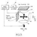
- a display of the type shown in Figure 1 or 8 may be used to provide a virtual reality (VR) headset as illustrated in Figure 9.
- Each eye 50 of the observer is provided with a reflective display 51 of the type shown in Figure 1 capable of providing variable resolution.
- the display is controlled by an image generator 52 which also controls red, green, and blue light emitting diodes 53 which are operated sequentially so as to provide a colour display to each eye.
- Light from the light emitting diodes 53 is collimated by a lens 54 and reflected by a beam splitter, such as a partially silvered mirror, onto the display 51, which spatially modulates the incident light.
- the light modulated with the image to be displayed is reflected from the display 51 through the beam splitter 55 and a lens 56 so that the image can be viewed by the eye 50.
- Light reflected from the eye 50 passes through the lens 56 and is reflected by the beam splitter 55 through a lens 57 to an eye-tracking charge coupled device (CCD) 58 so that an image of the eye 50 is formed on the CCD.
- CCD eye-tracking charge coupled device
- the output of the CCD is supplied to an eye tracker 59 which analyses the image of the eye so as to recognise the pupil and the part of the display 51 at which the eye is looking. This information is passed to the image generator 52.
- the image generator 52 controls the resolution of the display 51 so that the region at which the eye is looking i.e. the region imaged at and around the fovea of the eye, is operated at the full spatial resolution of the display whereas the remainder of the display is operated at reduced resolution.
- the red, green, and blue components of the colour image are supplied in sequence to the display 51 synchronously with operation of the RGB light emitting diodes 53.
- the image generator 52 also generates the image data which are to be displayed by the display 51.
- the image generator 52 effectively contains data concerning the positions of key points of the image to be displayed and software for performing predetermined rules for generating from those points the necessary image data.
- the image generator 52 thus calculates image data for all of the pixels in the region at which the eye is looking but generates sparse pixel image data corresponding to the reduced resolution for the remainder of the display.
- the processing power required by the image generator 52 to generate the image data is substantially reduced because it is only necessary to calculate pixels to high spatial resolution in the region which is being viewed by the eye. Other regions can be adequately represented by a reduced spatial density of pixels so that the number of calculations required to refresh each frame of the display can be substantially reduced. It is thus possible for very high resolution displays to be updated at video rates while making substantial savings in computation time and hence in required computation power and electrical power consumption.
- the display 51 of the type shown in Figure 1 may be replaced by a conventional very high resolution display provided that such a display is capable of being refreshed at normal video rates to avoid the visibility of undesirable visual artifacts.
- the image generator 52 operates in the same way to provide high resolution pixel data in the region of the display being viewed by the eye and reduced resolution image data for the remainder of the display. For instance, image data for a single pixel may be calculated at the middle of a group of pixels with that image data being duplicated in all of the display pixels. It is therefore possible to overcome processing limitations within the image generator 52 whether using a conventional very high resolution display or a variable resolution display of the type shown in Figure 1.
- the green image data may be used effectively as monochrome data and may be split in time between the updating of the 3 RGB subframes by updating every third course pixel with the low resolution green frame information per subframe.
- the colour sequential display shown in Figure 9 and comprising the display 51 and the light emitting diodes 53 could be replaced by a display in which fixed colour filters are provided as RGB triplets so that all colour data are displayed for each frame.
- the "course resolution" regions automatically amalgamate colours and minimal information is lost because of the colour blindness of the retinal cones in the human peripheral vision.
- the information of the green pixels would preferably be used to update the low resolution regions because this corresponds to the peak response of the receptors of the human eye.
- VR virtual reality
- the modified shift register update scheme can increase frame speeds for devices with very large pixel counts.
- Large pixel counts and update rates are required in the area of spatial light modulators for encoding coherent beams.
- This scheme is therefore particularly relevant for this area, especially since variable frame rates (a consequence of efficiently implementing the variable resolution scheme) are tolerated and simple alteration in resolution of a particular pattern can be of benefit (e.g. wavelength selection, angular beam scanning).
- Applications of coherent beam manipulation by SLMs include beam steering (e.g. laser printing), optical interconnections (e.g. fibre to fibre X-bar switches) and optical computing.
- variable aspect displays are possible that do not require complex data manipulation of the image data.
- grouping registers as described only two extra lines and possibly two pixels per line need be added to the data to display the correct image. This would require small alterations in addressing speed to allow near synchronous operation with the incoming data, thus possibly overcoming the need for local data storage.
- a display or SLM using this scheme can be programmed in software to be a conventional display, capable of addressing independently all pixels. This is important when considering compatibility with conventional systems.
Landscapes
- Engineering & Computer Science (AREA)
- Chemical & Material Sciences (AREA)
- Crystallography & Structural Chemistry (AREA)
- Physics & Mathematics (AREA)
- Computer Hardware Design (AREA)
- General Physics & Mathematics (AREA)
- Theoretical Computer Science (AREA)
- Control Of Indicators Other Than Cathode Ray Tubes (AREA)
- Liquid Crystal Display Device Control (AREA)
- Liquid Crystal (AREA)
Applications Claiming Priority (2)
| Application Number | Priority Date | Filing Date | Title |
|---|---|---|---|
| GB9613566 | 1996-06-27 | ||
| GB9613566A GB2314664A (en) | 1996-06-27 | 1996-06-27 | Address generator,display and spatial light modulator |
Publications (3)
| Publication Number | Publication Date |
|---|---|
| EP0821338A2 true EP0821338A2 (de) | 1998-01-28 |
| EP0821338A3 EP0821338A3 (de) | 1998-11-11 |
| EP0821338B1 EP0821338B1 (de) | 2002-03-06 |
Family
ID=10796032
Family Applications (1)
| Application Number | Title | Priority Date | Filing Date |
|---|---|---|---|
| EP97304638A Expired - Lifetime EP0821338B1 (de) | 1996-06-27 | 1997-06-27 | Adressgenerator für Anzeige und Lichtmodulator mit rekonfigurierbarem Schieberegister |
Country Status (5)
| Country | Link |
|---|---|
| US (1) | US6175352B1 (de) |
| EP (1) | EP0821338B1 (de) |
| JP (1) | JP3957012B2 (de) |
| DE (1) | DE69710820T2 (de) |
| GB (1) | GB2314664A (de) |
Cited By (5)
| Publication number | Priority date | Publication date | Assignee | Title |
|---|---|---|---|---|
| WO2000038166A1 (en) * | 1998-12-19 | 2000-06-29 | The Secretary Of State For Defence | Active backplane circuitry, spatial light modulator comprising such a circuitry, and method of operating such a spatial light modulator |
| KR100487389B1 (ko) * | 2001-11-30 | 2005-05-03 | 샤프 가부시키가이샤 | 신호선 구동회로 및 그를 사용한 표시장치 |
| US7202846B2 (en) | 2001-11-30 | 2007-04-10 | Sharp Kabushiki Kaisha | Signal line drive circuit and display device using the same |
| US7372444B2 (en) | 2003-05-26 | 2008-05-13 | Seiko Epson Corporation | Semiconductor integrated circuit |
| US7652652B2 (en) * | 2002-11-12 | 2010-01-26 | Sharp Kabushiki Kaisha | Data signal line driving method, data signal line driving circuit, and display device using the same |
Families Citing this family (36)
| Publication number | Priority date | Publication date | Assignee | Title |
|---|---|---|---|---|
| JP2000227784A (ja) * | 1998-07-29 | 2000-08-15 | Seiko Epson Corp | 電気光学装置の駆動回路および電気光学装置 |
| US6559971B1 (en) * | 1998-10-27 | 2003-05-06 | Hewlett-Packard Development Co., L.P. | Self-resizing demonstration page for a printing device |
| JP3999432B2 (ja) * | 2000-02-08 | 2007-10-31 | 富士フイルム株式会社 | 画像処理方法および装置並びに記録媒体 |
| US6456262B1 (en) * | 2000-05-09 | 2002-09-24 | Intel Corporation | Microdisplay with eye gaze detection |
| JP2002203397A (ja) * | 2000-10-24 | 2002-07-19 | Alps Electric Co Ltd | シフトレジスタ回路、表示装置およびイメージセンサ |
| US6927753B2 (en) * | 2000-11-07 | 2005-08-09 | Semiconductor Energy Laboratory Co., Ltd. | Display device |
| WO2002065443A1 (en) * | 2001-02-15 | 2002-08-22 | Tveye Inc. | Method and apparatus for low bandwidth transmission of data utilizing of the human eye anatomy |
| US20030128324A1 (en) * | 2001-11-27 | 2003-07-10 | Woods Daniel D. | Pixel size enhancements |
| US7317464B2 (en) * | 2002-08-21 | 2008-01-08 | Intel Corporation | Pulse width modulated spatial light modulators with offset pulses |
| TW566416U (en) * | 2003-04-22 | 2003-12-11 | Shi-Tsai Chen | Air expanding shaft |
| GB0510470D0 (en) | 2005-05-23 | 2005-06-29 | Qinetiq Ltd | Coded aperture imaging system |
| GB2434935A (en) | 2006-02-06 | 2007-08-08 | Qinetiq Ltd | Coded aperture imager using reference object to form decoding pattern |
| GB2434937A (en) | 2006-02-06 | 2007-08-08 | Qinetiq Ltd | Coded aperture imaging apparatus performing image enhancement |
| GB2434877A (en) | 2006-02-06 | 2007-08-08 | Qinetiq Ltd | MOEMS optical modulator |
| GB0602380D0 (en) | 2006-02-06 | 2006-03-15 | Qinetiq Ltd | Imaging system |
| GB2434934A (en) | 2006-02-06 | 2007-08-08 | Qinetiq Ltd | Processing coded aperture image data by applying weightings to aperture functions and data frames |
| GB2434936A (en) | 2006-02-06 | 2007-08-08 | Qinetiq Ltd | Imaging system having plural distinct coded aperture arrays at different mask locations |
| GB0615040D0 (en) | 2006-07-28 | 2006-09-06 | Qinetiq Ltd | Processing method for coded apperture sensor |
| BR112012022747A2 (pt) * | 2010-03-12 | 2016-07-19 | Qualcomm Mems Technologies Inc | multiplicação de linha para permitir taxa de restauração aumentada de um monitor |
| US8698859B2 (en) * | 2010-10-19 | 2014-04-15 | Blackberry Limited | Display screen having regions of differing pixel density |
| KR101592272B1 (ko) | 2010-12-28 | 2016-02-18 | 인디안 인스티튜트 오브 테크놀로지 칸푸르 | 수렴 매트릭스 인수분해 기반 전체 프레임 이미지 처리 |
| US9265458B2 (en) | 2012-12-04 | 2016-02-23 | Sync-Think, Inc. | Application of smooth pursuit cognitive testing paradigms to clinical drug development |
| US9380976B2 (en) | 2013-03-11 | 2016-07-05 | Sync-Think, Inc. | Optical neuroinformatics |
| US20140280502A1 (en) | 2013-03-15 | 2014-09-18 | John Cronin | Crowd and cloud enabled virtual reality distributed location network |
| US20140280505A1 (en) | 2013-03-15 | 2014-09-18 | John Cronin | Virtual reality interaction with 3d printing |
| US20140280506A1 (en) | 2013-03-15 | 2014-09-18 | John Cronin | Virtual reality enhanced through browser connections |
| US9838506B1 (en) | 2013-03-15 | 2017-12-05 | Sony Interactive Entertainment America Llc | Virtual reality universe representation changes viewing based upon client side parameters |
| US20140280644A1 (en) | 2013-03-15 | 2014-09-18 | John Cronin | Real time unified communications interaction of a predefined location in a virtual reality location |
| US20140267581A1 (en) | 2013-03-15 | 2014-09-18 | John Cronin | Real time virtual reality leveraging web cams and ip cams and web cam and ip cam networks |
| US20140280503A1 (en) | 2013-03-15 | 2014-09-18 | John Cronin | System and methods for effective virtual reality visitor interface |
| US9588343B2 (en) | 2014-01-25 | 2017-03-07 | Sony Interactive Entertainment America Llc | Menu navigation in a head-mounted display |
| US9437159B2 (en) | 2014-01-25 | 2016-09-06 | Sony Interactive Entertainment America Llc | Environmental interrupt in a head-mounted display and utilization of non field of view real estate |
| KR102367788B1 (ko) | 2014-03-14 | 2022-02-24 | 가부시키가이샤 한도오따이 에네루기 켄큐쇼 | 아날로그 연산 회로, 반도체 장치, 및 전자 기기 |
| KR102245297B1 (ko) | 2014-05-15 | 2021-04-27 | 삼성전자주식회사 | 단일 방향성의 빔을 이용한 영상 표시 장치 및 방법 |
| KR102462110B1 (ko) | 2016-03-15 | 2022-11-03 | 삼성디스플레이 주식회사 | 게이트 구동부 및 이를 포함하는 표시 장치 |
| GB2563832B (en) * | 2017-06-23 | 2021-11-10 | Sony Interactive Entertainment Inc | Display method and apparatus |
Family Cites Families (22)
| Publication number | Priority date | Publication date | Assignee | Title |
|---|---|---|---|---|
| JPS55146489A (en) * | 1979-04-20 | 1980-11-14 | Suwa Seikosha Kk | Liquid crystal matrix display unit |
| US4348186A (en) | 1979-12-17 | 1982-09-07 | The United States Of America As Represented By The Secretary Of The Navy | Pilot helmet mounted CIG display with eye coupled area of interest |
| JPS6061796A (ja) * | 1983-09-16 | 1985-04-09 | シャープ株式会社 | 表示装置 |
| FR2558979B1 (fr) | 1984-01-31 | 1986-05-23 | Commissariat Energie Atomique | Procede d'adressage au moyen de registres a decalage formes de memoires statiques d'un imageur matriciel |
| US4634384A (en) | 1984-02-02 | 1987-01-06 | General Electric Company | Head and/or eye tracked optically blended display system |
| GB8728435D0 (en) | 1987-12-04 | 1988-01-13 | Emi Plc Thorn | Display device |
| US5266936A (en) | 1989-05-09 | 1993-11-30 | Nec Corporation | Driving circuit for liquid crystal display |
| US5339090A (en) * | 1989-06-23 | 1994-08-16 | Northern Telecom Limited | Spatial light modulators |
| US5206634A (en) | 1990-10-01 | 1993-04-27 | Sharp Kabushiki Kaisha | Liquid crystal display apparatus |
| US5204661A (en) | 1990-12-13 | 1993-04-20 | Xerox Corporation | Input/output pixel circuit and array of such circuits |
| GB2259213A (en) | 1991-08-29 | 1993-03-03 | British Aerospace | Variable resolution view-tracking display |
| JP3147973B2 (ja) | 1992-03-09 | 2001-03-19 | 株式会社 沖マイクロデザイン | 駆動回路 |
| GB9207527D0 (en) | 1992-04-07 | 1992-05-20 | Philips Electronics Uk Ltd | Multi-standard video matrix display apparatus and its method of operation |
| JPH05303362A (ja) * | 1992-04-28 | 1993-11-16 | Sharp Corp | 表示装置 |
| JP2815102B2 (ja) | 1992-08-26 | 1998-10-27 | シャープ株式会社 | アクティブマトリクス型液晶表示装置 |
| US5859627A (en) * | 1992-10-19 | 1999-01-12 | Fujitsu Limited | Driving circuit for liquid-crystal display device |
| JP2735451B2 (ja) * | 1993-01-05 | 1998-04-02 | 日本電気株式会社 | マルチスキャン型液晶ディスプレイ装置 |
| JP2896291B2 (ja) * | 1993-06-14 | 1999-05-31 | 株式会社エイ・ティ・アール通信システム研究所 | 画像表示装置 |
| JP3329009B2 (ja) | 1993-06-30 | 2002-09-30 | ソニー株式会社 | アクティブマトリクス表示装置 |
| JP3243932B2 (ja) | 1994-04-22 | 2002-01-07 | ソニー株式会社 | アクティブマトリクス表示装置 |
| DE19541301C1 (de) * | 1995-11-06 | 1997-06-05 | Siemens Ag | Medizindiagnostikeinrichtung |
| JPH09305156A (ja) * | 1996-05-16 | 1997-11-28 | Nippon Telegr & Teleph Corp <Ntt> | 映像表示方法及び装置 |
-
1996
- 1996-06-27 GB GB9613566A patent/GB2314664A/en not_active Withdrawn
-
1997
- 1997-06-26 US US08/883,508 patent/US6175352B1/en not_active Expired - Fee Related
- 1997-06-26 JP JP17069797A patent/JP3957012B2/ja not_active Expired - Fee Related
- 1997-06-27 EP EP97304638A patent/EP0821338B1/de not_active Expired - Lifetime
- 1997-06-27 DE DE69710820T patent/DE69710820T2/de not_active Expired - Lifetime
Cited By (6)
| Publication number | Priority date | Publication date | Assignee | Title |
|---|---|---|---|---|
| WO2000038166A1 (en) * | 1998-12-19 | 2000-06-29 | The Secretary Of State For Defence | Active backplane circuitry, spatial light modulator comprising such a circuitry, and method of operating such a spatial light modulator |
| US7061463B2 (en) | 1998-12-19 | 2006-06-13 | Qinetiq Limited | Addressing technique for an active backplane device |
| KR100487389B1 (ko) * | 2001-11-30 | 2005-05-03 | 샤프 가부시키가이샤 | 신호선 구동회로 및 그를 사용한 표시장치 |
| US7202846B2 (en) | 2001-11-30 | 2007-04-10 | Sharp Kabushiki Kaisha | Signal line drive circuit and display device using the same |
| US7652652B2 (en) * | 2002-11-12 | 2010-01-26 | Sharp Kabushiki Kaisha | Data signal line driving method, data signal line driving circuit, and display device using the same |
| US7372444B2 (en) | 2003-05-26 | 2008-05-13 | Seiko Epson Corporation | Semiconductor integrated circuit |
Also Published As
| Publication number | Publication date |
|---|---|
| EP0821338B1 (de) | 2002-03-06 |
| GB9613566D0 (en) | 1996-08-28 |
| JP3957012B2 (ja) | 2007-08-08 |
| DE69710820T2 (de) | 2002-10-02 |
| JPH1069252A (ja) | 1998-03-10 |
| EP0821338A3 (de) | 1998-11-11 |
| US6175352B1 (en) | 2001-01-16 |
| DE69710820D1 (de) | 2002-04-11 |
| GB2314664A (en) | 1998-01-07 |
Similar Documents
| Publication | Publication Date | Title |
|---|---|---|
| EP0821338B1 (de) | Adressgenerator für Anzeige und Lichtmodulator mit rekonfigurierbarem Schieberegister | |
| US5751264A (en) | Distributed duty-cycle operation of digital light-modulators | |
| KR100346878B1 (ko) | 블럭리셋및보조메모리로다중화된메모리타이밍 | |
| US5225823A (en) | Field sequential liquid crystal display with memory integrated within the liquid crystal panel | |
| EP0530762B1 (de) | Steuersystem für eine DMD-Anzeige | |
| JP3084293B2 (ja) | ピクセル反転動作を伴うlcdドライバic | |
| US5670973A (en) | Method and apparatus for compensating crosstalk in liquid crystal displays | |
| EP0547601B1 (de) | Farbanzeigevorrichtung unter Verwendung räumlichen Modulatoren | |
| US7903104B2 (en) | Spatial modulator display system using two memories and display time slices having differing times | |
| JP3253481B2 (ja) | メモリインターフェイス回路 | |
| EP0848369A2 (de) | Lichtmodulationsvorrichtungen | |
| US5877740A (en) | Display device | |
| KR20230107353A (ko) | 최적화된 전력 및 면적을 갖는 픽셀을 구동하기 위한 시스템 및 방법 | |
| JP4612952B2 (ja) | グレイスケール画像表示のための複数デジタル・ビットプレーンの高速読出し | |
| EP0755556B1 (de) | Verfahren und einrichtung zum steuern einer anzeigevorrichtung | |
| JP3133414B2 (ja) | カラー液晶表示方式 | |
| US6850218B2 (en) | Frame prewriting in a liquid crystal display | |
| JP3935209B2 (ja) | デジタル光変調器の多フレーム速度作動 | |
| EP1402512A1 (de) | Adressierung einer anordnung von anzeigeelementen | |
| JP2004533018A5 (de) | ||
| US20020145580A1 (en) | Minimizing frame writing time of a liquid crystal display | |
| JP3515699B2 (ja) | ディジタルディスプレイ装置およびその駆動方法 | |
| JP2006017797A (ja) | 平面表示装置のデータ側駆動回路 | |
| CN121729730A (zh) | 光学菱形通带滤波器 | |
| JPH0915558A (ja) | 液晶表示装置 |
Legal Events
| Date | Code | Title | Description |
|---|---|---|---|
| PUAI | Public reference made under article 153(3) epc to a published international application that has entered the european phase |
Free format text: ORIGINAL CODE: 0009012 |
|
| AK | Designated contracting states |
Kind code of ref document: A2 Designated state(s): DE FR GB |
|
| PUAL | Search report despatched |
Free format text: ORIGINAL CODE: 0009013 |
|
| AK | Designated contracting states |
Kind code of ref document: A3 Designated state(s): AT BE CH DE DK ES FI FR GB GR IE IT LI LU MC NL PT SE |
|
| 17P | Request for examination filed |
Effective date: 19990510 |
|
| AKX | Designation fees paid |
Free format text: DE FR GB |
|
| 17Q | First examination report despatched |
Effective date: 20000313 |
|
| GRAG | Despatch of communication of intention to grant |
Free format text: ORIGINAL CODE: EPIDOS AGRA |
|
| GRAG | Despatch of communication of intention to grant |
Free format text: ORIGINAL CODE: EPIDOS AGRA |
|
| GRAG | Despatch of communication of intention to grant |
Free format text: ORIGINAL CODE: EPIDOS AGRA |
|
| GRAH | Despatch of communication of intention to grant a patent |
Free format text: ORIGINAL CODE: EPIDOS IGRA |
|
| GRAH | Despatch of communication of intention to grant a patent |
Free format text: ORIGINAL CODE: EPIDOS IGRA |
|
| REG | Reference to a national code |
Ref country code: GB Ref legal event code: IF02 |
|
| GRAA | (expected) grant |
Free format text: ORIGINAL CODE: 0009210 |
|
| AK | Designated contracting states |
Kind code of ref document: B1 Designated state(s): DE FR GB |
|
| REF | Corresponds to: |
Ref document number: 69710820 Country of ref document: DE Date of ref document: 20020411 |
|
| ET | Fr: translation filed | ||
| PLBE | No opposition filed within time limit |
Free format text: ORIGINAL CODE: 0009261 |
|
| STAA | Information on the status of an ep patent application or granted ep patent |
Free format text: STATUS: NO OPPOSITION FILED WITHIN TIME LIMIT |
|
| 26N | No opposition filed |
Effective date: 20021209 |
|
| PGFP | Annual fee paid to national office [announced via postgrant information from national office to epo] |
Ref country code: FR Payment date: 20100709 Year of fee payment: 14 |
|
| PGFP | Annual fee paid to national office [announced via postgrant information from national office to epo] |
Ref country code: GB Payment date: 20100623 Year of fee payment: 14 Ref country code: DE Payment date: 20100625 Year of fee payment: 14 |
|
| GBPC | Gb: european patent ceased through non-payment of renewal fee |
Effective date: 20110627 |
|
| REG | Reference to a national code |
Ref country code: FR Ref legal event code: ST Effective date: 20120229 |
|
| REG | Reference to a national code |
Ref country code: DE Ref legal event code: R119 Ref document number: 69710820 Country of ref document: DE Effective date: 20120103 |
|
| PG25 | Lapsed in a contracting state [announced via postgrant information from national office to epo] |
Ref country code: DE Free format text: LAPSE BECAUSE OF NON-PAYMENT OF DUE FEES Effective date: 20120103 Ref country code: FR Free format text: LAPSE BECAUSE OF NON-PAYMENT OF DUE FEES Effective date: 20110630 |
|
| PG25 | Lapsed in a contracting state [announced via postgrant information from national office to epo] |
Ref country code: GB Free format text: LAPSE BECAUSE OF NON-PAYMENT OF DUE FEES Effective date: 20110627 |