EP0821396A2 - Verfahren und Gerät zur Messung der Ätzgleichmässigkeit eines Halbleiters - Google Patents
Verfahren und Gerät zur Messung der Ätzgleichmässigkeit eines Halbleiters Download PDFInfo
- Publication number
- EP0821396A2 EP0821396A2 EP97304913A EP97304913A EP0821396A2 EP 0821396 A2 EP0821396 A2 EP 0821396A2 EP 97304913 A EP97304913 A EP 97304913A EP 97304913 A EP97304913 A EP 97304913A EP 0821396 A2 EP0821396 A2 EP 0821396A2
- Authority
- EP
- European Patent Office
- Prior art keywords
- data
- value
- uniformity
- derivative
- point
- Prior art date
- Legal status (The legal status is an assumption and is not a legal conclusion. Google has not performed a legal analysis and makes no representation as to the accuracy of the status listed.)
- Withdrawn
Links
Images



Classifications
-
- H—ELECTRICITY
- H01—ELECTRIC ELEMENTS
- H01J—ELECTRIC DISCHARGE TUBES OR DISCHARGE LAMPS
- H01J37/00—Discharge tubes with provision for introducing objects or material to be exposed to the discharge, e.g. for the purpose of examination or processing thereof
- H01J37/32—Gas-filled discharge tubes
- H01J37/32917—Plasma diagnostics
- H01J37/32935—Monitoring and controlling tubes by information coming from the object and/or discharge
-
- H—ELECTRICITY
- H01—ELECTRIC ELEMENTS
- H01J—ELECTRIC DISCHARGE TUBES OR DISCHARGE LAMPS
- H01J37/00—Discharge tubes with provision for introducing objects or material to be exposed to the discharge, e.g. for the purpose of examination or processing thereof
- H01J37/32—Gas-filled discharge tubes
- H01J37/32917—Plasma diagnostics
- H01J37/32935—Monitoring and controlling tubes by information coming from the object and/or discharge
- H01J37/32972—Spectral analysis
-
- H—ELECTRICITY
- H01—ELECTRIC ELEMENTS
- H01J—ELECTRIC DISCHARGE TUBES OR DISCHARGE LAMPS
- H01J37/00—Discharge tubes with provision for introducing objects or material to be exposed to the discharge, e.g. for the purpose of examination or processing thereof
- H01J37/32—Gas-filled discharge tubes
- H01J37/32917—Plasma diagnostics
- H01J37/3299—Feedback systems
-
- H—ELECTRICITY
- H01—ELECTRIC ELEMENTS
- H01J—ELECTRIC DISCHARGE TUBES OR DISCHARGE LAMPS
- H01J2237/00—Discharge tubes exposing object to beam, e.g. for analysis treatment, etching, imaging
- H01J2237/32—Processing objects by plasma generation
- H01J2237/33—Processing objects by plasma generation characterised by the type of processing
- H01J2237/334—Etching
Definitions
- the invention relates to semiconductor wafer processing systems that perform "dry" etching of semiconductor wafers. More particularly, the invention relates to a method and apparatus for performing in situ measurement of etch uniformity as a semiconductor wafer is etched by a semiconductor processing system.
- Semiconductor processing systems that perform "dry" etch of semiconductor wafers typically rely upon post processing analysis to determine the uniformity of the etch process.
- a plurality of wafers are etched and then the amount of material removed by the etch process is measured using depth-measuring equipment, such as a laser interferometer for transparent films or profilometer for opaque films.
- the measuring equipment measures the etch results at various points on the wafer surface. The relative depth of each point provides an indication of etch uniformity.
- Such wafer post processing is expensive and consumes many wafers before the uniformity produced by the etch process is satisfactory.
- the '356 invention must make certain assumptions concerning the etch rate and the thickness of the wafer films in order to predict the uniformity at any point during the etch process. Such assumptions can be error prone.
- the present invention analyzes optical emission spectroscopy (OES) data produced by an etch rate monitoring system.
- the invention computes the first derivative of the OES data as the data is acquired.
- a trigger criterion i.e., a trigger point
- the invention correlates the value of the first derivative with a particular uniformity value.
- the correlation can be accomplished using a look-up table or a correlation equation.
- the look-up table or correlation equation are predefined using empirical data.
- the invention then displays the uniformity value and/or responds in some manner to the uniformity value.
- the present invention has been found to accurately predict etch uniformity using this direct, in situ measurement technique. As such, extensive post-processing is not necessary which substantially reduces the costs associated with performing an etch process.
- the present invention is a method and apparatus for performing a direct, in situ measurement of etch uniformity of a semiconductor wafer within a semiconductor wafer processing system.
- the invention analyzes optical emission spectroscopy (OES) data collected as a semiconductor wafer is being etched within an etching system, such as Model PE5000 manufactured by Applied Materials, Inc. of Santa Clara, California.
- OES data may be collected by any type of in situ measuring equipment that provides accurate OES data.
- Such a system is the OES endpoint system manufactured by Applied Materials, Inc. as an integrated emissions endpoint module for the Model PE5000.
- an OES system is illustratively used for data acquisition, the invention can be used with any system that produces data that indicates etch process progression, e.g., interferometric systems.
- the following discussion presents the invention as adapted to operate within an OES system. From this disclosure, those skilled could adapt the invention to operate within other forms of etch process monitoring system.
- FIG. 1 depicts a block diagram of an OES system 100, also known as an optical emission endpoint detection system.
- the hardware of this system is conventionally used for endpoint detection, whereby data is collected from a monochromator module 110 as it monitors a particular wavelength of emitted light from a plasma in a process chamber 102. A particular change in the intensity of an emission at the monitored wavelength is indicative of the endpoint for the etch process.
- a typical endpoint detection system is disclosed in U.S. Patent 5,362,356, issued November 8, 1994.
- Further processing and analysis of a particular wavelength emission e.g., the carbon-monoxide (CO) emission line at 4835 angstroms
- the invention is implemented in software within a computer system that processes and analyzes the OES data to deduce the etch uniformity across the wafer surface.
- FIG. 1 depicts a process chamber 102 of, for example, a PE5000 etching system 100 connected by a fiber optic cable 103 to the integrated emissions endpoint module 101.
- the integrated emissions endpoint module contains a monochromator module 110, controller electronics 118 and a computer system 122.
- the monochromator module further contains a monochromator 104, a stepper motor 112 for controlling the wavelength selection for the monochromator, a calibration lamp 114 for calibrating the monochromator, a photomultiplier tube 106, a high-voltage power supply 108, and a monochromator interface board 116.
- light generated by a plasma within the process chamber 102 is coupled to the monochromator through the fiber optic cable 103.
- the monochromator converts the photons carried by the fiber optic cable 103 into electrons.
- the electrons are multiplied by the photomultiplier tube 106 that is powered by the high-voltage power supply 108.
- the output of the photomultiplier tube 106 is coupled to the monochromator interface board 116.
- the monochromator interface board 116 controls the stepper motor 112 that selects a particular light wavelength for processing.
- the stepper motor controls the position of an interference grid (not shown) within the monochromator to select a particular wavelength of light for analysis.
- the calibration lamp 114 is coupled to the monochromator to calibrate the monochromator at a particular wavelength.
- a DB-25 electrical cable connects the monochromator interface board 116 to the controller interface board 120 within controller electronics 118
- the control electronics are coupled to the computer system 122 via a computer bus 126, e.g., a serial bus.
- a computer bus 126 e.g., a serial bus.
- the conventional endpoint software 128, as well as the etch uniformity derivation software 124 of the present invention and the computer operating system 130, are stored within and executed by the computer system 122.
- the hardware for implementing the foregoing integrated emission endpoint module 101 is available from Applied Materials, Inc. of Santa Clara, California.
- the fiber optic cable is available from Applied Materials, Inc. as part number 0190-09134, the monochromator as part number 0010-09935, the controller electronics as part number 0240-10475, and the computer system as part number 0240-32585.
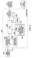
- FIG. 2 depicts a detailed block diagram of the computer system 122 which facilitates OES data analysis, processing and display.
- the computer 200 contains a central processing unit (CPU) 204, support circuitry 206, random access memory (RAM) 208, read only memory (ROM) 212, mass storage device 214 (e.g., a disk drive), and a display driver 216.
- a user interacts with the computer system through one or more input devices 220, such as a keyboard, mouse, trackball, touch pad, and the like.
- the computer system displays the data, various graphical interface displays, and the uniformity value(s) on an output display device 218, such as a computer monitor.
- the computer system may also interact with other output display devices, such as a printer, to provide hard copy of any display that appears on the computer monitor.
- the controller interface board 120 preprocesses the data from the monochromator module 110 and provides data transport between the monochromator module and the CPU 204
- the CPU 204 is a general purpose processor such as a PowerPC, Pentium, or some other generally available processor.
- PowerPC is a registered trademark of International Business Machines of Armonk, New York
- Pentium is a registered trademark of Intel Corporation, of Santa Clara, California. Since the software implementation of the present invention is not required to execute on any specific processor, routines implementing the present invention can be executed upon any type of processor or combination of processors in a parallel processing computer environment.
- the present embodiment of the invention described herein executes on a Pentium processor that is manufactured by Intel Corporation, of Santa Clara, California.
- the CPU 204 operates in conjunction with various other circuits such as RAM 208, ROM 212, storage device 214 and support circuitry 206 such as co-processors, clock circuits, cache, power supplies and other well known circuits.
- RAM 208 random access memory
- ROM 212 read-only memory
- storage device 214 storage device
- support circuitry 206 such as co-processors, clock circuits, cache, power supplies and other well known circuits.
- the operation and interrelationship of the various computer components contained in general purpose computer are well known in the art and do not require further explanation.
- the display driver 216 may be a video card, printer driver, or other common driver software and hardware as required by the output device 218.
- the RAM 208 stores the software implementation of the present invention, i.e., the etch uniformity derivation routine 124.
- the routines of the invention are stored in the mass storage device 214 and recalled for temporary storage in RAM while being executed by the CPU 204.
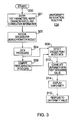
- FIG. 3 depicts a flow diagram of the etch uniformity derivation routine 124 of the present invention.
- the routine begins at step 300 and proceeds to step 301.
- a user initializes test parameters, wafer characteristics, and various correlation parameters. Such initialization can be accomplished by entering the information via the computer system input device(s) or by recalling the information from memory.
- the routine receives OES data from the monochromator module.
- the routine processes the OES data. This processing averages the data points to produce a smooth data set that, when plotted, would generate a smooth curve representing the magnitude of the OES data versus time.
- a rolling average is used to include additional data points into the average as the data is available from the monochromator module.
- Further processing may include data thresholding, spike filtering and the like.
- the combination of the system initialization and data acquisition steps form a data acquisition module of the invention.
- An illustrative OES data curve produced by this module is depicted in FIG. 4 as curve 400.
- This curve represents the magnitude of the OES data normalized as a percentage of the full scale of the data acquisition equipment (the right-hand scale) versus time, in seconds.
- the routine 124 computes a first derivative of the data.
- This step of the routine forms a derivative generator that generates the first derivative by taking a pair of sequential and filtered data points and dividing by the time elapsed between those two filtered data points. The routine repeats this computation as each filtered data point is generated by the monochromator module.
- the first derivative is: X 2 - X 1 ⁇ T where X 1 is a first filtered data point, and X 2 is a second filtered data point and ⁇ T is the time duration between the X 1 and X 2 .
- ⁇ T is typically 0.1 seconds.
- Curve 402 represents the first derivative as a change in the full scale percentage (normalized data values) over a specific time duration ⁇ T (left-hand scale) versus time. The peak of curve 402 indicates the inflection point of the OES data curve 400.
- the routine detects the "trigger point" of the OES data curve.
- the trigger point is user selected during system initialization in step 302.
- This trigger point selection step forms a trigger criterion generator.
- the trigger point can be any point on the OES data curve; however, the selection is usually the inflection point in the OES data curve or the etch endpoint of the OES data curve.
- the etch endpoint is generally defined by the parameters selected to control the endpoint software. Specifically, the value of the first derivative of the OES data at the inflection point repeatably correlates with the etch uniformity across the wafer. Furthermore, if the etching process is stopped before the inflection point is reached, the value of the first derivative at the point where etching is halted (i.e., the endpoint) is indicative of the uniformity across the wafer at that point in time.
- the correlation between etch uniformity and the magnitude of the first derivative depends upon the test parameters used as well as the wafer characteristics and wafer recipe. Consequently, the test parameters and wafer characteristics are preloaded at step 301, into the memory of the computer system such that they can be selected by the user at test initiation. Generally, the user will select the present test parameters and wafer characteristics from a menu and a look-up-table associated with those parameters is loaded into memory.
- the look-up table is a correlation table for values of first derivative and uniformity.
- the routine accesses the look-up table containing the uniformity versus first derivative correlation values. The table access process that correlates first derivative values and uniformity values forms a data analyzer.
- the routine uses this look-up table and given a value of the first derivative, the routine generates a uniformity value for the wafer that corresponds to the wafer characteristics and the test parameters of the present test.
- a correlation equation is used rather than a look-up table. A graphical representation of an illustrative correlation equation is depicted and described in relation to FIG. 5.
- the routine displays the uniformity value.
- the uniformity value may be compared to a threshold and, depending upon the uniformity value with respect to the threshold, the routine generates a subjective uniformity term such as uniformity "good” or uniformity "poor".
- the routine may compare the uniformity value with a plurality of threshold values where, depending on the particular threshold value that is exceeded by the uniformity value, the routine can make suggestions on how to improve the uniformity. For example, for very poor uniformity, the routine may suggest that the user accomplish a preventive maintenance procedure such as cleaning chamber windows, recalibration of the monochromator and the like.
- FIG. 5 depicts a graph 500 of etch uniformity (scale 502) versus normalized first derivative values (scale 504) corresponding to a particular test parameter and wafer characteristic set.
- the first derivative values shown are the "peak" values at the inflection point, also known as the "minimum slope” values.
- an etch process that attains a minimum slope of -2 would have a coefficient of variation (a measure of uniformity) of 2 percent.
- a look-up table containing the information in the graph of FIG. 5 would be used at step 312 of the flow diagram to determine the uniformity given a particular value of first derivatives.
- a curve fitted to the data points (e.g., curve 506) is used to derive an equation from which any value of uniformity can be derived from a given minimum slope value.
- the film thickness measurements used to generate curve 500 were performed using the Prometrix SM-300 and measuring 49 points with a 6 mm edge exclusion before and after etching.
- the wafers were 150 mm thermal oxide wafers.
- the test was conducted within a process chamber containing a pressure of 200 mTorr, the cathode temperature was maintained at 20 degree Celsius and 8 Torr of Helium was provided to cool the backside of the wafer.
- the chamber was provided a 25 sccm flow of CHF 3 , a 5 sccm flow of CF 4 , and a 75 sccm flow of Ar.
- the plasma was powered by 750 Watts and a 30 G magnetic containment field was used.
- the etch non-uniformity is represented in FIG.
- CV coefficient of variation
- the routine may control the etch process such that the etching of the wafer is concluded when a particular uniformity is reached and after a particular etch rate has been exceeded, thus providing a means of optimally controlling the wafer etch process.
Landscapes
- Physics & Mathematics (AREA)
- Engineering & Computer Science (AREA)
- Plasma & Fusion (AREA)
- Chemical & Material Sciences (AREA)
- Analytical Chemistry (AREA)
- Spectroscopy & Molecular Physics (AREA)
- Drying Of Semiconductors (AREA)
- Investigating, Analyzing Materials By Fluorescence Or Luminescence (AREA)
- Testing Or Measuring Of Semiconductors Or The Like (AREA)
- ing And Chemical Polishing (AREA)
Applications Claiming Priority (2)
| Application Number | Priority Date | Filing Date | Title |
|---|---|---|---|
| US686229 | 1996-07-23 | ||
| US08/686,229 US6649075B1 (en) | 1996-07-23 | 1996-07-23 | Method and apparatus for measuring etch uniformity of a semiconductor wafer |
Publications (2)
| Publication Number | Publication Date |
|---|---|
| EP0821396A2 true EP0821396A2 (de) | 1998-01-28 |
| EP0821396A3 EP0821396A3 (de) | 2000-09-20 |
Family
ID=24755463
Family Applications (1)
| Application Number | Title | Priority Date | Filing Date |
|---|---|---|---|
| EP97304913A Withdrawn EP0821396A3 (de) | 1996-07-23 | 1997-07-04 | Verfahren und Gerät zur Messung der Ätzgleichmässigkeit eines Halbleiters |
Country Status (5)
| Country | Link |
|---|---|
| US (1) | US6649075B1 (de) |
| EP (1) | EP0821396A3 (de) |
| JP (1) | JPH1074674A (de) |
| KR (1) | KR980012213A (de) |
| TW (1) | TW355825B (de) |
Cited By (2)
| Publication number | Priority date | Publication date | Assignee | Title |
|---|---|---|---|---|
| WO1999004425A1 (de) * | 1997-07-17 | 1999-01-28 | Robert Bosch Gmbh | Verfahren zum erkennen des übergangs verschiedener materialien in halbleiterstrukturen |
| FR2801422A1 (fr) * | 1999-11-23 | 2001-05-25 | Mhs | Procede et dispositif de controle en temps reel de l'epaisseur d'une couche d'un circuit integre |
Families Citing this family (11)
| Publication number | Priority date | Publication date | Assignee | Title |
|---|---|---|---|---|
| US6723574B1 (en) * | 2002-09-26 | 2004-04-20 | Lam Research Corporation | Method for quantifying uniformity patterns and including expert knowledge for tool development and control |
| US20060006139A1 (en) * | 2003-05-09 | 2006-01-12 | David Johnson | Selection of wavelengths for end point in a time division multiplexed process |
| JP2007501532A (ja) * | 2003-05-09 | 2007-01-25 | ウナクシス ユーエスエイ、インコーポレイテッド | 時分割多重プロセスにおける包絡線フォロア終点検出 |
| US7531469B2 (en) * | 2004-10-23 | 2009-05-12 | Applied Materials, Inc. | Dosimetry using optical emission spectroscopy/residual gas analyzer in conjunction with ion current |
| US7801713B1 (en) | 2006-11-17 | 2010-09-21 | Kla-Tencor Corporation | Generating a model using global node optimization |
| US7871828B2 (en) * | 2007-02-06 | 2011-01-18 | Applied Materials, Inc. | In-situ dose monitoring using optical emission spectroscopy |
| US7713757B2 (en) * | 2008-03-14 | 2010-05-11 | Applied Materials, Inc. | Method for measuring dopant concentration during plasma ion implantation |
| KR20100078097A (ko) * | 2008-12-30 | 2010-07-08 | 삼성전자주식회사 | 막의 두께 산출 방법 및 이를 이용한 막 형성 방법 |
| JP5808592B2 (ja) * | 2011-07-04 | 2015-11-10 | 浜松ホトニクス株式会社 | 基準電圧決定方法及び推奨動作電圧決定方法 |
| US8900469B2 (en) * | 2011-12-19 | 2014-12-02 | Applied Materials, Inc. | Etch rate detection for anti-reflective coating layer and absorber layer etching |
| US12218015B2 (en) * | 2021-04-16 | 2025-02-04 | Taiwan Semiconductor Manufacturing Company, Ltd. | Interferometer systems and methods for real time etch process compensation control |
Family Cites Families (32)
| Publication number | Priority date | Publication date | Assignee | Title |
|---|---|---|---|---|
| US4394237A (en) | 1981-07-17 | 1983-07-19 | Bell Telephone Laboratories, Incorporated | Spectroscopic monitoring of gas-solid processes |
| US4493745A (en) | 1984-01-31 | 1985-01-15 | International Business Machines Corporation | Optical emission spectroscopy end point detection in plasma etching |
| US4491499A (en) * | 1984-03-29 | 1985-01-01 | At&T Technologies, Inc. | Optical emission end point detector |
| US4602981A (en) | 1985-05-06 | 1986-07-29 | International Business Machines Corporation | Monitoring technique for plasma etching |
| HU199020B (en) | 1987-05-04 | 1989-12-28 | Magyar Tudomanyos Akademia | Method and apparatus for measuring the layer thickness of semiconductor layer structures |
| US4859277A (en) | 1988-05-03 | 1989-08-22 | Texas Instruments Incorporated | Method for measuring plasma properties in semiconductor processing |
| US5014217A (en) * | 1989-02-09 | 1991-05-07 | S C Technology, Inc. | Apparatus and method for automatically identifying chemical species within a plasma reactor environment |
| US4954212A (en) * | 1989-09-26 | 1990-09-04 | Vlsi Technology, Inc. | Endpoint detection system and method for plasma etching |
| JPH0816649B2 (ja) * | 1989-10-13 | 1996-02-21 | 富士写真フイルム株式会社 | 液体分析の校正方法 |
| US5160402A (en) * | 1990-05-24 | 1992-11-03 | Applied Materials, Inc. | Multi-channel plasma discharge endpoint detection method |
| JPH04355916A (ja) * | 1990-10-12 | 1992-12-09 | Seiko Epson Corp | ドライエッチング装置 |
| JPH0816607B2 (ja) | 1990-10-30 | 1996-02-21 | インターナショナル・ビジネス・マシーンズ・コーポレイション | 薄膜処理制御方法 |
| US5362356A (en) * | 1990-12-20 | 1994-11-08 | Lsi Logic Corporation | Plasma etching process control |
| US5200023A (en) | 1991-08-30 | 1993-04-06 | International Business Machines Corp. | Infrared thermographic method and apparatus for etch process monitoring and control |
| WO1994002832A1 (en) | 1992-07-15 | 1994-02-03 | On-Line Technologies, Inc. | Method and apparatus for monitoring layer processing |
| US5347460A (en) * | 1992-08-25 | 1994-09-13 | International Business Machines Corporation | Method and system employing optical emission spectroscopy for monitoring and controlling semiconductor fabrication |
| US5664066A (en) * | 1992-11-09 | 1997-09-02 | The United States Of America As Represented By The United States Department Of Energy | Intelligent system for automatic feature detection and selection or identification |
| US5573624A (en) * | 1992-12-04 | 1996-11-12 | International Business Machines Corporation | Chemical etch monitor for measuring film etching uniformity during a chemical etching process |
| US5338390A (en) | 1992-12-04 | 1994-08-16 | International Business Machines Corporation | Contactless real-time in-situ monitoring of a chemical etching process |
| US5653894A (en) * | 1992-12-14 | 1997-08-05 | Lucent Technologies Inc. | Active neural network determination of endpoint in a plasma etch process |
| US5467883A (en) | 1992-12-14 | 1995-11-21 | At&T Corp. | Active neural network control of wafer attributes in a plasma etch process |
| US5308414A (en) | 1992-12-23 | 1994-05-03 | International Business Machines Corporation | Method and apparatus for optical emission end point detection in plasma etching processes |
| US5372673A (en) | 1993-01-25 | 1994-12-13 | Motorola, Inc. | Method for processing a layer of material while using insitu monitoring and control |
| US5288367A (en) | 1993-02-01 | 1994-02-22 | International Business Machines Corporation | End-point detection |
| US5399229A (en) | 1993-05-13 | 1995-03-21 | Texas Instruments Incorporated | System and method for monitoring and evaluating semiconductor wafer fabrication |
| US5450205A (en) | 1993-05-28 | 1995-09-12 | Massachusetts Institute Of Technology | Apparatus and method for real-time measurement of thin film layer thickness and changes thereof |
| US5467013A (en) | 1993-12-07 | 1995-11-14 | Sematech, Inc. | Radio frequency monitor for semiconductor process control |
| US5392124A (en) | 1993-12-17 | 1995-02-21 | International Business Machines Corporation | Method and apparatus for real-time, in-situ endpoint detection and closed loop etch process control |
| US5451289A (en) | 1994-06-30 | 1995-09-19 | International Business Machines Corporation | Fixture for in-situ noncontact monitoring of wet chemical etching with passive wafer restraint |
| US5445705A (en) | 1994-06-30 | 1995-08-29 | International Business Machines Corporation | Method and apparatus for contactless real-time in-situ monitoring of a chemical etching process |
| US5474648A (en) | 1994-07-29 | 1995-12-12 | Lsi Logic Corporation | Uniform and repeatable plasma processing |
| US5658423A (en) * | 1995-11-27 | 1997-08-19 | International Business Machines Corporation | Monitoring and controlling plasma processes via optical emission using principal component analysis |
-
1996
- 1996-07-23 US US08/686,229 patent/US6649075B1/en not_active Expired - Fee Related
-
1997
- 1997-06-26 TW TW086108922A patent/TW355825B/zh active
- 1997-07-04 EP EP97304913A patent/EP0821396A3/de not_active Withdrawn
- 1997-07-07 JP JP9181341A patent/JPH1074674A/ja not_active Withdrawn
- 1997-07-21 KR KR1019970034055A patent/KR980012213A/ko not_active Withdrawn
Cited By (5)
| Publication number | Priority date | Publication date | Assignee | Title |
|---|---|---|---|---|
| WO1999004425A1 (de) * | 1997-07-17 | 1999-01-28 | Robert Bosch Gmbh | Verfahren zum erkennen des übergangs verschiedener materialien in halbleiterstrukturen |
| US6200822B1 (en) | 1997-07-17 | 2001-03-13 | Robert Bosch Gmbh | Method for detecting the transition between different materials in semiconductor structures |
| FR2801422A1 (fr) * | 1999-11-23 | 2001-05-25 | Mhs | Procede et dispositif de controle en temps reel de l'epaisseur d'une couche d'un circuit integre |
| EP1104019A1 (de) * | 1999-11-23 | 2001-05-30 | Atmel Nantes Sa | Methode und Apparat zur Echtzeitdickenkontrolle einer IC-Schicht |
| US6746881B1 (en) | 1999-11-23 | 2004-06-08 | Atmel, Nantes Sa | Method and device for controlling the thickness of a layer of an integrated circuit in real time |
Also Published As
| Publication number | Publication date |
|---|---|
| JPH1074674A (ja) | 1998-03-17 |
| US6649075B1 (en) | 2003-11-18 |
| EP0821396A3 (de) | 2000-09-20 |
| KR980012213A (ko) | 1998-04-30 |
| TW355825B (en) | 1999-04-11 |
Similar Documents
| Publication | Publication Date | Title |
|---|---|---|
| US6649075B1 (en) | Method and apparatus for measuring etch uniformity of a semiconductor wafer | |
| JP6033453B2 (ja) | 多変量解析を用いたプラズマエンドポイント検出 | |
| EP0151947B1 (de) | Plasma-Ätzverfahren | |
| US6961131B2 (en) | Film thickness measuring method of member to be processed using emission spectroscopy and processing method of the member using the measuring method | |
| US6911157B2 (en) | Plasma processing method and apparatus using dynamic sensing of a plasma environment | |
| US6745095B1 (en) | Detection of process endpoint through monitoring fluctuation of output data | |
| US7940395B2 (en) | Method and apparatus for identifying the chemical composition of a gas | |
| US20090026172A1 (en) | Dry etching method and dry etching apparatus | |
| WO1994028376A1 (en) | Apparatus and method of film thickness measurement | |
| US20170178874A1 (en) | Plasma processing apparatus and operating method of plasma processing apparatus | |
| US7101458B2 (en) | Plasma processing method and apparatus | |
| EP1394835A1 (de) | Verfahren und Vorrichtung zur Feststellung von Aussenlufteindringung durch Leckagen in einem Plasmareaktor | |
| US6599759B2 (en) | Method for detecting end point in plasma etching by impedance change | |
| CN1380541A (zh) | 以光学方法测量温度并监控蚀刻率的方法 | |
| Selwyn | Laser diagnostic techniques for reactive ion etching: Plasma understanding to process control | |
| CN120303440A (zh) | 处理室条件的光谱感测 | |
| JP3375338B2 (ja) | 信号の傾斜決定を用いたエンドポイント検出技術 | |
| US20050130330A1 (en) | Method for etch processing with end point detection thereof | |
| US6450683B1 (en) | Optical temperature measurement as an in situ monitor of etch rate | |
| JP4371999B2 (ja) | ドライエッチング方法及びドライエッチング装置 | |
| JPH11238723A (ja) | プラズマ処理のモニタリング方法及び装置 | |
| KR0137822B1 (ko) | 반도체 플라즈마 식각 공정의 식각 속도 및 균일도 측정 방법 | |
| KR100733120B1 (ko) | 반도체 웨이퍼처리의 검출방법 및 검출장치 | |
| JP2984253B1 (ja) | グロー放電発光分光分析方法および装置 | |
| JP4368824B2 (ja) | グロー放電発光分光分析装置および方法 |
Legal Events
| Date | Code | Title | Description |
|---|---|---|---|
| PUAI | Public reference made under article 153(3) epc to a published international application that has entered the european phase |
Free format text: ORIGINAL CODE: 0009012 |
|
| AK | Designated contracting states |
Kind code of ref document: A2 Designated state(s): DE FR GB IT NL |
|
| PUAL | Search report despatched |
Free format text: ORIGINAL CODE: 0009013 |
|
| AK | Designated contracting states |
Kind code of ref document: A3 Designated state(s): AT BE CH DE DK ES FI FR GB GR IE IT LI LU MC NL PT SE |
|
| 17P | Request for examination filed |
Effective date: 20010320 |
|
| AKX | Designation fees paid |
Free format text: DE FR GB IT NL |
|
| STAA | Information on the status of an ep patent application or granted ep patent |
Free format text: STATUS: THE APPLICATION HAS BEEN WITHDRAWN |
|
| 18W | Application withdrawn |
Withdrawal date: 20011206 |