EP0821402A2 - A pad and roller assembly - Google Patents

A pad and roller assembly Download PDF

Info

Publication number
EP0821402A2
EP0821402A2 EP97304741A EP97304741A EP0821402A2 EP 0821402 A2 EP0821402 A2 EP 0821402A2 EP 97304741 A EP97304741 A EP 97304741A EP 97304741 A EP97304741 A EP 97304741A EP 0821402 A2 EP0821402 A2 EP 0821402A2
Authority
EP
European Patent Office
Prior art keywords
pad
roller
clamping
cleaning
assembly
Prior art date
Legal status (The legal status is an assumption and is not a legal conclusion. Google has not performed a legal analysis and makes no representation as to the accuracy of the status listed.)
Withdrawn
Application number
EP97304741A
Other languages
German (de)
French (fr)
Other versions
EP0821402A3 (en
Inventor
Leonard Corbett Stevens Jr.
Current Assignee (The listed assignees may be inaccurate. Google has not performed a legal analysis and makes no representation or warranty as to the accuracy of the list.)
International Business Machines Corp
Original Assignee
International Business Machines Corp
Priority date (The priority date is an assumption and is not a legal conclusion. Google has not performed a legal analysis and makes no representation as to the accuracy of the date listed.)
Filing date
Publication date
Application filed by International Business Machines Corp filed Critical International Business Machines Corp
Publication of EP0821402A2 publication Critical patent/EP0821402A2/en
Publication of EP0821402A3 publication Critical patent/EP0821402A3/en
Withdrawn legal-status Critical Current

Links

Images

Classifications

    • H—ELECTRICITY
    • H10—SEMICONDUCTOR DEVICES; ELECTRIC SOLID-STATE DEVICES NOT OTHERWISE PROVIDED FOR
    • H10P—GENERIC PROCESSES OR APPARATUS FOR THE MANUFACTURE OR TREATMENT OF DEVICES COVERED BY CLASS H10
    • H10P72/00—Handling or holding of wafers, substrates or devices during manufacture or treatment thereof
    • H10P72/04—Apparatus for manufacture or treatment
    • H10P72/0402—Apparatus for fluid treatment
    • H10P72/0406—Apparatus for fluid treatment for cleaning followed by drying, rinsing, stripping, blasting or the like
    • H10P72/0411—Apparatus for fluid treatment for cleaning followed by drying, rinsing, stripping, blasting or the like for wet cleaning or washing
    • H10P72/0412—Apparatus for fluid treatment for cleaning followed by drying, rinsing, stripping, blasting or the like for wet cleaning or washing using mainly scrubbing means, e.g. brushes
    • B—PERFORMING OPERATIONS; TRANSPORTING
    • B08—CLEANING
    • B08B—CLEANING IN GENERAL; PREVENTION OF FOULING IN GENERAL
    • B08B1/00—Cleaning by methods involving the use of tools
    • B08B1/20—Cleaning of moving articles, e.g. of moving webs or of objects on a conveyor
    • H—ELECTRICITY
    • H10—SEMICONDUCTOR DEVICES; ELECTRIC SOLID-STATE DEVICES NOT OTHERWISE PROVIDED FOR
    • H10P—GENERIC PROCESSES OR APPARATUS FOR THE MANUFACTURE OR TREATMENT OF DEVICES COVERED BY CLASS H10
    • H10P72/00—Handling or holding of wafers, substrates or devices during manufacture or treatment thereof
    • H10P72/04—Apparatus for manufacture or treatment
    • H10P72/0402—Apparatus for fluid treatment
    • H10P72/0406—Apparatus for fluid treatment for cleaning followed by drying, rinsing, stripping, blasting or the like

Definitions

  • the present invention relates generally to a pad a roller assembly, and more particularly to a pad and roller assembly suitable for cleaning semiconductor wafers in semiconductor manufacturing apparatus.
  • Semiconductor chip manufacturing is a complicated multistep process. At each step, a semiconductor wafer may be subjected to some type of chemical process that changes the wafer's structure. Residue or debris may be left on the wafer from a particular chemical process. That residue must be cleaned from the wafer without damaging the partially completed chip structures.
  • One way these wafers are cleaned is washing, i.e., applying a fluid onto the wafer, and then wiping the fluid off with a cleaning pad.
  • Typical prior art rollers used for cleaning semiconductor wafers include some type of metallic material. However, metals corrode, and corrosion diminishes the pad's cleaning effectiveness. Also, the metal from the roller dissolves, slightly, introducing metallic ions into the cleaning process. These metallic ions may contaminate the wafer rather than cleaning it.
  • the roller comprises clamping means at each end for clamping said pad, and driving means for rotatably driving said roller means, wherein the clamping means comprises a notch in a roller end, said notch forming a shelf; a clamping lever mounted in said notch; and locking means for locking said clamping lever in place against said shelf, whereby said pad is clamped by said clamping lever to said shelf.
  • the clamping lever includes a pivot at one end of said clamping lever and a serrated surface at an opposite end of said clamping lever, and the locking means comprises a screw passing through said lever entering said roller, whereby said screw holds said clamping means in place.
  • the roller is polyvinylchloride and the pad is a felt sheet with a pair of tabs at opposing ends. Preferably the pad is 0.035" ⁇ .015" (0.889 ⁇ 0.381 mm) thick.
  • Such a cleaning roller and pad may be used in apparatus for cleaning semiconductor wafers in semiconductor chip manufacture, to improve semiconductor wafer cleaning pad effectiveness, without impairing the function of any circuit being cleaned by the pad, and to simplify semiconductor wafer cleaning pad replacement.
  • the preferred embodiment of the invention has a cleaning pad and roller assembly for cleaning semiconductor wafers, wherein the roller may be polyvinylchloride, and the pad may be a commercially available felt material with a pair of tabs located at opposite ends.
  • the roller may have a drive gear at one end and a clamp at each end.
  • Each clamp is typically a clamping lever mounted on a shelf and may be locked in place by a clamping screw.
  • Each clamping lever may have a pivot at one end and a serrated surface at an opposite end. The clamping screw may pass through the clamping lever into the shelf.
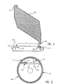
  • FIG. 2 is an end view of the preferred embodiment roller 110 with the preferred embodiment pad 100 held firmly in place.
  • the roller has clamping means 112 disposed at opposite ends, for securely holding the cleaning pad 100 in place on the roller 110 and further includes driving means 114 for rotatably driving the roller.
  • the clamping means 112 on the preferred embodiment roller 110 is a lever 116 mounted in a notch 118.
  • the notch 118 forms a shelf 120 on which the lever 116 is mounted.
  • the lever 116 clamps a pad tab 102 to the shelf 120, firmly holding the clamped tab 102 in place.
  • the preferred lever 116 has a pivot 122 at one end and a serrated surface 124 for gripping the tab 102 at an opposite end.
  • a clamping screw 126 locks the lever 116 firmly against the tab 102, which is thus clamped between the serrated surface 124 and the shelf 120.
  • the clamping screw 126 passes through the lever 116 between the pivot 122 and the serrated surface 124 and enters the roller 110 in a threaded hole 128 in the shelf 120. So, screwing the clamping screw 126 into the shelf 120 tightens the grip of the clamping means 112 on the clamped tab 102.
  • the pad 100 is attached to the roller 110 by inserting one tab 102 into one of the clamping means 112; tightening the clamping screw 126 to clamp the inserted tab 102; wrapping the pad 100 in the intended direction of rotation in a helix-like fashion around the roller 110; and, in FIG. 3B, inserting and clamping the remaining tab 102 in the remaining clamping means 112.
  • the pad edges 130, 132 do not overlap and are gapped from each other.
  • the gap 134 channels used cleaning solution, debris, etc. away and off of the article being cleaned.
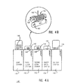
  • FIG. 4B which is an expanded view of the first cleaning station 146 and is typical for both cleaning stations 150 and 152
  • cleaning solution 160 drops onto the cleaning pad and roller assembly 142.
  • the wafer 146' being cleaned passes between a support roller 162 and the cleaning pad/roller assembly 142.
  • the cleaning pad/roller assembly 142 acts to provide fresh cleaning solution to the wafer 146', while simultaneously removing spent, contaminated cleaning solution and debris.
Landscapes

  • Cleaning Or Drying Semiconductors (AREA)
  • Cleaning In General (AREA)
  • Coating Apparatus (AREA)

Abstract

A cleaning pad and roller assembly for cleaning semiconductor wafers. The pad may be a felt sheet with a pair of tabs located at opposite ends. The roller may be polyvinylchloride and may have a drive gear at one end and a clamp at each end. Each clamp is a clamping lever mounted on a shelf and may be locked in place by a clamping screw. Each clamping lever may have a pivot at one end and a serrated surface at an opposite end. The clamping screw may pass through the clamping lever into the shelf.

Description

The present invention relates generally to a pad a roller assembly, and more particularly to a pad and roller assembly suitable for cleaning semiconductor wafers in semiconductor manufacturing apparatus.
Semiconductor chip manufacturing is a complicated multistep process. At each step, a semiconductor wafer may be subjected to some type of chemical process that changes the wafer's structure. Residue or debris may be left on the wafer from a particular chemical process. That residue must be cleaned from the wafer without damaging the partially completed chip structures. One way these wafers are cleaned is washing, i.e., applying a fluid onto the wafer, and then wiping the fluid off with a cleaning pad.
Typical prior art rollers used for cleaning semiconductor wafers include some type of metallic material. However, metals corrode, and corrosion diminishes the pad's cleaning effectiveness. Also, the metal from the roller dissolves, slightly, introducing metallic ions into the cleaning process. These metallic ions may contaminate the wafer rather than cleaning it.
Other types of foreign material from the pad may also contaminate the wafer or circuit, defeating the purpose of cleaning. One source of contamination is the means of attaching the pad to the cleaning apparatus. Some prior art cleaning pads are permanently attached to a roll for easy assembly/disassembly. Typically, they are attached to the roll with glue or metal staples. However, glue may melt, mixing with and contaminating the cleaning solutions. Staples may corrode, providing another source of corrosion. Additionally, staples may project above the pad surface, to scratch the wafer surface being cleaned.
Accordingly, the present invention provides a cleaning pad and roller assembly for cleaning semiconductor wafers comprising a roller and a pad, said pad being clamped at either end and wrapped around said roller in helix-like fashion.
In the preferred embodiment, the roller comprises clamping means at each end for clamping said pad, and driving means for rotatably driving said roller means, wherein the clamping means comprises a notch in a roller end, said notch forming a shelf; a clamping lever mounted in said notch; and locking means for locking said clamping lever in place against said shelf, whereby said pad is clamped by said clamping lever to said shelf. The clamping lever includes a pivot at one end of said clamping lever and a serrated surface at an opposite end of said clamping lever, and the locking means comprises a screw passing through said lever entering said roller, whereby said screw holds said clamping means in place. The roller is polyvinylchloride and the pad is a felt sheet with a pair of tabs at opposing ends. Preferably the pad is 0.035" ± .015" (0.889 ± 0.381 mm) thick.
The invention also provides a cleaning pad and roller assembly for cleaning semiconductor wafers comprising: a felt pad (preferably approximately 0.035" (0.889 mm) thick), with a pair of tabs located at opposite ends of said pad; a polyvinylchloride roller with a drive gear at one end; and a clamp at each end of said roller, each said clamp comprising a clamping lever mounted on a shelf and locked in place by a clamping screw, each said clamping lever having a pivot at one end, and a serrated surface at an opposite end, said clamping screw passing through said clamping lever into said shelf.
Such a cleaning roller and pad may be used in apparatus for cleaning semiconductor wafers in semiconductor chip manufacture, to improve semiconductor wafer cleaning pad effectiveness, without impairing the function of any circuit being cleaned by the pad, and to simplify semiconductor wafer cleaning pad replacement.
The preferred embodiment of the invention has a cleaning pad and roller assembly for cleaning semiconductor wafers, wherein the roller may be polyvinylchloride, and the pad may be a commercially available felt material with a pair of tabs located at opposite ends. The roller may have a drive gear at one end and a clamp at each end. Each clamp is typically a clamping lever mounted on a shelf and may be locked in place by a clamping screw. Each clamping lever may have a pivot at one end and a serrated surface at an opposite end. The clamping screw may pass through the clamping lever into the shelf.
A preferred embodiment of the invention will now be described in detail by way of example only with reference to the following drawings:
  • FIG. 1 is a drawing of a preferred embodiment of a cleaning pad and roller;
  • FIG. 2 is an end view of the preferred embodiment roller and pad, with the cleaning pad in place.
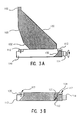
  • FIGS. 3A-B represent the pad being attached to the roller in the preferred embodiment; and
  • FIGS. 4A-B represent the preferred embodiment pad and roller assembly used in a wafer cleaning system.
  • FIG. 1 is a drawing of the preferred cleaning pad 100 and roller 110. The pad 100 is a sheet of felt, preferably 0.035" ± .015" thick (0.889 ± 0.381 mm). The pad 100 has a pair of tabs 102 at opposing ends for attachment to a roller. The pad is shaped such that when in place on the roller, the pad does not overlay itself and does not extend beyond the sides of the roller.
    FIG. 2 is an end view of the preferred embodiment roller 110 with the preferred embodiment pad 100 held firmly in place. The roller has clamping means 112 disposed at opposite ends, for securely holding the cleaning pad 100 in place on the roller 110 and further includes driving means 114 for rotatably driving the roller.
    The clamping means 112 on the preferred embodiment roller 110 is a lever 116 mounted in a notch 118. The notch 118 forms a shelf 120 on which the lever 116 is mounted. The lever 116 clamps a pad tab 102 to the shelf 120, firmly holding the clamped tab 102 in place. The preferred lever 116 has a pivot 122 at one end and a serrated surface 124 for gripping the tab 102 at an opposite end. A clamping screw 126 locks the lever 116 firmly against the tab 102, which is thus clamped between the serrated surface 124 and the shelf 120. Preferably, the clamping screw 126 passes through the lever 116 between the pivot 122 and the serrated surface 124 and enters the roller 110 in a threaded hole 128 in the shelf 120. So, screwing the clamping screw 126 into the shelf 120 tightens the grip of the clamping means 112 on the clamped tab 102.
    In FIG. 3A, the pad 100 is attached to the roller 110 by inserting one tab 102 into one of the clamping means 112; tightening the clamping screw 126 to clamp the inserted tab 102; wrapping the pad 100 in the intended direction of rotation in a helix-like fashion around the roller 110; and, in FIG. 3B, inserting and clamping the remaining tab 102 in the remaining clamping means 112. Once the pad 100 is in place, the pad edges 130, 132 do not overlap and are gapped from each other. When the roller rotates during cleaning, the gap 134 channels used cleaning solution, debris, etc. away and off of the article being cleaned.
    FIG. 4A represents a wafer cleaning apparatus 140 including preferred embodiment cleaning pad and roller assemblies 142, 144. Uncleaned wafers 146 are loaded into loading station 148 which sequentially passes them, one at a time, to a first cleaning station 150. After being partially cleaned in the first cleaning station 150, the partially clean wafer 146' is passed to a second cleaning station 152. From the second cleaning station 152, the cleaned wafer 146" is passed to a rinser/dryer station 154 where the wafer is rinsed and then dried. Finally, the clean, dry wafer 156 is passed to unloading station 158 where it is stored for removal.
    As is apparent from FIG. 4B, which is an expanded view of the first cleaning station 146 and is typical for both cleaning stations 150 and 152, cleaning solution 160 drops onto the cleaning pad and roller assembly 142. The wafer 146' being cleaned passes between a support roller 162 and the cleaning pad/roller assembly 142. The cleaning pad/roller assembly 142 acts to provide fresh cleaning solution to the wafer 146', while simultaneously removing spent, contaminated cleaning solution and debris.
    Claims (9)

    1. A cleaning pad and roller assembly for cleaning semiconductor wafers comprising a roller and a pad, said pad being clamped at either end and wrapped around said roller in helix-like fashion.
    2. The assembly of Claim 1 wherein the roller comprises clamping means at each end for clamping said pad, and driving means for rotatably driving said roller means.
    3. The assembly of Claim 2 wherein the clamping means comprises a notch in a roller end, said notch forming a shelf; a clamping lever mounted in said notch; and locking means for locking said clamping lever in place against said shelf, whereby said pad is clamped by said clamping lever to said shelf.
    4. The assembly of Claim 3 wherein the clamping lever includes a pivot at one end of said clamping lever and a serrated surface at an opposite end of said clamping lever.
    5. The assembly of Claim 4 wherein the locking means comprises a screw passing through said lever entering said roller, whereby said screw holds said clamping means in place.
    6. The assembly of any preceding claim wherein the roller is polyvinylchloride and the pad is a felt sheet with a pair of tabs at opposing ends.
    7. The assembly of any preceding claim wherein the pad is 0.035" ± .015" (0.889 ± 0.381 mm) thick.
    8. A cleaning pad and roller assembly for cleaning semiconductor wafers comprising:
      a felt pad with a pair of tabs located at opposite ends of said pad;
      a polyvinylchloride roller with a drive gear at one end; and
      a clamp at each end of said roller, each said clamp comprising a clamping lever mounted on a shelf and locked in place by a clamping screw, each said clamping lever having a pivot at one end, and a serrated surface at an opposite end, said clamping screw passing through said clamping lever into said shelf.
    9. The assembly of Claim 8 wherein the felt pad is approximately 0.035" (0.889 mm) thick.
    EP97304741A 1996-07-24 1997-07-01 A pad and roller assembly Withdrawn EP0821402A3 (en)

    Applications Claiming Priority (2)

    Application Number Priority Date Filing Date Title
    US686048 1996-07-24
    US08/686,048 US5813082A (en) 1996-07-24 1996-07-24 Pad and roller assembly for cleaning semiconductor wafers

    Publications (2)

    Publication Number Publication Date
    EP0821402A2 true EP0821402A2 (en) 1998-01-28
    EP0821402A3 EP0821402A3 (en) 2002-05-22

    Family

    ID=24754688

    Family Applications (1)

    Application Number Title Priority Date Filing Date
    EP97304741A Withdrawn EP0821402A3 (en) 1996-07-24 1997-07-01 A pad and roller assembly

    Country Status (3)

    Country Link
    US (2) US5813082A (en)
    EP (1) EP0821402A3 (en)
    JP (1) JP3105827B2 (en)

    Cited By (1)

    * Cited by examiner, † Cited by third party
    Publication number Priority date Publication date Assignee Title
    EP0993023A1 (en) * 1998-10-05 2000-04-12 Agfa-Gevaert N.V. Method for transferring a web-or sheet-like material into a clean room

    Families Citing this family (6)

    * Cited by examiner, † Cited by third party
    Publication number Priority date Publication date Assignee Title
    WO1996042100A1 (en) 1995-06-09 1996-12-27 Kabushiki Kaisha Toshiba Impregnated cathode structure, cathode substrate used for the structure, electron gun structure using the cathode structure, and electron tube
    US5813082A (en) * 1996-07-24 1998-09-29 International Business Machines Corporation Pad and roller assembly for cleaning semiconductor wafers
    IL123707A (en) * 1997-05-26 2001-01-28 Heidelberger Druckmasch Ag Method and device for eliminating peeled-off surface portions of an ink-repellent layer of an offset printing plate
    US6951044B2 (en) 2002-02-09 2005-10-04 Kaim Wayne K Paper cleaning buff
    US7481829B2 (en) * 2003-04-21 2009-01-27 Atlas Spine, Inc. Bone fixation plate
    US6920796B2 (en) * 2003-11-13 2005-07-26 Nan Ya Technology Corporation Device used for detecting clamping force of processed object and method thereof

    Family Cites Families (12)

    * Cited by examiner, † Cited by third party
    Publication number Priority date Publication date Assignee Title
    US801003A (en) * 1903-12-21 1905-10-03 United Shoe Machinery Ab Buffing or polishing roll.
    US869572A (en) * 1906-08-04 1907-10-29 James H Hunt Covering for mangle-rolls.
    US2630657A (en) * 1950-12-29 1953-03-10 Earle L Harley Strip material and means for applying same to rollers
    US3234694A (en) * 1963-11-06 1966-02-15 John F Vosburg Abrasive strip holding and tightening mechanism
    US3610693A (en) * 1969-12-30 1971-10-05 Xerox Corp Method of making a cylindrical brush
    US3886622A (en) * 1973-01-26 1975-06-03 Western Sales & Supply Co Tubular buffer element
    JPS58182234A (en) * 1982-04-17 1983-10-25 Dainippon Screen Mfg Co Ltd Washing apparatus allowing use of plural kinds of brushes
    ES283921Y (en) * 1985-01-11 1986-06-16 Alvarez Garcia Jaime PERFECTED DEVICE FOR HELICAL COILING OF TISSUE TAPE ON PLASTIC TUBES FOR PAINT ROLLERS
    US4627127A (en) * 1985-02-13 1986-12-09 Minnesota Mining And Manufacturing Company Cylindrical brush
    US4947029A (en) * 1985-11-01 1990-08-07 Canon Kabushiki Kaisha Cleaning device for information recording medium
    GB8907969D0 (en) * 1989-04-08 1989-05-24 Holdsworth James & Brothers Card clothing
    US5813082A (en) * 1996-07-24 1998-09-29 International Business Machines Corporation Pad and roller assembly for cleaning semiconductor wafers

    Cited By (1)

    * Cited by examiner, † Cited by third party
    Publication number Priority date Publication date Assignee Title
    EP0993023A1 (en) * 1998-10-05 2000-04-12 Agfa-Gevaert N.V. Method for transferring a web-or sheet-like material into a clean room

    Also Published As

    Publication number Publication date
    JPH1083979A (en) 1998-03-31
    EP0821402A3 (en) 2002-05-22
    JP3105827B2 (en) 2000-11-06
    US5813082A (en) 1998-09-29
    US6125496A (en) 2000-10-03

    Similar Documents

    Publication Publication Date Title
    US5813082A (en) Pad and roller assembly for cleaning semiconductor wafers
    EP1661731A3 (en) Process for removing residues from a semiconductor substrate
    EP1077474A2 (en) Backside etching in a scrubber
    JP3626610B2 (en) Processing apparatus and processing method
    JP2930580B1 (en) Cleaning equipment for semiconductor wafers
    US6361614B1 (en) Dark spin rinse/dry
    JPS63133534A (en) Cleaning of semiconductor wafer
    JP3194592B2 (en) Single wafer cleaning equipment
    JP2004063201A (en) Substrate processing equipment
    JPH05160104A (en) Wet processing method and wet processing apparatus for semiconductor wafer
    KR100202670B1 (en) Plating method of semiconductor lead frame
    JPH09199462A (en) Wafer cleaning method and apparatus therefor
    KR20020063201A (en) Method of cleaning electronic device
    JPS5840837A (en) Clamping device
    KR100502406B1 (en) UV tape removal device and method for semiconductor device manufacturing
    CN101312114B (en) Method for Preventing Silicon Wafer Backside from Contaminating Front Side in Immersion Wet Process
    JPH09266188A (en) Surface cleaning method
    KR100583633B1 (en) Substrate Transfer Robot
    JPH08316184A (en) Cleaning method
    JP3716456B2 (en) Etching part manufacturing method
    JP2879007B2 (en) Processing equipment
    JPH09260328A (en) Silicon wafer surface treatment method
    JPS62185327A (en) Treatment device
    KR20070068902A (en) Device that can remove the contamination on the back of the photo mask with pellicle attached
    JPH0845889A (en) Cleaning equipment

    Legal Events

    Date Code Title Description
    PUAI Public reference made under article 153(3) epc to a published international application that has entered the european phase

    Free format text: ORIGINAL CODE: 0009012

    AK Designated contracting states

    Kind code of ref document: A2

    Designated state(s): AT BE CH DE DK ES FI FR GB GR IE IT LI LU MC NL PT SE

    PUAL Search report despatched

    Free format text: ORIGINAL CODE: 0009013

    RIC1 Information provided on ipc code assigned before grant

    Free format text: 7H 01L 21/00 A, 7B 08B 11/00 B, 7B 08B 1/04 B, 7A 46B 13/00 B

    AKX Designation fees paid
    REG Reference to a national code

    Ref country code: DE

    Ref legal event code: 8566

    STAA Information on the status of an ep patent application or granted ep patent

    Free format text: STATUS: THE APPLICATION IS DEEMED TO BE WITHDRAWN

    18D Application deemed to be withdrawn

    Effective date: 20021123