EP0821448A2 - Assemblement pour carte de circuit imprimé et sa méthode d'assemblage - Google Patents
Assemblement pour carte de circuit imprimé et sa méthode d'assemblage Download PDFInfo
- Publication number
- EP0821448A2 EP0821448A2 EP97112579A EP97112579A EP0821448A2 EP 0821448 A2 EP0821448 A2 EP 0821448A2 EP 97112579 A EP97112579 A EP 97112579A EP 97112579 A EP97112579 A EP 97112579A EP 0821448 A2 EP0821448 A2 EP 0821448A2
- Authority
- EP
- European Patent Office
- Prior art keywords
- circuit board
- card connector
- solder tails
- printed circuit
- soldering
- Prior art date
- Legal status (The legal status is an assumption and is not a legal conclusion. Google has not performed a legal analysis and makes no representation as to the accuracy of the status listed.)
- Withdrawn
Links
Images

Classifications
-
- H—ELECTRICITY
- H01—ELECTRIC ELEMENTS
- H01R—ELECTRICALLY-CONDUCTIVE CONNECTIONS; STRUCTURAL ASSOCIATIONS OF A PLURALITY OF MUTUALLY-INSULATED ELECTRICAL CONNECTING ELEMENTS; COUPLING DEVICES; CURRENT COLLECTORS
- H01R43/00—Apparatus or processes specially adapted for manufacturing, assembling, maintaining, or repairing of line connectors or current collectors or for joining electric conductors
- H01R43/20—Apparatus or processes specially adapted for manufacturing, assembling, maintaining, or repairing of line connectors or current collectors or for joining electric conductors for assembling or disassembling contact members with insulating base, case or sleeve
- H01R43/205—Apparatus or processes specially adapted for manufacturing, assembling, maintaining, or repairing of line connectors or current collectors or for joining electric conductors for assembling or disassembling contact members with insulating base, case or sleeve with a panel or printed circuit board
-
- H—ELECTRICITY
- H01—ELECTRIC ELEMENTS
- H01R—ELECTRICALLY-CONDUCTIVE CONNECTIONS; STRUCTURAL ASSOCIATIONS OF A PLURALITY OF MUTUALLY-INSULATED ELECTRICAL CONNECTING ELEMENTS; COUPLING DEVICES; CURRENT COLLECTORS
- H01R12/00—Structural associations of a plurality of mutually-insulated electrical connecting elements, specially adapted for printed circuits, e.g. printed circuit boards [PCB], flat or ribbon cables, or like generally planar structures, e.g. terminal strips, terminal blocks; Coupling devices specially adapted for printed circuits, flat or ribbon cables, or like generally planar structures; Terminals specially adapted for contact with, or insertion into, printed circuits, flat or ribbon cables, or like generally planar structures
- H01R12/70—Coupling devices
- H01R12/71—Coupling devices for rigid printing circuits or like structures
- H01R12/712—Coupling devices for rigid printing circuits or like structures co-operating with the surface of the printed circuit or with a coupling device exclusively provided on the surface of the printed circuit
- H01R12/716—Coupling device provided on the PCB
Definitions
- the present invention relates to a PC card connector assembly and a method of assembling a PC card connector assembly comprising a printed circuit board and a PC card connector on each side of the printed circuit board, each PC card connector having signal terminals and ground terminals.
- solder tails formed in a right angle configuration and positioned at the rear end of the PC card connector such that the ends of the solder tails are directed to and in contact with circuit traces on the underlying printed circuit board.
- solder tails are often fixed to the circuit board by dip-soldering whereby they are inserted in through-holes made in the circuit board and then soldered.
- the circuit board uses a relatively large area allotted to the layout of the through-holes for accommodating each row of solder tails (often two rows of tails for the signal terminals and one for the ground terminals) for each connector.
- solder tails often two rows of tails for the signal terminals and one for the ground terminals
- One attempt to solve the problem of occupying such a large area with through-holes is to place one PC card connector on one side of the circuit board and a second PC card connector on the other side of the circuit board. In assembling such an arrangement, however, there are some tradeoffs due to the layout that must be considered.
- solder tails of the signal and ground terminals are arranged in at least two different rows, alignment of the solder tails with respect to the circuit pattern formed on the circuit board is difficult to inspect and correct. Particularly, visually inspecting and correcting the alignment of the solder tails positioned toward the inside of the assembly is more difficult than inspecting and correcting the solder tails positioned toward the outside of the assembly.
- One object of the present invention is to provide a dual port PC connector assembly occupying a relatively small area on the printed circuit board, while allowing and facilitating visual inspection and correction of the alignment of the solder tails of the signal and ground terminals.
- a PC card connector assembly is improved according to the present invention in that it comprises: a first PC card connector for mounting to a printed circuit board including signal terminals having surface mount solder tails adapted to be surface mounted to a first side of the circuit board; a first ground piece mounted on the first PC card connector and including through-hole solder tails adapted to be mounted within holes in the circuit board; a second PC card connector for mounting to the circuit board including signal terminals having surface mount solder tails adapted to be surface mounted to an opposite side of the circuit board; and a second ground piece for mounting on the second PC card connector and including surface mount solder tails adapted to be mounted to the surface of the opposite side of the circuit board.
- a method of forming a PC card connector assembly comprising the steps of: attaching the first PC card connector to one side of the printed circuit board, the solder tails of the signal terminals of the first PC card connector being of surface mount type, and the solder tails of the ground piece of the first PC card connector being of dip-soldering type; soldering the solder tails of the signal terminals of the first PC card connector to the signal circuit pattern formed on the surface of the one side of the circuit board; soldering the solder tails of the ground piece of the first PC card connector within the through-holes of a ground circuit of the printed circuit board; attaching the second PC card connector to an opposite side of the circuit board, the solder tails of the signal terminals of the second PC card connector being of surface mount type; soldering the solder tail
- Soldering the solder tails of the signal terminals and soldering the solder tails of the ground piece of the first PC card connector on the first side of the circuit board can be effected simultaneously by reflow soldering, for example.
- the surface mount solder tails of the signal and ground terminals of the second PC card connector are soldered to the circuit pattern formed on the opposite side of the circuit board, thus reducing the total area occupied on the circuit board by the dual port PC card assembly.
- visual inspection of the solder tails of the signal terminals of the first PC connector can be performed without obstruction by the solder tails of the ground terminals.
- the solder tails of the ground terminals can also be inspected from the opposite side without obstruction.
- Visual inspection of the solder tails of the signal terminals of the second PC connector can be performed without obstruction by the solder tails of the ground terminals, which are soldered subsequent to the signal terminals.
- the solder tails of the ground terminals can also be inspected easily, i.e., without visual obstruction, after it is assembled on the second PC card connector.
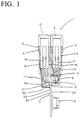
- a PC card connector assembly 1 comprises a printed circuit board 2 and first and second PC card connectors 3 and 4 fixed to front and rear sides 2a and 2b of printed circuit board 2, respectively.
- Printed circuit board 2 has a receptacle connector 5 for connecting the printed circuit board to a group of wires or other electrical boards via an associated plug connector (not shown).
- PC card connector 3 mounted on the front side of the printed circuit board includes right angle-configured signal terminals 8 which have two rows of contacts 7 located in a card slot 6 of a connector housing 10 of PC card connector 3.
- Surface mount solder tails 11 of signal terminals 8 are adapted to be surface mounted to a conductive pattern 12 of a signal circuit (not shown) formed on the surface of front side 2a of printed circuit board 2.
- the connector housing 10 has a ground terminal piece 9 mounted thereto.
- Right angle-configured solder tails 13 of ground piece 9 are adapted to be dip-soldered within through-holes 14 of a ground circuit (not shown) on front side 2a of circuit board 2.
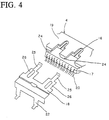
- PC card connector 4 mounted on rear side 2b of printed circuit board 2 includes right angle-configured signal terminals 17 which have two rows of contacts 16 located in a card slot 15 of a connector housing 19.
- Surface mount solder tails 20 of signal terminals 17 are adapted to be surface-mounted to a conductive pattern 21 of a signal circuit formed on the surface of rear side 2b of circuit board 2.
- Connector housing 19 has a ground terminal piece 18 mounted thereon.
- Ground piece 18 comprises a lateral base, mount projections 26 integrally connected to one side of the lateral base, each projection having a contact 25 integrally connected thereto, and right angle-configured solder tails 22 integrally connected to the other side of the lateral base.
- Connector housing 19 has insertion slots with notched edges 24 in opposite sides of the slots, thus permitting the insertion of mount projections 26 of ground piece 18 into connector housing 19.
- Surface mount solder tails 22 of ground terminal piece 18 are adapted to be surface mounted to a conductive pattern 23 of a ground circuit (not shown) also formed on the surface of rear side 2b of circuit board 2.
- the method comprises the steps of: placing the first PC card connector 3 on a first side 2a of the printed circuit board 2, inserting the through-hole solder tails 13 of ground piece 9 in the through-holes 14 of the circuit board, and placing the surface mount solder tails 11 of the signal terminals 8 on the conductive pattern 12 formed on the surface of first side 2a of the circuit board.
- the soldering of both sets of solder tails can be effected simultaneously, for example by reflow soldering.
- the location and alignment of the surface mount solder tails 11 relative to the conductive pattern 12 is visually inspected so that misalignments and other problems with the solder tails can be detected and corrected before soldering.
- a second PC connector 4 is placed on the second or opposite side 2b of the circuit board, and the required solder connections are made.
- the second PC connector 4 is designed to permit the subsequent assembly of separate ground piece 18 to the connector housing 19.
- the alignment of surface mount solder tails 20 of signal terminals 17 relative to a conductive pattern 21 formed on the surface of the second side of the circuit board is visually inspected, and misalignments and other problems with the signal terminal solder tails 20 can be detected and corrected.
- the inspection and correction of misalignments of the solder tails can be performed without difficulty because there are no obstacles that interfere.
- the solder tails are soldered to the conductive pattern 21, for example by reflow soldering. After soldering, visual inspection of the solder joint can also be made.
- the ground piece 18 is press-fit into the connector housing 19 of the second PC card connector so that solder tails 22 of the ground piece are in contact with the corresponding portions of a conductive pattern 23 of a ground circuit formed on the second side of the circuit board.
- Visual inspection of the relative positioning between solder tails 22 and the corresponding portions of conductive pattern 23 of the ground circuit can be made easily because the interface is visually free of any obstacles.
- the tails are soldered to the ground circuit. After soldering, the solder joints can be inspected as well.
Landscapes
- Engineering & Computer Science (AREA)
- Manufacturing & Machinery (AREA)
- Coupling Device And Connection With Printed Circuit (AREA)
- Details Of Connecting Devices For Male And Female Coupling (AREA)
- Manufacturing Of Electrical Connectors (AREA)
- Multi-Conductor Connections (AREA)
Applications Claiming Priority (2)
| Application Number | Priority Date | Filing Date | Title |
|---|---|---|---|
| JP8215531A JP3066570B2 (ja) | 1996-07-26 | 1996-07-26 | Pcカード用コネクタアッセンブリの製造方法 |
| JP215531/96 | 1996-07-26 |
Publications (2)
| Publication Number | Publication Date |
|---|---|
| EP0821448A2 true EP0821448A2 (fr) | 1998-01-28 |
| EP0821448A3 EP0821448A3 (fr) | 1999-03-03 |
Family
ID=16673978
Family Applications (1)
| Application Number | Title | Priority Date | Filing Date |
|---|---|---|---|
| EP97112579A Withdrawn EP0821448A3 (fr) | 1996-07-26 | 1997-07-23 | Assemblement pour carte de circuit imprimé et sa méthode d'assemblage |
Country Status (6)
| Country | Link |
|---|---|
| US (1) | US5964597A (fr) |
| EP (1) | EP0821448A3 (fr) |
| JP (1) | JP3066570B2 (fr) |
| MY (1) | MY122003A (fr) |
| SG (1) | SG67407A1 (fr) |
| TW (1) | TW460101U (fr) |
Families Citing this family (11)
| Publication number | Priority date | Publication date | Assignee | Title |
|---|---|---|---|---|
| MY123239A (en) | 1998-12-18 | 2006-05-31 | Molex Inc | Card-receiving connector with grounding terminal |
| TW415706U (en) * | 1999-05-15 | 2000-12-11 | Hon Hai Prec Ind Co Ltd | Electronic card connector device |
| US6978335B2 (en) * | 2000-06-30 | 2005-12-20 | 02Micro International Limited | Smart card virtual hub |
| US7000249B2 (en) * | 2001-05-18 | 2006-02-14 | 02Micro | Pre-boot authentication system |
| US7797729B2 (en) * | 2000-10-26 | 2010-09-14 | O2Micro International Ltd. | Pre-boot authentication system |
| US6459602B1 (en) | 2000-10-26 | 2002-10-01 | O2 Micro International Limited | DC-to-DC converter with improved transient response |
| US20030013414A1 (en) * | 2001-07-13 | 2003-01-16 | Huang Yishao Max | Radio system for providing wireless connectivity between digital devices |
| US6913196B2 (en) * | 2002-02-20 | 2005-07-05 | O2Micro International Limited | Dual mode controller for ISO7816 and USB enabled smart cards |
| TWM243815U (en) * | 2003-10-14 | 2004-09-11 | Molex Taiwan Ltd | Electronic card connector |
| TW200824192A (en) * | 2006-11-24 | 2008-06-01 | Fci Connectors Singapore Pte | Electric connector |
| FR2971095B1 (fr) * | 2011-02-01 | 2013-11-08 | Tyco Electronics France Sas | Connecteur electrique pour systeme de retenue de securite comportant une borne de mise a la terre |
Family Cites Families (12)
| Publication number | Priority date | Publication date | Assignee | Title |
|---|---|---|---|---|
| US4871321A (en) * | 1988-03-22 | 1989-10-03 | Teradyne, Inc. | Electrical connector |
| DE69018000T2 (de) | 1989-10-10 | 1995-09-28 | Whitaker Corp | Rückwandsteckverbinder mit angepasster Impedanz. |
| US5299089A (en) * | 1991-10-28 | 1994-03-29 | E. I. Dupont De Nemours & Co. | Connector device having two storage decks and three contact arrays for one hard disk drive package or two memory cards |
| US5308251A (en) * | 1992-08-10 | 1994-05-03 | The Whitaker Corporation | Mounting bracket with ESD protection for an electrical connector |
| US5305182A (en) * | 1992-10-14 | 1994-04-19 | Chen Teng Ka | Read/write unit for two integrated circuit cards |
| NL9202302A (nl) * | 1992-12-31 | 1994-07-18 | Du Pont Nederland | Koaxiaal interkonnektiesysteem. |
| JP2567629Y2 (ja) * | 1993-03-23 | 1998-04-02 | バーグ・テクノロジー・インコーポレーテッド | コネクタ装置 |
| US5316488A (en) * | 1993-06-04 | 1994-05-31 | Molex Incorporated | Connector apparatus for IC packs |
| US5399105A (en) * | 1994-04-29 | 1995-03-21 | The Whitaker Corporation | Conductive shroud for electrical connectors |
| US5478260A (en) * | 1994-07-29 | 1995-12-26 | The Whitaker Corporation | Grounding for electrical connectors |
| US5470259A (en) * | 1994-12-05 | 1995-11-28 | The Whitaker Corporation | Grounding shroud for surface mounted electrical connector |
| DE29601655U1 (de) * | 1996-01-31 | 1996-03-28 | Siemens AG, 80333 München | Baugruppenleiterplatte mit Steckverbinder |
-
1996
- 1996-07-26 JP JP8215531A patent/JP3066570B2/ja not_active Expired - Fee Related
-
1997
- 1997-07-16 US US08/895,144 patent/US5964597A/en not_active Expired - Fee Related
- 1997-07-23 EP EP97112579A patent/EP0821448A3/fr not_active Withdrawn
- 1997-07-23 SG SG1997002612A patent/SG67407A1/en unknown
- 1997-07-25 MY MYPI97003409A patent/MY122003A/en unknown
- 1997-07-29 TW TW087211501U patent/TW460101U/zh not_active IP Right Cessation
Also Published As
| Publication number | Publication date |
|---|---|
| US5964597A (en) | 1999-10-12 |
| JP3066570B2 (ja) | 2000-07-17 |
| JPH1040982A (ja) | 1998-02-13 |
| SG67407A1 (en) | 1999-09-21 |
| TW460101U (en) | 2001-10-11 |
| EP0821448A3 (fr) | 1999-03-03 |
| MY122003A (en) | 2006-03-31 |
Similar Documents
| Publication | Publication Date | Title |
|---|---|---|
| US6315620B1 (en) | System, method, and device for a pre-loaded straddle mounted connector assembly | |
| CN101180769B (zh) | 板对板连接器 | |
| US6527588B2 (en) | Electrical connector with integrated PCB assembly | |
| JPH08124637A (ja) | 表面実装型電気コネクタ | |
| US6863572B1 (en) | Electrical connector with shock support | |
| US5310354A (en) | Integral ground terminal and tail shield | |
| KR100297956B1 (ko) | 신호단자 및 접지단자를 갖는 커넥터조립체 | |
| US6176743B1 (en) | Electrical adapter | |
| EP0661779A1 (fr) | Dispositif de connecteurs multiples | |
| US5964597A (en) | PC card assembly and method of assembling the same | |
| US5997312A (en) | Grounding contact for high speed, high density connector | |
| US5709555A (en) | High density card edge connection system with outrigger and sequentially connected contacts | |
| US6135784A (en) | LIF PGA socket | |
| US6095824A (en) | Electrical connector assembly | |
| US6322392B1 (en) | Ground plate structure for a PC card connector assembly | |
| TW200403888A (en) | Board mounted electrical connector with improved ground terminals | |
| EP0245161A1 (fr) | Structure pour fixation de queues de broches de connecteurs électriques | |
| EP0643448B1 (fr) | Connecteur coaxial pour la connexion de plaquettes de circuits imprimés | |
| US6152765A (en) | Electrical connector | |
| US20120178299A1 (en) | Surface-mount on-board diagnostics connector-pin assembly | |
| EP0499436B1 (fr) | Hameçon poussoir | |
| US6736647B1 (en) | Printed circuit board connector | |
| US20100221930A1 (en) | Plug device, plug connector, and method for producing the plug connector | |
| US6949989B2 (en) | Electronic signal filter including solderless ground clip having surge protection and shielding features | |
| JP3715720B2 (ja) | Icカード用コネクタ |
Legal Events
| Date | Code | Title | Description |
|---|---|---|---|
| PUAI | Public reference made under article 153(3) epc to a published international application that has entered the european phase |
Free format text: ORIGINAL CODE: 0009012 |
|
| AK | Designated contracting states |
Kind code of ref document: A2 Designated state(s): AT BE CH DE DK ES FI FR GB GR IE IT LI LU MC NL PT SE |
|
| PUAL | Search report despatched |
Free format text: ORIGINAL CODE: 0009013 |
|
| AK | Designated contracting states |
Kind code of ref document: A3 Designated state(s): AT BE CH DE DK ES FI FR GB GR IE IT LI LU MC NL PT SE |
|
| AKX | Designation fees paid | ||
| STAA | Information on the status of an ep patent application or granted ep patent |
Free format text: STATUS: THE APPLICATION IS DEEMED TO BE WITHDRAWN |
|
| 18D | Application deemed to be withdrawn |
Effective date: 19990904 |
|
| REG | Reference to a national code |
Ref country code: DE Ref legal event code: 8566 |