EP0821478A2 - Circuit de silencieux électrique - Google Patents
Circuit de silencieux électrique Download PDFInfo
- Publication number
- EP0821478A2 EP0821478A2 EP97112876A EP97112876A EP0821478A2 EP 0821478 A2 EP0821478 A2 EP 0821478A2 EP 97112876 A EP97112876 A EP 97112876A EP 97112876 A EP97112876 A EP 97112876A EP 0821478 A2 EP0821478 A2 EP 0821478A2
- Authority
- EP
- European Patent Office
- Prior art keywords
- mute
- counter
- control
- audio signal
- input
- Prior art date
- Legal status (The legal status is an assumption and is not a legal conclusion. Google has not performed a legal analysis and makes no representation as to the accuracy of the status listed.)
- Granted
Links
- 230000005236 sound signal Effects 0.000 claims abstract description 62
- 238000013016 damping Methods 0.000 claims abstract description 37
- 239000003990 capacitor Substances 0.000 description 10
- 238000000034 method Methods 0.000 description 10
- 230000008569 process Effects 0.000 description 10
- 230000009977 dual effect Effects 0.000 description 5
- 230000008859 change Effects 0.000 description 4
- 238000012545 processing Methods 0.000 description 4
- 230000002238 attenuated effect Effects 0.000 description 2
- 238000010586 diagram Methods 0.000 description 2
- 230000000694 effects Effects 0.000 description 2
- 238000005516 engineering process Methods 0.000 description 2
- 230000008901 benefit Effects 0.000 description 1
- 230000005540 biological transmission Effects 0.000 description 1
- 230000000903 blocking effect Effects 0.000 description 1
- 230000001419 dependent effect Effects 0.000 description 1
- 238000013461 design Methods 0.000 description 1
- 238000007599 discharging Methods 0.000 description 1
- 238000011156 evaluation Methods 0.000 description 1
- 230000006266 hibernation Effects 0.000 description 1
- 230000006872 improvement Effects 0.000 description 1
- 238000004519 manufacturing process Methods 0.000 description 1
- 230000000630 rising effect Effects 0.000 description 1
- 230000029305 taxis Effects 0.000 description 1
- 230000007704 transition Effects 0.000 description 1
- 238000012795 verification Methods 0.000 description 1
Images


Classifications
-
- H—ELECTRICITY
- H04—ELECTRIC COMMUNICATION TECHNIQUE
- H04H—BROADCAST COMMUNICATION
- H04H40/00—Arrangements specially adapted for receiving broadcast information
- H04H40/18—Arrangements characterised by circuits or components specially adapted for receiving
- H04H40/27—Arrangements characterised by circuits or components specially adapted for receiving specially adapted for broadcast systems covered by groups H04H20/53 - H04H20/95
- H04H40/36—Arrangements characterised by circuits or components specially adapted for receiving specially adapted for broadcast systems covered by groups H04H20/53 - H04H20/95 specially adapted for stereophonic broadcast receiving
- H04H40/45—Arrangements characterised by circuits or components specially adapted for receiving specially adapted for broadcast systems covered by groups H04H20/53 - H04H20/95 specially adapted for stereophonic broadcast receiving for FM stereophonic broadcast systems receiving
-
- H—ELECTRICITY
- H03—ELECTRONIC CIRCUITRY
- H03G—CONTROL OF AMPLIFICATION
- H03G3/00—Gain control in amplifiers or frequency changers
- H03G3/20—Automatic control
- H03G3/30—Automatic control in amplifiers having semiconductor devices
- H03G3/34—Muting amplifier when no signal is present
- H03G3/341—Muting when no signals or only weak signals are present
-
- H—ELECTRICITY
- H03—ELECTRONIC CIRCUITRY
- H03H—IMPEDANCE NETWORKS, e.g. RESONANT CIRCUITS; RESONATORS
- H03H11/00—Networks using active elements
- H03H11/02—Multiple-port networks
- H03H11/24—Frequency-independent attenuators
- H03H11/245—Frequency-independent attenuators using field-effect transistor
-
- H—ELECTRICITY
- H04—ELECTRIC COMMUNICATION TECHNIQUE
- H04H—BROADCAST COMMUNICATION
- H04H20/00—Arrangements for broadcast or for distribution combined with broadcast
- H04H20/26—Arrangements for switching distribution systems
-
- H—ELECTRICITY
- H04—ELECTRIC COMMUNICATION TECHNIQUE
- H04H—BROADCAST COMMUNICATION
- H04H2201/00—Aspects of broadcast communication
- H04H2201/10—Aspects of broadcast communication characterised by the type of broadcast system
- H04H2201/13—Aspects of broadcast communication characterised by the type of broadcast system radio data system/radio broadcast data system [RDS/RBDS]
Definitions
- the invention relates to an electrical mute control circuit for soft mute control of an audio signal.
- RDS radio equipment used for processing of RDS signals are able.
- RDS stands for radio Data system and means that from the broadcaster is not audible signals are emitted with, for example to display the name or an abbreviation of the straight received station serve and information about further than the received transmitter frequencies of the received broadcast program contain.
- DE 42 27 680 A1 describes an FM receiver with RDS evaluation known which when receiving an RDS program temporarily on at least one on a first frequency second alternative frequency of the received program for Checking their reception quality switches, the Receiver muted on playback side during verification becomes.
- DE 43 18 667 A1 describes an audio device with an RDS receiver, a CD player and a tape player known, in which case if the reception quality threatens to become too bad, for example in the case of an RDS car radio when approaching a tunnel unpleasant noise is avoided by during the time the reception quality drops below a certain threshold automatically on playback the audio signal from the CD player or the tape player is switched.
- An RDS receiving device is known from DE 43 09 518 A1, where the LF signal with poor reception quality is temporarily steamed. To this end, be ongoing an auxiliary signal dependent on the field strength and a further auxiliary signal derived from the demodulated signal and will these two auxiliary signals form the Quality signal combined. With the one auxiliary signal is evaluated whether there are amplitudes of above 60 kHz Signal components there that are above a threshold lie. The second auxiliary signal is used to evaluate whether the two sidebands of the two-sideband amplitude modulation lie symmetrically to the wearer or not. A Asymmetry in this regard indicates that a there is an audible disturbance.
- a feature of RDS radios is that if the reception quality of the station program just received falls below a certain quality value, automatically to another of those communicated in the RDS signal Receiving frequencies of the same program is switched.
- a conventional mute control circuit for soft Muting an audio signal uses a capacitor which is charged with a predetermined time constant or is discharged, depending on whether you are soft in the Mute state goes or soft the mute state leaves.
- the rising charging voltage or falling discharging voltage the capacitor is used as a damping ramp, by means of which the amplitude of the signal to be attenuated increasingly reduced to zero and when leaving the silent state the amplitude of the signal increasing from zero. This succeeds but only incompletely with reasonable effort. It will almost only the envelope of the signal to be muted accordingly the damping ramp is increasingly reduced or increases, since there is only one in simple circuits Clamping or limiting process results in which the signal to be muted according to the damping ramp is increasingly limited or limited.
- the applicant has a monolithically integrated audio signal processor developed the audio signal processing of a stereo radio in a very wide range carries out. This works for your company Switch to a number of external circuit components back, which are mainly capacitors. Through a variety of measures it is the applicant managed a monolithically integrated circuit for creating audio signal processing that with significant fewer external circuit components get along, with corresponding Saving of connecting pins compared to the conventional integrated circuit. This leads to significant Cost savings, on the one hand, in that for the integrated circuit uses a simpler housing can be, and on the other hand in that a significant Number of external circuit components can be saved can.
- a digitally controllable damping circuit has an audio signal input, an audio signal output and has a control signal input, and the further includes an up / down counter that one Clock pulse input for the supply of to be counted Clock pulses, a counting control input for feeding a counting control signal which controls the counting start and counting stop and a count signal output on which a digital Counter signal is removable and that with the control signal input is connected to the damping circuit.
- variable clock pulse source Use clock frequency For this purpose one can use a variable clock pulse source Use clock frequency. Another possibility is that, several clock pulse sources with different clock frequencies to use and between these clock pulse sources and the clock pulse input of the counter a selector, preferably in the form of an electronic selection switch, to switch, by means of which one certain of the clock pulse sources is selectable.
- mute is used below not just the process of attenuating the audio signal into the silent state but also leading out the Audio signal from the silent state by its growth include from zero.
- mute control circuit are the counter status signal output of the counter and the control signal input of the damping circuit via a data connection for digital transmission of a representing the respective count signal in the dual number system n-digit data word connected to each other, where n is a predetermined integer.
- Each of the switching control devices each of the attenuators is different the n digits of the data word can be supplied as a switching control signal and are the resistance values of the resistors of the individual attenuators different, depending on on the values of the individual attenuators assigned positions of the data word.
- a mute control circuit constructed with such attenuators has the advantage that Hibernation, i.e. outside of the mute processes, no cross currents flow through the damping circuit because in the idle state always all first or all second switches are controlled non-conducting. With this damping circuit thus arises outside the processes of steering into it into the silent state and stepping out the silent state no loss of performance.
- Particularly advantageous for this embodiment is on the one hand that neither resistors capacitors are still required, and on the other hand that the entire mute control circuit is in pure MOS process technology can be produced, i.e. with a relative simple manufacturing technology.
- Each of the MOS switches can be made by a single MOS transistor will be realized. However, preference is given to each of the MOS switches is constructed with a parallel connection, the NMOS transistor having an N channel and has a PMOS transistor having a P-channel, which are always conductive or non-conductive at the same time are switchable, their parallel when switched on on-state resistances to each other Form the resistance of the attenuator. With this embodiment can be a more extensive linearity for reach the resulting switch-on resistance than at the use of only a single MOS transistor per Switch, and this eliminates distortion of the audio signal keep it even smaller.
- Data line connecting the counter and the damping circuit can be designed as a parallel data line with n-bit lines be and the control signal input of the damping circuit can accordingly n control signal connections exhibit.
- the gate electrode can be used for each attenuator of the MOS transistor belonging to the first resistor and the gate electrode of the to the second resistor belonging PMOS transistor directly and the gate electrode of the PMOS transistor belonging to the first resistor and the gate electrode of the one belonging to the second resistor NMOS transistor via an inverter with the associated Control signal connection may be connected, or vice versa.
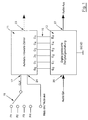
- the mute control circuit shown in Fig. 1 includes one Up / down counter 11 and a digitally controlled Damping circuit 13, which is via a parallel data line 15 are connected to one another, which in the case of FIG. 1 embodiment shown comprises six individual lines.
- the counter 11 has a clock pulse input 17 to which counting clock pulses CLK can be supplied.
- the clock pulse input 17 is optionally available via a selection switch 19 one of several clock pulse sources F1, F2, F3, .... Fm connectable, each having a different clock frequency.
- the counter has a counter control input 21 for controlling the supply of a counting start and counting stop Counter control signal MUTE ON / MUTE OFF.
- the counter 11 has a control signal output 23 at which the Counter 11 at the end of each mute or mute control emits a signal MUTE READY.
- the Counter 11 has a count signal output with n count signal output connections D0, D1, D2, D3, D4 .... Dn open, their number n the number of individual lines of the data line 15 corresponds to.
- the damping circuit 13 has an audio signal input 25, an audio signal output 27, a signal ground connection SGND and a control signal input with n control signal input connections E0, E1, E2, E3, E4, .... En, where n again equal to the number of individual lines of the data line 15 is.
- n 6
- FIG. 2 shows an audio signal AS which occurs at a time t0 has a constant amplitude A1. It is assumed that at this time the clock pulse input 17 of the counter 11 via the selection switch 19 with the clock pulse source F1 is connected.
- the counter control input 21 of the Counter 11 is supplied with a signal MUTE ON, which starts a count of the counter 11 starts, whereupon the counter 11 begins to count the clock pulses supplied to him CLK.
- the total damping factor of the digitally controlled Damping circuit 13 changed step by step, the amplitude of what is passed through the damping circuit 13 Audio signal thus changed step by step.
- the audio signal is minimally attenuated, while with a other predetermined count of the counter maximum is steamed. The begins at time t1 Counter of the minimum signal attenuation or in counts essentially no signal attenuation with the count towards the maximum damping effect Count reached at time t2.
- the audio signal AS is at zero or damped essentially zero, the process of soft Muting ended.
- the counter sends a signal via its control signal output 23 MUTE DONE, which is used for other control can be, for example, one in the mute state trigger switching operation to be performed, for example an RDS frequency hopping.
- Fig. 1 shown mute a feedback of Audio signal AS started to its undamped amplitude A1.
- the counter starts in the opposite direction than to count between times t1 and t2, which is a gradually lower attenuation of the audio signal AS by the damping circuit 13 and thus its stepwise Increase.
- time t4 it is again the minimum damping effect of the counter 11 reached.
- the control signal output 23 of counter 11 again a signal MUTE READY submitted.
- Fig. 3 shows muting operations in which the amplitude attenuation during muting or leading out of the silent state not with constant Amplitude change run but after a predetermined non-linear characteristic. This is achieved in that at predetermined times, the lie between t1 and t2, the selection switch 19 in succession to various of the clock pulse sources F1 to Fm switches so that the counting speed of the counter 11 is changed accordingly. This leads to a corresponding damping change of different speeds Damping circuit 13 and thus to the non-linear Damping curve according to FIG. 3.
- selection switch 19 which is preferably electronic Switch device is designed by means of control a selection program that after triggering a Muting automatically a program-based switchover of the selection switch 19 controls.
- This selection program can be used according to the individual applications shape.
- the MUTE DONE signal can also be used to the counter 11 at the completion of a mute Time t2 or when a process is completed at Exit from mute at time t4 for prepare the other counting direction.
- Another Possibility is when reaching the maximum To generate a count value of the counter 11 an overflow bit, by means of which the switching of the counting direction of the counter 11 is controlled.
- FIG. 4 shows an embodiment of a muting, in which the damping circuit 13 one between the Audio signal input 25 and the audio signal output 27 switched Parallel connection with n attenuators S0, S1, ... Sn.
- Each of these attenuators has a partial voltage tap connected to the audio signal output 27 TA as well as one between the audio signal input 25 and the partial voltage tap TA switched first MOS transistor T1 and one between the partial voltage tap TA and the signal ground connection SGND switched second MOS transistor T2.
- Each of these MOS transistors practically represents the series connection from a switch-on resistor Ron and one through the switching transistor formed electronic switch.
- the gate electrodes from T1 and T2 of the individual attenuators S0 to Sn are each with one of the counter signal output connections D0 to Dn, namely the gate electrode of T1 directly and the gate electrode of T2 via an inverter INV if T1 and T2 are MOS transistors of the same Channel type. Is used for T1 and T2 MOS transistors different channel types, the inverter is INV not mandatory. This will make the two transistors T1 and T2 switched in opposite directions, such that one each switched on and the other is switched off is.
- the turn-on resistors Ron of the transistors T1 and T2 of the individual attenuators S0 to Sn are of different sizes, depending on which dual digit of the data word transmitted via the data line 15 from the counter 11 to the attenuator circuit 13 controls the respective attenuator.
- the weighting is taken with regard to the resistance values of the on-resistances Ron of the attenuators S0 to Sn Ron x 2 n
- the lowest-order switch-on resistance Ron x 1 is assigned to the attenuator Sn assigned to the most significant bit, while in the exemplary embodiment shown with six count signal output connections, an on-resistance resistor Ron x 2 5 is assigned to the attenuator S0 belonging to the least significant bit.
- Deviating from the embodiment shown in FIG. 4 can also use the individual attenuators S0 to Sn component-related resistances and Switches are constructed, each attenuator one between the audio signal input 25 and the partial voltage tap TA switched first series connection with a first resistor and a first controllable Switch and one between the partial voltage tap TA and the signal ground connection SGND connected second series connection with a second resistor and a second controlled switch.
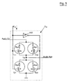
- FIG. 5 shows a further possibility of an attenuator, which is suitable for the damping circuit 13.
- the attenuator Sn is shown and the other attenuators S0 to S4 are constructed identically.
- Attenuator In contrast to the embodiment shown in FIG. 4 of attenuators has the attenuator shown in Fig. 5 between the audio signal input 25 and the audio signal output 27 on the one hand and the audio signal output 27 and the signal ground connection SGND on the other hand each Parallel connection from an NMOS transistor T11 or T22 and a PMOS transistor T12 or T21.
- the on resistors Ron of all four transistors T11, T12, T21 and T22 are the same size.
- the gate electrodes of T11 and T21 are direct and the gate electrodes of T12 and T22 are via an inverter INV with the associated control signal input connections E0 to En connected.
- the four Transistors T11, T12, T21 and T22 each run in opposite directions switched, such that each pair of transistors T11 and T12 or the transistor pair T21 and T22 conductive controlled and the other pair of transistors is not conductive is controlled. With such an attenuator one achieves the linearity improvement already mentioned.
- the damping circuit 13 forms in the in FIGS. 4 and 5 embodiments shown between the audio signal input 25 and the audio signal output 27 on the one hand and the Audio signal output 27 and the signal ground connection SGND on the other hand, a parallel connection of several switch-on resistors Ron with the dual number system weighted on-resistance values. How many of the turn-on resistors connected in parallel differ ON resistance at the parallel connection each involved depends on the particular Data word that is transmitted via the data line 15 becomes. For example, suppose that for a binary value 0 of a data word location in the embodiment of 4 T1 blocked and T2 conductive or in the case of FIG. 5 Embodiment shown T11 and T12 locked and T21 and T22 are controlled.
- Assign all positions of the Data word with the binary value 0, are all between the audio signal input 25 and the audio signal output 27 located transistors blocked while all between the audio signal output 27 and signal ground SGND Transistors are conductive and the amplitude of the am Audio signal output 27 occurring audio signal practical Is 0.
- Assign all positions of the data word logic value 1 are all between the audio signal input 25 and the audio signal output 27 lying Transistors conductive and all between the audio signal output and the signal ground SGND blocking transistors switched so that the audio signal between the Audio signal input 25 and the audio signal output 27 practical does not experience damping. For data words where some of the data word locations have the logic value 0 and some of the data word positions has the logic value 1 occurs on Audio signal output 27 has a signal amplitude that is between 0 and the undamped amplitude.
Landscapes
- Engineering & Computer Science (AREA)
- Signal Processing (AREA)
- Amplifiers (AREA)
- Compression, Expansion, Code Conversion, And Decoders (AREA)
Applications Claiming Priority (2)
| Application Number | Priority Date | Filing Date | Title |
|---|---|---|---|
| DE19630395A DE19630395C1 (de) | 1996-07-26 | 1996-07-26 | Elektrische Stummsteuerschaltung |
| DE19630395 | 1996-07-26 |
Publications (3)
| Publication Number | Publication Date |
|---|---|
| EP0821478A2 true EP0821478A2 (fr) | 1998-01-28 |
| EP0821478A3 EP0821478A3 (fr) | 1999-10-13 |
| EP0821478B1 EP0821478B1 (fr) | 2004-03-03 |
Family
ID=7801055
Family Applications (1)
| Application Number | Title | Priority Date | Filing Date |
|---|---|---|---|
| EP97112876A Expired - Lifetime EP0821478B1 (fr) | 1996-07-26 | 1997-07-25 | Circuit de silencieux électrique |
Country Status (3)
| Country | Link |
|---|---|
| US (1) | US5915030A (fr) |
| EP (1) | EP0821478B1 (fr) |
| DE (1) | DE19630395C1 (fr) |
Families Citing this family (15)
| Publication number | Priority date | Publication date | Assignee | Title |
|---|---|---|---|---|
| DE19724673C2 (de) * | 1997-06-11 | 1999-05-12 | Siemens Ag | Verfahren und Schaltungsanorndung zur Verminderung von Störgeräuschen in elektro-akustischen Wandlern |
| US6154548A (en) * | 1997-09-27 | 2000-11-28 | Ati Technologies | Audio mute control signal generating circuit |
| JP2003503869A (ja) * | 1999-06-28 | 2003-01-28 | コーニンクレッカ フィリップス エレクトロニクス エヌ ヴィ | ソフトミューティングのための可制御インピーダンス手段を有するミューティング回路 |
| US6931124B1 (en) | 2000-01-13 | 2005-08-16 | Acoustic Technology, Inc. | Soft mute circuit |
| US20030123644A1 (en) * | 2000-01-26 | 2003-07-03 | Harrow Scott E. | Method and apparatus for removing audio artifacts |
| US7146015B2 (en) * | 2001-12-12 | 2006-12-05 | Motorola Inc. | Frequency threshold audio activity detector |
| JP3526850B2 (ja) * | 2002-03-26 | 2004-05-17 | 沖電気工業株式会社 | 音声出力装置 |
| US20070211910A1 (en) * | 2004-04-06 | 2007-09-13 | Naoki Kurihara | Sound Volume Control Circuit, Semiconductor Integrated Circuit And Sound Source Device |
| WO2007110556A1 (fr) * | 2006-03-28 | 2007-10-04 | Agere Systems Uk Ltd. | Commande de puissance d'amplificateur |
| GB2479674B (en) * | 2006-04-01 | 2011-11-30 | Wolfson Microelectronics Plc | Ambient noise-reduction control system |
| US9839253B2 (en) | 2014-12-10 | 2017-12-12 | Nike, Inc. | Last system for braiding footwear |
| US10238176B2 (en) | 2015-05-26 | 2019-03-26 | Nike, Inc. | Braiding machine and method of forming a braided article using such braiding machine |
| US10060057B2 (en) | 2015-05-26 | 2018-08-28 | Nike, Inc. | Braiding machine with non-circular geometry |
| US10280538B2 (en) | 2015-05-26 | 2019-05-07 | Nike, Inc. | Braiding machine and method of forming an article incorporating a moving object |
| US9920462B2 (en) | 2015-08-07 | 2018-03-20 | Nike, Inc. | Braiding machine with multiple rings of spools |
Family Cites Families (16)
| Publication number | Priority date | Publication date | Assignee | Title |
|---|---|---|---|---|
| JPS58199403A (ja) * | 1982-05-17 | 1983-11-19 | Akai Electric Co Ltd | 信号レベル可変装置 |
| US4675867A (en) * | 1983-12-14 | 1987-06-23 | Canon Kabushiki Kaisha | Data processing device |
| US4731851A (en) * | 1986-09-24 | 1988-03-15 | Rca Corporation | Digital signal gain control circuitry for varying digital signals in substantially equal db steps |
| JPH05344015A (ja) * | 1992-06-09 | 1993-12-24 | Pioneer Electron Corp | Rds受信機を含むオーディオ装置 |
| US5596651A (en) * | 1992-06-25 | 1997-01-21 | Seiko Epson Corporation | System and method for electronic volume control of audio signals |
| DE4227680C2 (de) * | 1992-08-21 | 2002-02-07 | Philips Corp Intellectual Pty | FM-Empfänger mit RDS-Auswertung |
| DE59409890D1 (de) * | 1993-03-24 | 2001-11-08 | Blaupunkt Werke Gmbh | Rundfunkempfänger mit digitaler signalverarbeitung |
| DE59401661D1 (de) * | 1993-03-24 | 1997-03-06 | Blaupunkt Werke Gmbh | Digitales filter |
| US5606619A (en) * | 1993-03-24 | 1997-02-25 | Blaupunkt-Werke Gmbh | Circuit arrangement for deriving a signal indicating noise in a received stereo multiplex signal |
| EP0642716B1 (fr) * | 1993-03-24 | 2000-05-31 | Blaupunkt-Werke GmbH | Circuit pour la derivation d'un signal dependant de la direction du changement de l'intensite du champ de reception |
| DE4309518A1 (de) * | 1993-03-24 | 1994-10-06 | Blaupunkt Werke Gmbh | Schaltungsanordnung zur Ableitung mindestens eines von der Qualität eines empfangenen Signals abhängigen Qualitätssignals |
| WO1994022228A1 (fr) * | 1993-03-24 | 1994-09-29 | Blaupunkt-Werke Gmbh | Circuit pour la derivation d'un signal de qualite dependant de la qualite d'un signal multiplex de reception |
| US5661810A (en) * | 1993-03-24 | 1997-08-26 | Robert Bosch Gmbh | Circuit arrangement for deriving signals for masking audio signals |
| JP3622014B2 (ja) * | 1993-03-24 | 2005-02-23 | ブラウプンクト−ヴェルケ ゲゼルシャフト ミット ベシュレンクテル ハフツング | デジタル信号処理付き放送受信機 |
| JPH0923123A (ja) * | 1996-08-02 | 1997-01-21 | Sony Corp | デジタルオーディオ信号の減衰装置 |
| JP3568336B2 (ja) * | 1996-11-29 | 2004-09-22 | 三洋電機株式会社 | Rdsラジオ受信機 |
-
1996
- 1996-07-26 DE DE19630395A patent/DE19630395C1/de not_active Expired - Fee Related
-
1997
- 1997-07-25 EP EP97112876A patent/EP0821478B1/fr not_active Expired - Lifetime
- 1997-07-25 US US08/900,324 patent/US5915030A/en not_active Expired - Lifetime
Also Published As
| Publication number | Publication date |
|---|---|
| EP0821478A3 (fr) | 1999-10-13 |
| DE19630395C1 (de) | 1997-10-02 |
| EP0821478B1 (fr) | 2004-03-03 |
| US5915030A (en) | 1999-06-22 |
Similar Documents
| Publication | Publication Date | Title |
|---|---|---|
| EP0821478B1 (fr) | Circuit de silencieux électrique | |
| DE3131292C2 (fr) | ||
| DE19630405C2 (de) | Einrichtung zum Verändern der Eckfrequenz eines Tiefpaßfilters | |
| DE3939478A1 (de) | Vorrichtung zur verminderung des rauschens in einem fm-stereotuner | |
| EP0821476B1 (fr) | Dispositif de compensation de l'offset d'un circuit de traitement de signaux | |
| DE19851998A1 (de) | Schaltungsanordnung zum Erzeugen eines Ausgangssignals | |
| DE3331352A1 (de) | Schaltungsanordnung und verfahren fuer wahlweisen mono- und stereo-ton-betrieb von ton- und bildrundfunkemfaengern und -recordern | |
| EP1120917B1 (fr) | Radiorécepteur mobile avec récepteur de diffusion intégré | |
| DE19728315A1 (de) | Fernsehsignal-Empfänger | |
| EP0821483B1 (fr) | Filtre à capacités commutées comportant une fonction anti-aliasing intrinsèque et processeur de signaux audio équipé d'un tel filtre | |
| DE2659447C3 (de) | Für ein Kraftfahrzeug vorgesehener Rundfunkempfänger | |
| DE19630406C1 (de) | Filterschaltung und damit ausgerüsteter Audiosignalprozessor | |
| EP0821477B1 (fr) | Circuit atténuateur à commande numérique audio | |
| DE3217231C2 (fr) | ||
| DE2935306A1 (de) | Steueranordnung mit veraenderlichem verstaerkungsfaktor | |
| EP0821494B1 (fr) | Processeur de signal audio | |
| DE19630392C2 (de) | Stereodecoder mit gleitendem Übergang zwischen Stereobetrieb und Monobetrieb | |
| EP0714222B1 (fr) | Processeur de signaux pseudostéréo pour récepteur mobile | |
| DE3635792C2 (fr) | ||
| DE2834953A1 (de) | Eingangsschaltung | |
| DE4233475A1 (de) | Schaltungsanordnung zum Stummschalten von Tonteilen | |
| WO2000014872A1 (fr) | Appareil de reception radio | |
| DE2754505C3 (de) | Nachrichtenempfangsgerät mit einer einen Begrenzerverstärker, einen Quadraturdemodulator und einen elektronischen Lautstärkesteller enthaltenden Zwischenfrequenzschaltungsanordnung | |
| DE4219741A1 (de) | Rundfunkempfänger | |
| EP0330908A2 (fr) | Poste radio pour automobiles pourvu d'un décodeur de radiodiffusion routière |
Legal Events
| Date | Code | Title | Description |
|---|---|---|---|
| PUAI | Public reference made under article 153(3) epc to a published international application that has entered the european phase |
Free format text: ORIGINAL CODE: 0009012 |
|
| AK | Designated contracting states |
Kind code of ref document: A2 Designated state(s): FR GB IT |
|
| PUAL | Search report despatched |
Free format text: ORIGINAL CODE: 0009013 |
|
| AK | Designated contracting states |
Kind code of ref document: A3 Designated state(s): AT BE CH DE DK ES FI FR GB GR IE IT LI LU MC NL PT SE |
|
| RIC1 | Information provided on ipc code assigned before grant |
Free format text: 6H 03G 3/30 A, 6H 03G 3/34 B, 6H 04H 1/00 B |
|
| 17P | Request for examination filed |
Effective date: 20000412 |
|
| AKX | Designation fees paid |
Free format text: FR GB IT |
|
| REG | Reference to a national code |
Ref country code: DE Ref legal event code: 8566 |
|
| 17Q | First examination report despatched |
Effective date: 20020816 |
|
| GRAP | Despatch of communication of intention to grant a patent |
Free format text: ORIGINAL CODE: EPIDOSNIGR1 |
|
| GRAS | Grant fee paid |
Free format text: ORIGINAL CODE: EPIDOSNIGR3 |
|
| GRAA | (expected) grant |
Free format text: ORIGINAL CODE: 0009210 |
|
| AK | Designated contracting states |
Kind code of ref document: B1 Designated state(s): FR GB IT |
|
| REG | Reference to a national code |
Ref country code: GB Ref legal event code: FG4D Free format text: NOT ENGLISH |
|
| GBT | Gb: translation of ep patent filed (gb section 77(6)(a)/1977) | ||
| ET | Fr: translation filed | ||
| PLBE | No opposition filed within time limit |
Free format text: ORIGINAL CODE: 0009261 |
|
| STAA | Information on the status of an ep patent application or granted ep patent |
Free format text: STATUS: NO OPPOSITION FILED WITHIN TIME LIMIT |
|
| 26N | No opposition filed |
Effective date: 20041206 |
|
| PGFP | Annual fee paid to national office [announced via postgrant information from national office to epo] |
Ref country code: IT Payment date: 20060731 Year of fee payment: 10 |
|
| PGFP | Annual fee paid to national office [announced via postgrant information from national office to epo] |
Ref country code: FR Payment date: 20070730 Year of fee payment: 11 |
|
| REG | Reference to a national code |
Ref country code: FR Ref legal event code: ST Effective date: 20090331 |
|
| PG25 | Lapsed in a contracting state [announced via postgrant information from national office to epo] |
Ref country code: FR Free format text: LAPSE BECAUSE OF NON-PAYMENT OF DUE FEES Effective date: 20080731 |
|
| PG25 | Lapsed in a contracting state [announced via postgrant information from national office to epo] |
Ref country code: IT Free format text: LAPSE BECAUSE OF NON-PAYMENT OF DUE FEES Effective date: 20070725 |
|
| PGFP | Annual fee paid to national office [announced via postgrant information from national office to epo] |
Ref country code: GB Payment date: 20110701 Year of fee payment: 15 |
|
| GBPC | Gb: european patent ceased through non-payment of renewal fee |
Effective date: 20120725 |
|
| PG25 | Lapsed in a contracting state [announced via postgrant information from national office to epo] |
Ref country code: GB Free format text: LAPSE BECAUSE OF NON-PAYMENT OF DUE FEES Effective date: 20120725 |