EP0821545A2 - Leuchtanzeige und Verfahren zu ihrer Herstellung - Google Patents
Leuchtanzeige und Verfahren zu ihrer Herstellung Download PDFInfo
- Publication number
- EP0821545A2 EP0821545A2 EP97305582A EP97305582A EP0821545A2 EP 0821545 A2 EP0821545 A2 EP 0821545A2 EP 97305582 A EP97305582 A EP 97305582A EP 97305582 A EP97305582 A EP 97305582A EP 0821545 A2 EP0821545 A2 EP 0821545A2
- Authority
- EP
- European Patent Office
- Prior art keywords
- luminous
- layer
- luminous display
- electrode plate
- rear surface
- Prior art date
- Legal status (The legal status is an assumption and is not a legal conclusion. Google has not performed a legal analysis and makes no representation as to the accuracy of the status listed.)
- Withdrawn
Links
Images
Classifications
-
- H—ELECTRICITY
- H05—ELECTRIC TECHNIQUES NOT OTHERWISE PROVIDED FOR
- H05B—ELECTRIC HEATING; ELECTRIC LIGHT SOURCES NOT OTHERWISE PROVIDED FOR; CIRCUIT ARRANGEMENTS FOR ELECTRIC LIGHT SOURCES, IN GENERAL
- H05B33/00—Electroluminescent light sources
- H05B33/12—Light sources with substantially two-dimensional [2D] radiating surfaces
- H05B33/22—Light sources with substantially two-dimensional [2D] radiating surfaces characterised by the chemical or physical composition or the arrangement of auxiliary dielectric or reflective layers
-
- H—ELECTRICITY
- H05—ELECTRIC TECHNIQUES NOT OTHERWISE PROVIDED FOR
- H05B—ELECTRIC HEATING; ELECTRIC LIGHT SOURCES NOT OTHERWISE PROVIDED FOR; CIRCUIT ARRANGEMENTS FOR ELECTRIC LIGHT SOURCES, IN GENERAL
- H05B33/00—Electroluminescent light sources
-
- H—ELECTRICITY
- H05—ELECTRIC TECHNIQUES NOT OTHERWISE PROVIDED FOR
- H05B—ELECTRIC HEATING; ELECTRIC LIGHT SOURCES NOT OTHERWISE PROVIDED FOR; CIRCUIT ARRANGEMENTS FOR ELECTRIC LIGHT SOURCES, IN GENERAL
- H05B33/00—Electroluminescent light sources
- H05B33/02—Details
- H05B33/04—Sealing arrangements, e.g. against humidity
-
- H—ELECTRICITY
- H05—ELECTRIC TECHNIQUES NOT OTHERWISE PROVIDED FOR
- H05B—ELECTRIC HEATING; ELECTRIC LIGHT SOURCES NOT OTHERWISE PROVIDED FOR; CIRCUIT ARRANGEMENTS FOR ELECTRIC LIGHT SOURCES, IN GENERAL
- H05B33/00—Electroluminescent light sources
- H05B33/10—Apparatus or processes specially adapted to the manufacture of electroluminescent light sources
-
- H—ELECTRICITY
- H05—ELECTRIC TECHNIQUES NOT OTHERWISE PROVIDED FOR
- H05B—ELECTRIC HEATING; ELECTRIC LIGHT SOURCES NOT OTHERWISE PROVIDED FOR; CIRCUIT ARRANGEMENTS FOR ELECTRIC LIGHT SOURCES, IN GENERAL
- H05B33/00—Electroluminescent light sources
- H05B33/12—Light sources with substantially two-dimensional [2D] radiating surfaces
- H05B33/26—Light sources with substantially two-dimensional [2D] radiating surfaces characterised by the composition or arrangement of the conductive material used as an electrode
Definitions
- the present invention relates to a luminous display, and more particularly, to a luminous display which is used for decoration by being installed on an interior or exterior wall of a building and a manufacturing method thereof.
- luminous displays utilizing electrodes connected to a luminous phosphor layer to radiate light are used in a variety of electronic and electric goods.
- the displays show information for the user to view.
- An example is the display used in public telephones which indicates the amount of money inserted in the phone and the amount remaining.
- Such luminous displays enable users to view the display at night or in dark places.
- the degree to which illumination can be adjusted and colour varied is limited. Accordingly, it is not possible to use the illuminating device for decoration purposes.
- the present invention has been made in an effort to solve the above problems.
- the present invention provides a luminous display used for decoration including a front surface member and a rear surface member.
- a luminous display used for decoration including a front surface member and a rear surface member.
- transparent, middle and lower electrode plates provided between the front and rear surface members, a luminous phosphor layer disposed between the transparent and middle electrode plate, a UV coating layer provided adjacent to the front surface member, an upper dampproofing layer disposed between the UV coating layer and the transparent electrode plate, a lower dampproofing layer provided adjacent to the rear surface layer, an ionized layer provided between the lower and middle electrode plates, and a sealing frame placed around the luminous display, over the edges of the front and rear surface members and to seal all the layers therebetween.
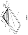
- filters are mounted to the upper dampproofing layer, disposed between the UV coating layer and the transparent electrode plate, to realize the display of a variety of colours.
- a method for making a luminous display comprising the steps of : disposing a lower electrode plate and a middle electrode plate on a lower dampproofing layer disposed on a rear surface member, an ionized layer being disposed between the electrode plates; spraying a mixture made of 67 % cyano ethyl celluloid solution and 33% luminous dust on the lower surface of a transparent electrode plate which is made from a mixture of 55 % IN 2 O 3 , 42% SnO 2 , and 3% hardening agent at the thickness of 1000 ⁇ ; heat-treating the transparent electrode plate at 500°C - 600°C to form a luminous phosphor layer between the transparent electrode plate and the middle delectrode plate; depositing a dampproofing layer, a UV coating layer, and a front surface member on the transparent electrode plate; and sealing the luminous display and all the layers using a frame placed around the edges of the luminous display.
- the middle and lower electrode plates are made by depositing a copper sulfide (CU 2 SO 4 ) solvent on an aluminium plate, drying the same, then heat treating the plates between 380°C - 430°C such that the lower and middle electrode plates have a high degree of electrical conductivity.
- CU 2 SO 4 copper sulfide
- the luminous dust includes 55% TiO 2 , 30% zinc oxide (ZnO) and 15% zinc sulfide (ZnSO 4 ) and the particles of said luminous dust are sized at 0.5-1 ⁇ m such that direct current is used in the luminous display.
- the luminous dust may be sized at 5-20 ⁇ m such that alternating current is used in the luminous display.
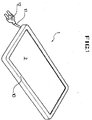
- reference numeral 1 denotes a luminous display according to a preferred embodiment of the present invention.
- a transparent electrode plate 7, middle, and lower electrode plates 8, and 88 and a luminous phosphor layer 9 are provided between a front surface member 2 and a rear surface member 3 of the luminous display.
- a dampproofing layer 5 is interposed between the rear surface member 3 and the lower electrode plate 88, and an ionized layer 6 is interposed between the lower electrode plate 88 and the middle electrode plate 8.
- the middle and lower electrode plates 8 and 88 are made by depositing a copper sulfide (CU 2 SO 4 ) solvent on an aluminium plate, then after drying, heat treating the plates between 380°C - 430°C such that the lower and middle electrode plates 8 and 88 have a high degree of electrical conductivity.
- CU 2 SO 4 copper sulfide
- a mixture made of 67% cyano ethyl celluloid solution and 33% luminous dust is sprayed on a lower surface of the transparent electrode plate 7, then the same undergoes a heat-treatment process at 500°C - 600°C. As a result, the luminous phosphor layer 9 is formed between the transparent electrode plate 7 and the middle electrode plate 8.
- the transparent electrode plate 7 is made from a mixture of 55% IN 2 O 3 , 42% SnO 2 , and 3% hardening agent which is sprayed then hardened at a thickness of 1000 ⁇ such that electrical resistance is minimized.
- a dampproofing layer 4 is provided on top of the transparent electrode plate 7, and a UV coating layer 2a is provided on top of the dampproofing layer 4.
- the front surface member 2 is placed on top of the UV coating layer 2a.
- a sealing frame 10 is placed around the luminous display 1 over the edges of the front and rear surface members 2 and 3 to seal all the layers therebetween. Electrical power is supplied to the luminous display 1 by an electrical wire 11 and a plug 12 which are connected to the electrode plate 7, 8 and 88. With the supply of electrical power, light is emitted from the luminous phosphor layer 9 which passes through the transparent electrode plate 7, the dampproofing layer 4, and the UV coating layer 2a to be radiated out the front surface member 2.
- the luminous display 1 structured as in the above it is preferable to add a compound to allow different levels of illumination to be controlled and colours to be varied. Such an addition allows both direct and alternating current to be used, and the control of the level of illumination from 40Lit to 800Lit.
- the luminous phosphor layer 9 is formed by spraying a compound comprised of 67 % cyano ethyl celluloid solution and 33 % luminous dust on the lower surface of the transparent electrode plate 7, then heat treating the compound at 500°C - 600°C.
- the above luminous dust includes 55% TiO 2 , 30% zinc oxide (ZnO), and 15 % zinc sulfide (ZnSO 4 ). If the size of the luminous dust particles is set at 0.5-1 ⁇ m and the particles amassed, direct current can be used in the luminous display 1. However, when the size of the dust particles is set at 5-20 ⁇ m and the particles separated, alternating can be used in the luminous display 1.
- a thickness of the luminous phosphor layer 9 is within a range of 5000-6000 ⁇ with a ⁇ 3% deviation.
- the transparent electrode plate 7 is formed on the luminous phosphor layer 9 from a mixture of 55% In 2 O 3 , 42% SnO 2 , and 3% hardening agent at a thickness of 1000 ⁇ . Accordingly, the resistance value of the transparent electrode plate 7 is minimized to 10 -5 ⁇ such that only a small amount of electricity is consumed.
- the middle and lower electrode plates 8 and 88 are made by depositing a copper sulfide (CU 2 SO 4 ) solvent on an aluminium plate, drying the solvent, and heat treating the plates between 380° - 430°C.
- CU 2 SO 4 copper sulfide
- the lower and middle electrode plates 8 and 88 have a high degree of electrical conductivity, allowing the overall size of the luminous display 1 to be substantially enlarged without the lower and middle electrode plates 8 and 88 warping, while preventing the generation of a potential difference and a reduction in illumination.
- the electricity usage is kept to a minimum by utilizing only 0.5W - 5W per 1 m 2 .
- the display allows both direct and alternating current of 6V - 220V to be used, the size of the display can be greatly increased and the shape altered in a variety of ways, and can realize an assortment of colours and levels of illumination enabling the display to be used for commercial purposes as well as in the home.
Landscapes
- Engineering & Computer Science (AREA)
- Manufacturing & Machinery (AREA)
- Illuminated Signs And Luminous Advertising (AREA)
- Luminescent Compositions (AREA)
- Investigating, Analyzing Materials By Fluorescence Or Luminescence (AREA)
- Vessels And Coating Films For Discharge Lamps (AREA)
Applications Claiming Priority (4)
| Application Number | Priority Date | Filing Date | Title |
|---|---|---|---|
| KR9630721 | 1996-07-26 | ||
| KR19960030721 | 1996-07-26 | ||
| KR1019970033990A KR100231297B1 (ko) | 1996-07-26 | 1997-07-21 | 장식용 발광체 및 그 제조방법 |
| KR9733990 | 1997-07-21 |
Publications (2)
| Publication Number | Publication Date |
|---|---|
| EP0821545A2 true EP0821545A2 (de) | 1998-01-28 |
| EP0821545A3 EP0821545A3 (de) | 1998-08-05 |
Family
ID=26632041
Family Applications (1)
| Application Number | Title | Priority Date | Filing Date |
|---|---|---|---|
| EP97305582A Withdrawn EP0821545A3 (de) | 1996-07-26 | 1997-07-25 | Leuchtanzeige und Verfahren zu ihrer Herstellung |
Country Status (6)
| Country | Link |
|---|---|
| EP (1) | EP0821545A3 (de) |
| JP (1) | JPH10133609A (de) |
| KR (1) | KR100231297B1 (de) |
| CA (1) | CA2211452C (de) |
| ID (1) | ID17542A (de) |
| TW (1) | TW350966B (de) |
Cited By (2)
| Publication number | Priority date | Publication date | Assignee | Title |
|---|---|---|---|---|
| EP1014329A3 (de) * | 1998-12-23 | 2001-05-09 | Helmut Dipl.-Ing. Habel | Selbstleuchtendes Informationssymbol mit Elektrolumineszfolien |
| EP1662573A3 (de) * | 2004-11-25 | 2006-08-16 | Samsung SDI Co., Ltd. | Flachbildschirm und Verfahren zu dessen Herstellung |
Families Citing this family (1)
| Publication number | Priority date | Publication date | Assignee | Title |
|---|---|---|---|---|
| KR100990668B1 (ko) * | 2008-04-03 | 2010-10-29 | (주)엘지하우시스 | 면조명 수단을 갖는 목재 도어 |
Family Cites Families (6)
| Publication number | Priority date | Publication date | Assignee | Title |
|---|---|---|---|---|
| JPS5842960B2 (ja) * | 1980-06-13 | 1983-09-22 | 双葉電子工業株式会社 | エレクトロルミネセンス装置 |
| JPH0290489A (ja) * | 1988-09-28 | 1990-03-29 | Hitachi Ltd | 分散型el素子 |
| JPH02239592A (ja) * | 1989-03-14 | 1990-09-21 | Seiko Epson Corp | 薄膜エレクトロルミネッセンス素子及びその駆動方法及び画像読み取り装置 |
| JPH04280094A (ja) * | 1991-03-07 | 1992-10-06 | Sony Corp | 薄膜発光素子 |
| JPH05290973A (ja) * | 1992-04-14 | 1993-11-05 | Sumitomo Chem Co Ltd | Elランプ |
| JPH07142173A (ja) * | 1993-11-22 | 1995-06-02 | Toshiba Electron Eng Corp | 有機分散型elパネル |
-
1997
- 1997-07-21 KR KR1019970033990A patent/KR100231297B1/ko not_active Expired - Fee Related
- 1997-07-25 EP EP97305582A patent/EP0821545A3/de not_active Withdrawn
- 1997-07-25 CA CA002211452A patent/CA2211452C/en not_active Expired - Fee Related
- 1997-07-26 TW TW086110648A patent/TW350966B/zh active
- 1997-07-28 ID IDP972619A patent/ID17542A/id unknown
- 1997-07-28 JP JP9201520A patent/JPH10133609A/ja active Pending
Cited By (3)
| Publication number | Priority date | Publication date | Assignee | Title |
|---|---|---|---|---|
| EP1014329A3 (de) * | 1998-12-23 | 2001-05-09 | Helmut Dipl.-Ing. Habel | Selbstleuchtendes Informationssymbol mit Elektrolumineszfolien |
| EP1662573A3 (de) * | 2004-11-25 | 2006-08-16 | Samsung SDI Co., Ltd. | Flachbildschirm und Verfahren zu dessen Herstellung |
| US7355344B2 (en) | 2004-11-25 | 2008-04-08 | Samsung Sdi Co., Ltd. | Flat panel display and method of manufacturing the same |
Also Published As
| Publication number | Publication date |
|---|---|
| KR100231297B1 (ko) | 1999-11-15 |
| KR980013532A (ko) | 1998-04-30 |
| CA2211452A1 (en) | 1998-01-26 |
| TW350966B (en) | 1999-01-21 |
| ID17542A (id) | 1998-01-08 |
| JPH10133609A (ja) | 1998-05-22 |
| EP0821545A3 (de) | 1998-08-05 |
| CA2211452C (en) | 2001-10-30 |
Similar Documents
| Publication | Publication Date | Title |
|---|---|---|
| EP2008291B1 (de) | Elektrisches installationsgerät | |
| CA1105429A (en) | Multi-panel electroluminescent light assembly | |
| US6965196B2 (en) | Electroluminescent sign | |
| TWI524566B (zh) | 發光裝置、照明裝置、光學顯示裝置、緊急照明裝置、汽車用室內照明裝置、傢俱、建築材料、玻璃化物、顯示器、收納傢俱 | |
| US5586879A (en) | Fluorescent electroluminescent lamp | |
| EP0794689B1 (de) | Lumineszenzelement mit einer lichtdurchlässigen Reflexionsschicht und Verfahren zur Herstellung desselben | |
| US20100188246A1 (en) | Inorganic thick film ac electroluminescence element having at least two inputs, and production method and use | |
| CA2299684A1 (en) | Electroluminescent sign | |
| US6284983B1 (en) | Multifunctional printed circuit board with an opto-electronically active component | |
| AU2006271435B2 (en) | Electroluminescent one-way vision panel | |
| JPH08203669A (ja) | El両面発光表示体 | |
| TW200428313A (en) | Full color display panel with mirror function | |
| CA2211452C (en) | Luminous display and a manufacturing method thereof | |
| US6639355B1 (en) | Multidirectional electroluminescent lamp structures | |
| CA2475961A1 (en) | Electroluminescence device | |
| US20080218075A1 (en) | Electroluminescent Displays | |
| TW350962B (en) | A double-layer phosphor screen and a process for preparing the same | |
| JP2947154B2 (ja) | 電界発光素子 | |
| CN112920732B (zh) | 一种电致发光量子变色膜 | |
| CN2251770Y (zh) | 电子荧光指示牌 | |
| US20030030383A1 (en) | Process for the manufacture of an electroluminescent film and application of such a film | |
| KR20090034248A (ko) | 문양을 가지는 가전제품용 발광패널의 제조방법과 이를이용한 발광패널 | |
| CN2262757Y (zh) | 平面板式霓虹灯 | |
| JPH0831572A (ja) | 電界発光表示素子 | |
| CN115634816A (zh) | 一种电致荧光发光漆涂层工艺 |
Legal Events
| Date | Code | Title | Description |
|---|---|---|---|
| PUAI | Public reference made under article 153(3) epc to a published international application that has entered the european phase |
Free format text: ORIGINAL CODE: 0009012 |
|
| 17P | Request for examination filed |
Effective date: 19970812 |
|
| AK | Designated contracting states |
Kind code of ref document: A2 Designated state(s): DE FR GB IT |
|
| PUAL | Search report despatched |
Free format text: ORIGINAL CODE: 0009013 |
|
| AK | Designated contracting states |
Kind code of ref document: A3 Designated state(s): AT BE CH DE DK ES FI FR GB GR IE IT LI LU MC NL PT SE |
|
| AKX | Designation fees paid |
Free format text: DE FR GB IT |
|
| RBV | Designated contracting states (corrected) |
Designated state(s): DE FR GB IT |
|
| 17Q | First examination report despatched |
Effective date: 20010703 |
|
| STAA | Information on the status of an ep patent application or granted ep patent |
Free format text: STATUS: THE APPLICATION IS DEEMED TO BE WITHDRAWN |
|
| 18D | Application deemed to be withdrawn |
Effective date: 20011114 |