EP0822452A2 - Méthode et dispositif de correction de l'effet de proximité optique - Google Patents
Méthode et dispositif de correction de l'effet de proximité optique Download PDFInfo
- Publication number
- EP0822452A2 EP0822452A2 EP97103090A EP97103090A EP0822452A2 EP 0822452 A2 EP0822452 A2 EP 0822452A2 EP 97103090 A EP97103090 A EP 97103090A EP 97103090 A EP97103090 A EP 97103090A EP 0822452 A2 EP0822452 A2 EP 0822452A2
- Authority
- EP
- European Patent Office
- Prior art keywords
- optical proximity
- proximity correction
- feature
- value
- edge
- Prior art date
- Legal status (The legal status is an assumption and is not a legal conclusion. Google has not performed a legal analysis and makes no representation as to the accuracy of the status listed.)
- Withdrawn
Links
- 238000012937 correction Methods 0.000 title claims abstract description 144
- 230000003287 optical effect Effects 0.000 title claims abstract description 96
- 238000000034 method Methods 0.000 title claims abstract description 65
- 230000009021 linear effect Effects 0.000 claims abstract description 88
- 238000013461 design Methods 0.000 claims abstract description 76
- 230000014509 gene expression Effects 0.000 claims abstract description 55
- 238000000206 photolithography Methods 0.000 claims abstract description 14
- 238000003909 pattern recognition Methods 0.000 claims abstract description 6
- 230000000903 blocking effect Effects 0.000 claims description 7
- 238000005286 illumination Methods 0.000 description 22
- 230000005855 radiation Effects 0.000 description 18
- 230000008569 process Effects 0.000 description 16
- 238000012360 testing method Methods 0.000 description 14
- VYZAMTAEIAYCRO-UHFFFAOYSA-N Chromium Chemical compound [Cr] VYZAMTAEIAYCRO-UHFFFAOYSA-N 0.000 description 9
- 238000013213 extrapolation Methods 0.000 description 9
- 229910052804 chromium Inorganic materials 0.000 description 8
- 239000011651 chromium Substances 0.000 description 8
- 238000002474 experimental method Methods 0.000 description 8
- 239000011521 glass Substances 0.000 description 8
- 239000000758 substrate Substances 0.000 description 8
- 230000000694 effects Effects 0.000 description 7
- XUIMIQQOPSSXEZ-UHFFFAOYSA-N Silicon Chemical compound [Si] XUIMIQQOPSSXEZ-UHFFFAOYSA-N 0.000 description 6
- 229910052710 silicon Inorganic materials 0.000 description 6
- 239000010703 silicon Substances 0.000 description 6
- 238000012886 linear function Methods 0.000 description 5
- 230000003247 decreasing effect Effects 0.000 description 4
- 238000004519 manufacturing process Methods 0.000 description 4
- 229920002120 photoresistant polymer Polymers 0.000 description 4
- 239000000463 material Substances 0.000 description 3
- 238000007620 mathematical function Methods 0.000 description 3
- 238000001465 metallisation Methods 0.000 description 3
- 230000007704 transition Effects 0.000 description 3
- 230000008901 benefit Effects 0.000 description 2
- 238000004364 calculation method Methods 0.000 description 2
- 230000008859 change Effects 0.000 description 2
- 238000011161 development Methods 0.000 description 2
- 238000010586 diagram Methods 0.000 description 2
- 238000005516 engineering process Methods 0.000 description 2
- 229910021420 polycrystalline silicon Inorganic materials 0.000 description 2
- 229920005591 polysilicon Polymers 0.000 description 2
- 238000000926 separation method Methods 0.000 description 2
- 238000012217 deletion Methods 0.000 description 1
- 230000037430 deletion Effects 0.000 description 1
- 239000003989 dielectric material Substances 0.000 description 1
- 238000004836 empirical method Methods 0.000 description 1
- 238000007667 floating Methods 0.000 description 1
- 230000004927 fusion Effects 0.000 description 1
- 239000007943 implant Substances 0.000 description 1
- 230000009022 nonlinear effect Effects 0.000 description 1
- 238000004886 process control Methods 0.000 description 1
- 239000000047 product Substances 0.000 description 1
- 238000004626 scanning electron microscopy Methods 0.000 description 1
- 238000005549 size reduction Methods 0.000 description 1
- 238000004513 sizing Methods 0.000 description 1
- 238000001228 spectrum Methods 0.000 description 1
- 239000013589 supplement Substances 0.000 description 1
- 210000003462 vein Anatomy 0.000 description 1
Images




Classifications
-
- G—PHYSICS
- G03—PHOTOGRAPHY; CINEMATOGRAPHY; ANALOGOUS TECHNIQUES USING WAVES OTHER THAN OPTICAL WAVES; ELECTROGRAPHY; HOLOGRAPHY
- G03F—PHOTOMECHANICAL PRODUCTION OF TEXTURED OR PATTERNED SURFACES, e.g. FOR PRINTING, FOR PROCESSING OF SEMICONDUCTOR DEVICES; MATERIALS THEREFOR; ORIGINALS THEREFOR; APPARATUS SPECIALLY ADAPTED THEREFOR
- G03F7/00—Photomechanical, e.g. photolithographic, production of textured or patterned surfaces, e.g. printing surfaces; Materials therefor, e.g. comprising photoresists; Apparatus specially adapted therefor
- G03F7/70—Microphotolithographic exposure; Apparatus therefor
- G03F7/70425—Imaging strategies, e.g. for increasing throughput or resolution, printing product fields larger than the image field or compensating lithography- or non-lithography errors, e.g. proximity correction, mix-and-match, stitching or double patterning
- G03F7/70433—Layout for increasing efficiency or for compensating imaging errors, e.g. layout of exposure fields for reducing focus errors; Use of mask features for increasing efficiency or for compensating imaging errors
- G03F7/70441—Optical proximity correction [OPC]
-
- G—PHYSICS
- G03—PHOTOGRAPHY; CINEMATOGRAPHY; ANALOGOUS TECHNIQUES USING WAVES OTHER THAN OPTICAL WAVES; ELECTROGRAPHY; HOLOGRAPHY
- G03F—PHOTOMECHANICAL PRODUCTION OF TEXTURED OR PATTERNED SURFACES, e.g. FOR PRINTING, FOR PROCESSING OF SEMICONDUCTOR DEVICES; MATERIALS THEREFOR; ORIGINALS THEREFOR; APPARATUS SPECIALLY ADAPTED THEREFOR
- G03F1/00—Originals for photomechanical production of textured or patterned surfaces, e.g., masks, photo-masks, reticles; Mask blanks or pellicles therefor; Containers specially adapted therefor; Preparation thereof
- G03F1/36—Masks having proximity correction features; Preparation thereof, e.g. optical proximity correction [OPC] design processes
Definitions
- the present invention relates to photolithography techniques. More particularly, the invention relates to improved methods and apparatuses for performing optical proximity correction.
- Photolithography involves selectively exposing regions of a resist coated silicon wafer to a radiation pattern, and then developing the exposed resist in order to selectively protect regions of wafer layers (e.g., regions of substrate, polysilicon, or dielectric).
- regions of wafer layers e.g., regions of substrate, polysilicon, or dielectric.
- An integral component of photolithographic apparatus is a reticle which includes a pattern corresponding to features at one layer in an IC design.
- Such reticle typically includes a transparent glass plate covered with a patterned light blocking material such as chromium.
- the reticle is placed between a radiation source producing radiation of a pre-selected wavelength and a focusing lens which may form part of a stepper apparatus. Placed beneath the stepper is a resist covered silicon wafer.
- the radiation from the radiation source is directed onto the reticle, light passes through the glass (regions not having chromium patterns) and projects onto the resist covered silicon wafer. In this manner, an image of the reticle is transferred to the resist.
- the resist (sometimes referred to as a photoresist ) is provided as a thin layer of radiation-sensitive material that is spin-coated over the entire silicon wafer surface.
- the resist material is classified as either positive or negative depending on how it responds to light radiation.
- Positive resist when exposed to radiation becomes more soluble and is thus more easily removed in a development process.
- a developed positive resist contains a resist pattern corresponding to the dark regions on the reticle.
- Negative resist in contrast, becomes less soluble when exposed to radiation. Consequently, a developed negative resist contains a pattern corresponding to the transparent regions of the reticle.
- the following discussion will describe only positive resists, but it should be understood that negative resists may be substituted therefor.
- Figure 1A shows a hypothetical reticle 100 corresponding to an IC layout pattern.
- the IC pattern consists of three rectangular design features.
- a clear reticle glass 110 allows radiation to project onto a resist covered silicon wafer.
- Three rectangular chromium regions 102, 104 and 106 on reticle glass 110 block radiation to generate an image corresponding to intended IC design features.
- Figure 1B illustrates how diffraction and scattering affect an illumination pattern produced by radiation passing through reticle 100 and onto a section of silicon substrate 120.
- the illumination pattern contains an illuminated region 128 and three dark regions 122, 124, and 126 corresponding to chromium regions 102, 104, and 106 on reticle 100.
- the illuminated pattern exhibits considerable distortion, with dark regions 122, 124, and 126 having their corners rounded and their feature widths reduced.
- Other distortions commonly encountered in photolithography include fusion of dense features and shifting of line segment positions.
- any distorted illumination pattern propagates to a developed resist pattern and ultimately to IC features such as polysilicon gate regions, vias in dielectrics, etc. As a result, the IC performance is degraded or the IC becomes unusable.
- OPC optical proximity correction
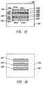
- Figure 1C illustrates how optical proximity correction may be employed to modify the reticle design shown in Figure 1A and thereby better provide the desired illumination pattern.
- a corrected reticle 140 includes three base rectangular features 142, 144, and 146 outlined in chromium on a glass plate 150.
- Various corrections have been added to these base features.
- Some correction takes the form of serifs 148a-148f and 149a-149f.
- Serifs are small appendage-type addition or subtraction regions typically made at corner regions on reticle designs.
- the serifs are square chromium extensions protruding beyond the comers of base rectangles 142, 144, and 146. These features have the intended effect of sharpening the corners of the illumination pattern on the wafer surface.
- the reticle 140 includes segments 151a-151d to compensate for feature thinning known to result from optical distortion.
- Figure 1D shows an illumination pattern 160 produced on a wafer surface 160 by radiation passing through the reticle 140.
- the illuminated region includes a light region 168 surrounding a set of dark regions 162, 164 and 166 which rather faithfully represent the intended pattern shown in Figure 1A.
- the degree of optical proximity correction i.e., the size and location of correction segments
- the degree of optical proximity correction depends upon the desired IC feature size and the location of such feature with respect to other IC features.
- the width of any one of segments 151a-151d may have to be increased or decreased if the width of any of the base rectangles 142, 144, and 146 is increased or decreased or if the spacing between any of these base rectangles is increased or decreased.
- the degree of correction necessary for a given feature is determined largely by empirical methods. That is, experiments are conducted with reticles having test patterns to determine the illumination pattern produced on a wafer by light shown through the test pattern. The deviation between the actual illumination pattern and the desired feature pattern is used to determine how much optical proximity correction is required for a reticle used to produce the desired feature pattern.
- the reticle 100 of Figure 1A may be used as a test reticle. A single experiment would show that the illumination pattern produced by reticle 100 corresponds to that shown in Figure 1B. The rounding and thinning effects observed would lead an OPC designer to specify that when the pattern of Figure 1A is desired, the corrections shown in Figure 1C should be employed. Specifically, the designer would specify the width and location of segments 151a-151d and serifs 148a-148f and 149a-149f.
- the degree of optical proximity correction can be estimated with good accuracy by interpolating linearly between the actual amount of correction found to be necessary for two test patterns straddling (in terms of sizing and/or spacing) a real feature on an IC design. Further, the degree of correction for very small patterns lying beyond a range of experimental patterns may often be predicted with good accuracy by linear extrapolation. Because these techniques require that only a relatively few test reticles be generated, many OPC systems in use today employ such linear interpolation and extrapolation techniques.
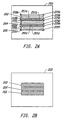
- Figure 2A shows a reticle 200 having critical dimensions below a linear threshold (e.g., below about 0.5 microns).
- a linear optical proximity correction is performed to correct for optical distortions expected in the linear regime, the resulting illumination pattern is unacceptably distorted.
- serifs 228a-228f and 229a-229f and segments 251a-251d can be added to the reticle design in a manner predicted by conventional linear interpolation/extrapolation, inappropriate fusing and thinning of bars 262, 264, and 266 appear in the illumination pattern on a substrate 260 as shown in Figure 2B.
- the present invention fills this need by providing an optical proximity correction method which employs a non-linear mathematical function for determining the amount of correction required for an arbitrary IC pattern having dimensions in the non-linear correction regime.
- the non-linear function should be developed to accurately depict the variation in required optical proximity correction with decreasing critical dimension in the non-linear regime described above.
- the present invention provides an optical proximity correction method which can be characterized as including the following steps: (a) performing pattern recognition on an integrated circuit layout design to identity a location of a selected feature edge in the layout design; (b) obtaining an optical proximity correction value for the selected feature edge by evaluating one or more non-linear mathematical expressions for optical proximity correction at the location of the selected feature edge; and (c) incorporating the optical proximity correction value into the layout design to form a reticle design.
- the above steps are repeated many times to scan multiple feature edges in the layout design.
- the method preferably determines whether that feature edge is associated with a feature having a critical dimension above a pre-selected value. If so, the method skips steps (b) and (c) above. In this manner, unnecessary computation is avoided as larger features reap relatively little benefit from OPC.
- the pre-selected value is about 0.5 ⁇ m or greater: at least for conventional photolithography performed with ultra-violet radiation.
- the non-linear mathematical expression(s) may be evaluated by directly solving the expression. However, for computation efficiency, it may be desirable to store the expression as a series of discreet optical proximity correction values generated from the non-linear mathematical expression. Then when a feature edge is to be evaluated, the degree of correction is picked off of a look-up table of discreet points rather than solving a complicated mathematical expression.
- the non-linear mathematical expressions are evaluated at coordinates provided as combinations of at least (i) one value representing the width of a light transmitting region adjacent to the selected feature edge, and (ii) a second value representing a width of a light blocking region adjacent to the selected feature edge.
- the degree of correction is a function of both the feature width and the interfeature spacing adjacent the feature.
- the resulting correction is sometimes confirmed against one or more predetermined rules.
- Such rules may specify the minimum spacing between adjacent light blocking regions for a particular design family.
- the invention provides an apparatus for performing optical proximity correction on layout designs to be used in photolithography.
- the apparatus may be characterized as including the following components: (a) means for performing pattern recognition on an integrated circuit layout design to identify locations of selected feature edges in the layout design; and (b) means for obtaining an optical proximity correction value for at least one of the selected feature edges by evaluating one or more non-linear mathematical expressions for optical proximity correction at the location of the at least one selected feature edge.
- the apparatus includes means for determining whether the selected feature edges are associated with features having a critical dimension of at most about a predefined value. When such means for determining finds that a particular feature edge is associated with a feature having a critical dimension greater than the predefined value, an optical proximity correction value is not obtained.
- the apparatus of this invention will preferably be implemented as software on a digital computer system. This is particularly convenient, as most IC designs are today provided in digital form.
- the software of this invention simply acts on the IC designs as described to generate a reticle design which can be printed on an actual reticle.
- Figure 1A illustrates a conventional reticle having an IC design pattern outlined in, for example, chromium on a glass backing.
- Figure 1B shows an illumination pattern produced on a substrate by light shown through the reticle of Figure 1A.
- the illumination pattern exhibits rounding and thinning effects that result when no optical proximity correction is performed.
- Figure 1C illustrates a conventional reticle design employing optical proximity correction to overcome the rounding and thinning effects in the illumination pattern of Figure 1B.
- Figure 1D shows an improved illumination pattern produced on a substrate by light shown through the optical proximity corrected reticle of Figure 1C.
- Figure 2A illustrates a conventional optical proximity corrected reticle design for an IC design having critical dimensions in a non-linear correction regime.
- Figure 2B shows a resulting fused illumination image produced on a substrate by light shown through the reticle of Figure 2A.
- Figure 3 shows, in accordance with one aspect of the present invention, a plurality of experimentally determined OPC values plotted as functions feature size and spacing size (critical dimensions) for patterns in the linear and non-linear regimes.
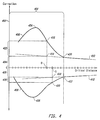
- Figure 4 illustrates, in one embodiment, a mathematical expression designed to express OPC values as functions feature size and spacing size (critical dimensions) for patterns in the linear and non-linear regimes.
- Figure 5 illustrates, an exemplary reticle test pattern used to generate a empirical OPC corrections necessary to derive the mathematical function presented in Figure 4.
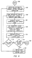
- Figure 6 is a process flow diagram illustrating the steps involved in developing a corrected reticle design in accordance with one embodiment of this invention.
- Figure 7A illustrates a novel reticle design employing optical proximity correction obtained from a non-linear function to overcome the problematic effects noted in the illumination pattern of Figure 2B.
- Figure 7B shows an improved illumination pattern produced on a substrate by light shown through the optical proximity corrected reticle of Figure 7A.
- Figures 1A-D and 2A-B illustrate that some conventional optical proximity correction methods are unable to correct reticle design patterns having very small critical dimensions (e.g., below about 0.5 microns).
- the present invention utilizes non-linear mathematical expressions to ascertain the degree of correction required for any such patterns having critical dimensions in such non-linear domain.
- the necessary non-linear mathematical expressions may be generated by various means. In a preferred embodiment, they are generated by curve fitting data from experiments on incrementally sized reticle designs having critical dimensions in the non-linear region. They may also be generated from computer simulated data of patterns having critical dimensions in the non-linear region.
- FIG. 3 there is shown a graph 300 including mock experimental optical proximity correction values plotted versus (1) a critical dimensions based upon feature size (plotted above the horizontal axis), and (2) critical dimensions based upon spacing between features (plotted below the horizontal axis).
- a critical dimension based upon feature size might be the width of dark region 122 shown in Figure 1B
- a critical dimension based upon spacing might be the distance between dark regions 122 and 124 in Figure 1B.
- the features described herein correspond to IC features such as transistor gate electrodes, metallization conductive lines and the like.
- representative data points taken from hypothetical test reticles are plotted on a grid having a vertical axis 328 representing optical proximity correction values and a horizontal axis 326 representing the critical dimension (in feature size and spacing between features).
- optical proximity correction values vary in a generally linear manner.
- the optical proximity correction values vary non-linearly.
- points 302, 304, 306, 308, 310, and 312 specify the degree of correction for feature widths in the non-linear regime
- points 280, 282, and 284 specify the degree of correction for feature widths in the linear regime.
- points 314, 316, 318, 320, 322, and 324 specify the degree of correction required for interfeature spacing in the non-linear regime
- points 334, 336, and 338 specify the degree of correction required for interfeature spacing in the linear regime.
- the transition between linear and non-linear domains sometimes corresponds to a critical dimension of approximately 0.5 microns for both feature width and interfeature spacing.
- the transition between the linear and non-linear regions may occur more gradually than depicted in Figure 3.
- Figure 4 presents a graphical representation 400 of two non-linear mathematical expressions 406 and 408 which provide optical proximity correction values as a continuous function of feature width (in the case of expression 406) and interfeature spacing (in the case of expression 408).
- a vertical axis 402 specifies the value of optical proximity correction
- a horizontal axis specifies critical dimension.
- expression 406 is generated by curve fitting feature width test data
- curve 408 is generated by curve fitting interfeature spacing test data (such as the data illustrated in Figure 3).
- the resulting mathematical expressions have an identifiable non-linear region 401 which extends below point 430 for expression 406, and below point 432 for expression 408. Above points 430 and 432, the expressions 406 and 408 vary in a substantially linear fashion.
- the non-linear expressions generated in accordance with this invention are devised to apply a relatively wide range expected photolithography conditions.
- a single expression or group of expressions
- such expression(s) could be used with various photolithography systems which may employ different light intensities for example.
- the figure illustrates the difficulty associated with applying a conventional linear interpolation/extrapolation technique to reticle designs for features having critical dimensions in the non-linear domain. For example, if a hypothetical feature edge has an associated width B, then the correct optical proximity correction value for that feature edge would be identified with a point 416 on non-linear curve 406. Unfortunately if instead of the non-linear correction employed with the present invention, a conventional linear extrapolation technique was employed, a correction value associated with a point 414 would be obtained. As can be seen, point 414 is located on a line 410 extrapolated from known correction values associated with larger critical dimensions in the linear regime, and the linear correction value associated with point 414 is separated from the non-linear correction value associated with point 416 by an increment 422.
- the amount of optical proximity correction varies non-linearly for critical dimensions below a threshold region (e.g., about 0.5 microns).
- the present invention builds on this recognition by generating non-linear mathematical expressions which accurately represent optical proximity correction values for reticle designs having feature widths and/or feature spacings in the non-linear regime.
- curves 406 and 408 change direction at points 434 and 436, respectively. While the present invention can in theory be applied to features having critical dimensions smaller than points 434 and 436, such features are typically too small to be imaged with radiation at conventional wavelengths (e.g., the visible or ultra-violet regions of the electromagnetic spectrum). As a result, shorter wavelength radiation (e.g., X-rays) must be used to image smaller feature patterns.
- conventional wavelengths e.g., the visible or ultra-violet regions of the electromagnetic spectrum.
- shorter wavelength radiation e.g., X-rays
- the non-linear mathematical expressions of this invention may be analytic expressions (e.g., polynomials) or numerical expressions.
- V OPC f(x,y,z)
- V OPC is the value of the optical proximity correction
- f(x,y,z) is an analytic or numerical expression of the variables x, y, and z.
- only a single variable is used in the expression. That variable might be the value of the feature width or the interfeature spacing at a location of interest.
- two or even three variables may be employed in the same expression. These may be the feature width, the interfeature spacing, the angle of a feature, or any of a number of other parameters associated with the feature edge of interest
- the non-linear mathematical expression is stored as a comprehensive lookup table constructed by evaluating the expression at numerous critical dimension values. Using such lookup tables generally simplifies software operations and speeds up computation.
- Figure 5 shows a simple standardized reticle test pattern 500 known as a paddle structure which may be used to generate data for use in preparing a non-linear expression in accordance with this invention.
- a resist coated wafer is exposed to light passing through reticle 500.
- the resist is subsequently developed and the resulting pattern is evaluated with scanning electron microscopy to determine the degree of necessary correction.
- the paddle structure has been found to efficiently provide various types of data. Specifically, the structure includes both a dense collection of features in its lower portion (bars 502, 504, 506, 508, and 509) and an isolated feature in its upper portion (bar 506).
- the amount of correction required is a function of the local feature density, with isolated features requiring a certain amount and type of correction and dense features sometimes requiring a different amount and type of correction.
- Figure 6 illustrates a process of the present invention for performing optical proximity correction in the non-linear regime.
- the process begins at 700 and in a step 702 determines which integrated circuit design level will be subjected to optical proximity correction.
- integrated circuits are formed with many different mask levels, each of which requires its own reticle. For example, one level may define the pattern for a p-type well implant, another level may define a transistor gate electrode pattern, yet another level may define a first metallization interconnection pattern, etc.
- a design layout for a single level is selected for correction at step 702.
- the initial layout design for the selected layout level is obtained and a scan of its features is started at a step 704.
- the scanning process begins at an arbitrarily selected position of the layout design and proceeds in a defined direction until a feature edge is located. Such edge represents the boundary of a protected and unprotected region on a mask.
- the method proceeds to a step 706 where coordinates associated with the current edge are generated. In a preferred embodiment, these coordinates include (1) the width of the feature (e.g., the protected region) at the current edge, and (2) the width of the space (e.g., the unprotected region) between the current edge and the edge of the next adjacent feature.
- the second coordinate has been referred to above as the interfeature spacing.
- the method includes an additional step of determining whether a feature size exceeds a critical dimension (e.g., one micron). If so, current edge is ignored and the next edge is located. This may substantially improve the computational efficiency of the method by eliminating unnecessary correction calculations.
- a critical dimension e.g., one micron
- step 708 the coordinates are evaluated with a non-linear mathematical expression obtained as described above in connection with Figure 4.
- a particular value of optical proximity correction may be obtained for a feature width or an interfeature spacing or both. If both the feature width and the interfeature spacing are used to determine the correction, the non-linear correction expression should be written as a function of at least those two variables. In such cases, the two curves 406 and 408 shown in Figure 4 would have to be merged in a single function that could be depicted in three-dimensional space.
- a step 710 performs a correction on the current edge. For example, the feature width may be increased or reduced at that edge, a serif may be added at the edge (see Figure 1C for example), etc. In addition, correction may also entail shifting entire features in an attempt to prevent features from fusing together.
- the method proceeds to a step 712 where a decision is made as to whether anymore edges are present in the current IC design layout level. If there are more edges, then process control reverts to step 702 where the next edge is identified by scanning in the original direction until the next edge is located. At that point, the new edge becomes the current edge and process steps 706, 708, and 710 are performed at the new current edge. Then, it is determined at step 712 whether any more edges are present.
- step 714 it is determined whether there are any more design levels. If there are more design levels, the method proceeds to a step 716 where the next design level is obtained. For example, if a layout for a via level has just been completely corrected, step 716 may obtain the design layout for a first metallization layer to be formed immediately on top of the via level. From step 716, the method proceeds to step 702, and from there through steps 704, 706, 708, 710, 712, and if no more edges are present for that level, then the method proceeds to step 714. When all design layout levels to be corrected have been corrected (i.e., decision step 714 is answered in the negative), then the optical proximity correction method is completed at 718.
- the above method is typically implemented as software on a digital computer system.
- the IC layout designs are provided as digitized patterns defining a desired mask layout on a chip. These digitized patterns are scanned with pattern recognition software which can identify edges and associated feature/spacing sizes. The pattern recognition software may even identify and choose to ignore features that are greater than a predefined size, e.g., one micron.
- the completely corrected reticle design is formed on an actual reticle such as a glass and chrome reticle.
- the non-linear optical proximity correction function may be provided in the form of a programmed equation that can be directly evaluated for each set of coordinates that it receives. More preferably, however, the non-linear function is initially evaluated at numerous dimensions and stored in the form of a look-up table containing a series of discreet points corresponding to correction values for the corresponding feature dimensions. When a new coordinate is provided by the pattern recognition software, the nearest point from the look-up table is identified and used to provide the necessary correction value. Storing the non-linear mathematical function in the form of a look-up table significantly improves computational efficiency.
- paddle pattern of Figure 5 will now be assumed to be an IC design pattern that is to be subjected to non-linear optical proximity correction.
- paddle structure 500 has four identically sized features (bars) 502, 504, 508 and 509 straddling a longer feature 506 having an isolated section at the top of the paddle pattern.
- the optical proximity correction software scans the paddle in a raster-like manner in order to identify all feature edges. During the scanning process, various edges are identified on paddle structure 500.
- the scanning process begins in the lower left corner of the pattern and proceeds horizontally across the pattern.
- the first feature edge encountered will be 530a.
- edge 530a becomes the current edge (step 704).
- appropriate coordinates are obtained, the degree of correction is ascertained, and the correction is made as described with respect to steps 706, 708, and 710.
- the pattern is horizontally scanned until the next feature edge 536a is identified. This edge is then evaluated per steps 706, 708, and 710.
- edges 536b, 536c,...536n are encountered, evaluated, and corrected as specified by the non-linear functions described above.
- the scanning process increments to a vertically adjacent position and again begins horizontal scanning. For example, the process may next encounter edge 530b. After evaluating and correcting that edge, the next successive edges are located and corrected as described until the right edge of the pattern is again encountered. At that point, the edge 530c is located and corrected. The scanning and correcting process continues in this manner through edge 528n where the pattern changes. At the next vertical increment, only a single feature will be found. Thus, after the top of bars 502, 504, 508, and 509 have been surpassed, the next edge encountered will be 522a. This edge is, of course, corrected as described above. The process thereafter continues through edges 522b, 520a, and 520b.
- the scanning process will then be repeated in a vertical rasterized manner to pick off and correct horizontally aligned edges.
- the diagonal scans may be employed in designs having lines and other features oriented diagonally with respect to the main grid of the chip.
- the feature width (e.g., the width of bar 502) forms one coordinate
- the interfeature spacing 510a between bar 502 and next adjacent bar 504 forms a second coordinate.
- Similar coordinates for edge 536b include the width of bar 504 and the spacing 510a
- the coordinates include the width of bar 504 and spacing 510b. Spacings 510c and 510d would be used in the coordinates of other edges.
- Edges with no close adjacent features will have a coordinate selected to indicate this condition (e.g. infinity).
- this condition e.g. infinity
- any feature separated from an adjacent feature by one micron or more will meet this condition. Certain rules may apply to correcting features with such edges.
- the scanning process preferably is programmed to ignore critical dimensions greater than about one micron. This is done to increase correction speed for critical dimensions in the non-linear regime. As mentioned above, slight distortions impact sub-micron IC features more severely than IC features having critical dimensions larger than about one micron. In addition, the greater the number of corrections performed, the greater the number of possible errors produced. For example, slivers may be inadvertently introduced in an attempt to correct a particular feature geometry. Silvers are common in optical proximity correction, and they many consist of small serifs or segments that are intended to append to an IC feature, but are inadvertently left floating (i.e., unattached to a feature). Thus, limiting optical proximity correction to sub-micron features increases efficiency and avoids introducing additional opportunities for errors.
- the method of the present invention may employ various design rules to supplement the correction values. Some of these rules may negate a correction provided by the non-linear expressions of this invention. Other rules may modify the correction value without negating the correction. Such rules are typically applied when a given feature and its local environment meet certain criteria Such rules may, for example, specify a minimum interfeature spacing for a particular design family. More specifically, such minimum interfeature may be selected to be between about 0.2 and 0.5 microns (which might be varied within this range by 0.01 microns).
- Figure 7A represents a reticle pattern having feature edges with critical dimensions in the non-linear regime (e.g., critical dimensions below about 0.5 microns).
- critical dimensions in the non-linear regime e.g., critical dimensions below about 0.5 microns.
- conventional optical proximity correction of an amount calculated for a linear case fails to prevent fusing in the developed resist regions.
- the non-linear optical proximity correction method of this invention is able to provide a correct degree of correction for very small features.
- a reticle 600 includes three symmetric features 602, 604, and 606.
- specific corrective segments and/or serifs were added.
- the particular corrective serifs include regions 628a through 628f and 629a through 629f appended to each of the corners of features 602, 604 and 606.
- segments 651a through 651d were added to prevent feature thinning.
- Figure 7B shows an illumination pattern produced on a substrate 660 by light shining through reticle 600.
- illumination pattern 660 includes three dark regions 662, 664, and 666 separated from one another.
- dark regions 662 and 664 are separated from one another by a light region 668.
- the illumination pattern created by a linearly corrected reticle e.g., see Figure 2B
- the fused resist structure of Figure 2B is a product of applying conventional optical proximity correction which fails to consider the non-linear behavior of correction associated with critical dimensions below a transition dimension (e.g., about 0.5 microns).
Landscapes
- Physics & Mathematics (AREA)
- General Physics & Mathematics (AREA)
- Preparing Plates And Mask In Photomechanical Process (AREA)
- Exposure And Positioning Against Photoresist Photosensitive Materials (AREA)
Applications Claiming Priority (2)
| Application Number | Priority Date | Filing Date | Title |
|---|---|---|---|
| US08/607,365 US5723233A (en) | 1996-02-27 | 1996-02-27 | Optical proximity correction method and apparatus |
| US607365 | 1996-02-27 |
Publications (2)
| Publication Number | Publication Date |
|---|---|
| EP0822452A2 true EP0822452A2 (fr) | 1998-02-04 |
| EP0822452A3 EP0822452A3 (fr) | 1998-05-13 |
Family
ID=24431963
Family Applications (1)
| Application Number | Title | Priority Date | Filing Date |
|---|---|---|---|
| EP97103090A Withdrawn EP0822452A3 (fr) | 1996-02-27 | 1997-02-26 | Méthode et dispositif de correction de l'effet de proximité optique |
Country Status (3)
| Country | Link |
|---|---|
| US (1) | US5723233A (fr) |
| EP (1) | EP0822452A3 (fr) |
| JP (2) | JP3151417B2 (fr) |
Cited By (6)
| Publication number | Priority date | Publication date | Assignee | Title |
|---|---|---|---|---|
| EP0928012A3 (fr) * | 1997-12-12 | 1999-07-14 | Lsi Logic Corporation | Méthode et dispositif de correction de l'effet de proximité optique |
| US6081659A (en) * | 1997-05-08 | 2000-06-27 | Lsi Logic Corporation | Comparing aerial image to actual photoresist pattern for masking process characterization |
| EP1094366A1 (fr) * | 1999-10-21 | 2001-04-25 | Infineon Technologies North America Corp. | Méthode pour corriger des effets de proximité optique |
| US6282696B1 (en) | 1997-08-15 | 2001-08-28 | Lsi Logic Corporation | Performing optical proximity correction with the aid of design rule checkers |
| US6426131B1 (en) | 1998-08-24 | 2002-07-30 | Lsi Logic Corporation | Off-axis pupil aperture and method for making the same |
| US6499003B2 (en) | 1998-03-03 | 2002-12-24 | Lsi Logic Corporation | Method and apparatus for application of proximity correction with unitary segmentation |
Families Citing this family (156)
| Publication number | Priority date | Publication date | Assignee | Title |
|---|---|---|---|---|
| JP3934719B2 (ja) * | 1995-12-22 | 2007-06-20 | 株式会社東芝 | 光近接効果補正方法 |
| US5972541A (en) * | 1996-02-27 | 1999-10-26 | Lsi Logic Corporation | Reticle and method of design to correct pattern for depth of focus problems |
| US6387707B1 (en) * | 1996-04-25 | 2002-05-14 | Bioarray Solutions | Array Cytometry |
| CA2255599C (fr) * | 1996-04-25 | 2006-09-05 | Bioarray Solutions, Llc | Assemblage electrocinetique de particules proches des surfaces regule par la lumiere |
| US7041510B2 (en) | 1996-04-25 | 2006-05-09 | Bioarray Solutions Ltd. | System and method for programmable illumination pattern generation |
| US7144119B2 (en) * | 1996-04-25 | 2006-12-05 | Bioarray Solutions Ltd. | System and method for programmable illumination pattern generation |
| JP3311244B2 (ja) * | 1996-07-15 | 2002-08-05 | 株式会社東芝 | 基本セルライブラリ及びその形成方法 |
| JP3466852B2 (ja) * | 1997-02-18 | 2003-11-17 | 株式会社東芝 | 半導体装置の製造方法 |
| JP2874688B2 (ja) * | 1997-03-31 | 1999-03-24 | 日本電気株式会社 | マスク及びそれを用いた電子線露光方法 |
| US6118137A (en) * | 1997-09-08 | 2000-09-12 | Advanced Micro Devices, Inc. | Test structure responsive to electrical signals for determining lithographic misalignment of conductors relative to vias |
| US5916715A (en) * | 1997-09-08 | 1999-06-29 | Advanced Micro Devices, Inc. | Process of using electrical signals for determining lithographic misalignment of vias relative to electrically active elements |
| US6114071A (en) * | 1997-11-24 | 2000-09-05 | Asml Masktools Netherlands B.V. | Method of fine feature edge tuning with optically-halftoned mask |
| US6359461B1 (en) | 1998-02-10 | 2002-03-19 | Advanced Micro Devices, Inc. | Test structure for determining the properties of densely packed transistors |
| US5986283A (en) * | 1998-02-25 | 1999-11-16 | Advanced Micro Devices | Test structure for determining how lithographic patterning of a gate conductor affects transistor properties |
| US6175953B1 (en) | 1998-03-03 | 2001-01-16 | Lsi Logic Corporation | Method and apparatus for general systematic application of proximity correction |
| US6174630B1 (en) | 1998-03-03 | 2001-01-16 | Lsi Logic Corporation | Method of proximity correction with relative segmentation |
| JP2002501634A (ja) * | 1998-03-17 | 2002-01-15 | エーエスエムエル マスクツールズ ネザーランズ ビー.ヴィ. | 高透過率ハーフトーン型位相シフトマスクを用いた4分の1露光波長以下線形パターン形成方法 |
| US6631307B1 (en) * | 1998-03-19 | 2003-10-07 | Taiwan Semiconductor Manufacturing Company | Use of logical operations in place of OPC software |
| US6380554B1 (en) | 1998-06-08 | 2002-04-30 | Advanced Micro Devices, Inc. | Test structure for electrically measuring the degree of misalignment between successive layers of conductors |
| US6189136B1 (en) | 1998-07-20 | 2001-02-13 | Philips Electronics, North America Corp. | Design level optical proximity correction methods |
| US6226781B1 (en) | 1998-08-12 | 2001-05-01 | Advanced Micro Devices, Inc. | Modifying a design layer of an integrated circuit using overlying and underlying design layers |
| US6263299B1 (en) | 1999-01-19 | 2001-07-17 | Lsi Logic Corporation | Geometric aerial image simulation |
| US6373975B1 (en) | 1999-01-25 | 2002-04-16 | International Business Machines Corporation | Error checking of simulated printed images with process window effects included |
| US6044007A (en) * | 1999-03-24 | 2000-03-28 | Advanced Micro Devices, Inc. | Modification of mask layout data to improve writeability of OPC |
| US6430733B1 (en) | 1999-04-22 | 2002-08-06 | International Business Machines Corporation | Contextual based groundrule compensation method of mask data set generation |
| US6467076B1 (en) * | 1999-04-30 | 2002-10-15 | Nicolas Bailey Cobb | Method and apparatus for submicron IC design |
| US6301697B1 (en) | 1999-04-30 | 2001-10-09 | Nicolas B. Cobb | Streamlined IC mask layout optical and process correction through correction reuse |
| US6425112B1 (en) | 1999-06-17 | 2002-07-23 | International Business Machines Corporation | Auto correction of error checked simulated printed images |
| US6127071A (en) * | 1999-06-22 | 2000-10-03 | International Business Machines Corporation | Serif mask design for correcting severe corner rounding and line end shortening in lithography |
| JP2001028060A (ja) * | 1999-07-15 | 2001-01-30 | Toshiba Corp | 微細パターン測定方法、微細パターン測定装置、及び微細パターン測定プログラムを格納したコンピュータ読み取り可能な記録媒体 |
| US6704695B1 (en) | 1999-07-16 | 2004-03-09 | International Business Machines Corporation | Interactive optical proximity correction design method |
| US6507944B1 (en) * | 1999-07-30 | 2003-01-14 | Fujitsu Limited | Data processing method and apparatus, reticle mask, exposing method and apparatus, and recording medium |
| US6238824B1 (en) | 1999-08-31 | 2001-05-29 | Micron Technology, Inc. | Method for designing and making photolithographic reticle, reticle, and photolithographic process |
| US6529623B1 (en) * | 1999-08-31 | 2003-03-04 | Advanced Micro Devices, Inc. | Stepper lens specific reticle compensation for critical dimension control |
| US20020144230A1 (en) * | 1999-09-22 | 2002-10-03 | Dupont Photomasks, Inc. | System and method for correcting design rule violations in a mask layout file |
| US6194104B1 (en) | 1999-10-12 | 2001-02-27 | Taiwan Semiconductor Manufacturing Company | Optical proximity correction (OPC) method for improving lithography process window |
| US6421820B1 (en) | 1999-12-13 | 2002-07-16 | Infineon Technologies Ag | Semiconductor device fabrication using a photomask with assist features |
| US6562638B1 (en) * | 1999-12-30 | 2003-05-13 | Cypress Semiconductor Corp. | Integrated scheme for predicting yield of semiconductor (MOS) devices from designed layout |
| US6737199B1 (en) * | 2000-01-31 | 2004-05-18 | Taiwan Semiconductor Manufacturing Company | Using new pattern fracturing rules for optical proximity correction mask-making to improve critical dimension uniformity |
| DE60124884T2 (de) * | 2000-02-14 | 2007-05-31 | Asml Masktools B.V. | Verfahren zur verbesserung der fotomaskengeometrie |
| US6584609B1 (en) | 2000-02-28 | 2003-06-24 | Numerical Technologies, Inc. | Method and apparatus for mixed-mode optical proximity correction |
| US6548224B1 (en) | 2000-03-07 | 2003-04-15 | Kulicke & Soffa Holdings, Inc. | Wiring substrate features having controlled sidewall profiles |
| US6329107B1 (en) | 2000-03-15 | 2001-12-11 | International Business Machines Corporation | Method of characterizing partial coherent light illumination and its application to serif mask design |
| US6510730B1 (en) | 2000-03-31 | 2003-01-28 | Advanced Micro Devices, Inc. | System and method for facilitating selection of optimized optical proximity correction |
| US6571383B1 (en) | 2000-04-28 | 2003-05-27 | Infineon Technologies, Ag | Semiconductor device fabrication using a photomask designed using modeling and empirical testing |
| US6829380B1 (en) * | 2000-04-28 | 2004-12-07 | Advanced Micro Devices, Inc. | Optimization of OPC design factors utilizing an advanced algorithm on a low voltage CD-SEM system |
| US6335130B1 (en) | 2000-05-01 | 2002-01-01 | Asml Masktools Netherlands B.V. | System and method of providing optical proximity correction for features using phase-shifted halftone transparent/semi-transparent features |
| TW512424B (en) | 2000-05-01 | 2002-12-01 | Asml Masktools Bv | Hybrid phase-shift mask |
| US6670081B2 (en) | 2000-06-13 | 2003-12-30 | Asml Masktools Netherlands B.V. | Optical proximity correction method utilizing serifs having variable dimensions |
| US7412676B2 (en) * | 2000-06-13 | 2008-08-12 | Nicolas B Cobb | Integrated OPC verification tool |
| US6425113B1 (en) * | 2000-06-13 | 2002-07-23 | Leigh C. Anderson | Integrated verification and manufacturability tool |
| US6444373B1 (en) | 2000-06-16 | 2002-09-03 | Advanced Micro Devices, Inc. | Modification of mask layout data to improve mask fidelity |
| DE60117556T2 (de) | 2000-06-21 | 2006-11-02 | Bioarray Solutions Ltd. | Multianalytische molekularanalyse durch verwendung anwendungsspezifischer zufallspartikelarrays |
| US9709559B2 (en) | 2000-06-21 | 2017-07-18 | Bioarray Solutions, Ltd. | Multianalyte molecular analysis using application-specific random particle arrays |
| US6430737B1 (en) * | 2000-07-10 | 2002-08-06 | Mentor Graphics Corp. | Convergence technique for model-based optical and process correction |
| US6523162B1 (en) | 2000-08-02 | 2003-02-18 | Numerical Technologies, Inc. | General purpose shape-based layout processing scheme for IC layout modifications |
| US6634018B2 (en) | 2000-08-24 | 2003-10-14 | Texas Instruments Incorporated | Optical proximity correction |
| US7057704B2 (en) * | 2000-09-17 | 2006-06-06 | Bioarray Solutions Ltd. | System and method for programmable illumination pattern generation |
| US6539521B1 (en) | 2000-09-29 | 2003-03-25 | Numerical Technologies, Inc. | Dissection of corners in a fabrication layout for correcting proximity effects |
| US6625801B1 (en) | 2000-09-29 | 2003-09-23 | Numerical Technologies, Inc. | Dissection of printed edges from a fabrication layout for correcting proximity effects |
| US6792590B1 (en) * | 2000-09-29 | 2004-09-14 | Numerical Technologies, Inc. | Dissection of edges with projection points in a fabrication layout for correcting proximity effects |
| US6453457B1 (en) * | 2000-09-29 | 2002-09-17 | Numerical Technologies, Inc. | Selection of evaluation point locations based on proximity effects model amplitudes for correcting proximity effects in a fabrication layout |
| US20030045005A1 (en) * | 2000-10-17 | 2003-03-06 | Michael Seul | Light-controlled electrokinetic assembly of particles near surfaces |
| US6665856B1 (en) | 2000-12-01 | 2003-12-16 | Numerical Technologies, Inc. | Displacing edge segments on a fabrication layout based on proximity effects model amplitudes for correcting proximity effects |
| US6653026B2 (en) | 2000-12-20 | 2003-11-25 | Numerical Technologies, Inc. | Structure and method of correcting proximity effects in a tri-tone attenuated phase-shifting mask |
| US6578190B2 (en) | 2001-01-11 | 2003-06-10 | International Business Machines Corporation | Process window based optical proximity correction of lithographic images |
| DE60219544T2 (de) * | 2001-02-27 | 2008-01-03 | Asml Netherlands B.V. | Methode zur Naheffekt-Korrektur mit teilweise strahlungsdurchlässigen, nicht aufgelösten Hilfsstrukturen |
| JP4267245B2 (ja) | 2001-03-14 | 2009-05-27 | エーエスエムエル マスクツールズ ビー.ブイ. | 解像度以下の補助フィーチャとして罫線ラダー・バーを利用した光近接補正方法 |
| US6516452B2 (en) * | 2001-05-01 | 2003-02-04 | Chipdata, Inc. | Method and apparatus for verifying design data |
| US6789237B1 (en) * | 2001-05-11 | 2004-09-07 | Northwestern University | Efficient model order reduction via multi-point moment matching |
| US6611953B1 (en) * | 2001-06-12 | 2003-08-26 | Lsi Logic Corporation | Mask correction optimization |
| US6574784B1 (en) * | 2001-06-14 | 2003-06-03 | George P. Lippincott | Short edge management in rule based OPC |
| US7262063B2 (en) | 2001-06-21 | 2007-08-28 | Bio Array Solutions, Ltd. | Directed assembly of functional heterostructures |
| US6798017B2 (en) | 2001-08-31 | 2004-09-28 | International Business Machines Corporation | Vertical dual gate field effect transistor |
| US6684382B2 (en) | 2001-08-31 | 2004-01-27 | Numerical Technologies, Inc. | Microloading effect correction |
| US6670082B2 (en) * | 2001-10-09 | 2003-12-30 | Numerical Technologies, Inc. | System and method for correcting 3D effects in an alternating phase-shifting mask |
| CA2497740C (fr) | 2001-10-15 | 2011-06-21 | Bioarray Solutions, Ltd. | Analyse multiplexee de loci polymorphes par une methode de detection basee sur le prolongement de la sonde |
| US6880135B2 (en) * | 2001-11-07 | 2005-04-12 | Synopsys, Inc. | Method of incorporating lens aberration information into various process flows |
| US6763514B2 (en) * | 2001-12-12 | 2004-07-13 | Numerical Technologies, Inc. | Method and apparatus for controlling rippling during optical proximity correction |
| US6753115B2 (en) | 2001-12-20 | 2004-06-22 | Numerical Technologies, Inc. | Facilitating minimum spacing and/or width control optical proximity correction |
| US7013439B2 (en) * | 2002-01-31 | 2006-03-14 | Juan Andres Torres Robles | Contrast based resolution enhancing technology |
| US7293249B2 (en) * | 2002-01-31 | 2007-11-06 | Juan Andres Torres Robles | Contrast based resolution enhancement for photolithographic processing |
| US6670646B2 (en) | 2002-02-11 | 2003-12-30 | Infineon Technologies Ag | Mask and method for patterning a semiconductor wafer |
| JP2003255508A (ja) * | 2002-02-28 | 2003-09-10 | Oki Electric Ind Co Ltd | マスクパターンの補正方法、フォトマスク、露光方法、半導体装置 |
| US7386433B2 (en) * | 2002-03-15 | 2008-06-10 | Synopsys, Inc. | Using a suggested solution to speed up a process for simulating and correcting an integrated circuit layout |
| US6760901B2 (en) * | 2002-04-11 | 2004-07-06 | International Business Machines Corporation | Trough adjusted optical proximity correction for vias |
| US6687895B2 (en) | 2002-07-03 | 2004-02-03 | Numerical Technologies Inc. | Method and apparatus for reducing optical proximity correction output file size |
| US6973633B2 (en) * | 2002-07-24 | 2005-12-06 | George Lippincott | Caching of lithography and etch simulation results |
| US7000208B2 (en) * | 2002-07-29 | 2006-02-14 | Synopsys,Inc. | Repetition recognition using segments |
| US6792592B2 (en) | 2002-08-30 | 2004-09-14 | Numerical Technologies, Inc. | Considering mask writer properties during the optical proximity correction process |
| US6807663B2 (en) | 2002-09-23 | 2004-10-19 | Numerical Technologies, Inc. | Accelerated layout processing using OPC pre-processing |
| US6928635B2 (en) | 2002-09-25 | 2005-08-09 | Numerical Technologies, Inc. | Selectively applying resolution enhancement techniques to improve performance and manufacturing cost of integrated circuits |
| US7172838B2 (en) * | 2002-09-27 | 2007-02-06 | Wilhelm Maurer | Chromeless phase mask layout generation |
| US6794096B2 (en) * | 2002-10-09 | 2004-09-21 | Numerical Technologies, Inc. | Phase shifting mask topography effect correction based on near-field image properties |
| US6857109B2 (en) * | 2002-10-18 | 2005-02-15 | George P. Lippincott | Short edge smoothing for enhanced scatter bar placement |
| AU2003298655A1 (en) | 2002-11-15 | 2004-06-15 | Bioarray Solutions, Ltd. | Analysis, secure access to, and transmission of array images |
| US6928634B2 (en) * | 2003-01-02 | 2005-08-09 | Yuri Granik | Matrix optical process correction |
| US6964032B2 (en) * | 2003-02-28 | 2005-11-08 | International Business Machines Corporation | Pitch-based subresolution assist feature design |
| US7000207B2 (en) * | 2003-04-10 | 2006-02-14 | Sioptical, Inc. | Method of using a Manhattan layout to realize non-Manhattan shaped optical structures |
| US7010764B2 (en) * | 2003-04-14 | 2006-03-07 | Takumi Technology Corp. | Effective proximity effect correction methodology |
| US6973637B2 (en) * | 2003-05-12 | 2005-12-06 | Agere Systems Inc. | Process for the selective control of feature size in lithographic processing |
| US7355673B2 (en) * | 2003-06-30 | 2008-04-08 | Asml Masktools B.V. | Method, program product and apparatus of simultaneous optimization for NA-Sigma exposure settings and scattering bars OPC using a device layout |
| US7558419B1 (en) | 2003-08-14 | 2009-07-07 | Brion Technologies, Inc. | System and method for detecting integrated circuit pattern defects |
| JP4620942B2 (ja) * | 2003-08-21 | 2011-01-26 | 川崎マイクロエレクトロニクス株式会社 | 半導体集積回路のレイアウト方法、そのレイアウト構造、およびフォトマスク |
| US7927796B2 (en) | 2003-09-18 | 2011-04-19 | Bioarray Solutions, Ltd. | Number coding for identification of subtypes of coded types of solid phase carriers |
| US6961920B2 (en) * | 2003-09-18 | 2005-11-01 | International Business Machines Corporation | Method for interlayer and yield based optical proximity correction |
| CA2539824C (fr) | 2003-09-22 | 2015-02-03 | Xinwen Wang | Polyelectrolyte immobilise en surface a plusieurs groupes fonctionnels pouvant se lier de maniere covalente a des biomolecules |
| JP4599048B2 (ja) * | 2003-10-02 | 2010-12-15 | 川崎マイクロエレクトロニクス株式会社 | 半導体集積回路のレイアウト構造、半導体集積回路のレイアウト方法、およびフォトマスク |
| US7003758B2 (en) | 2003-10-07 | 2006-02-21 | Brion Technologies, Inc. | System and method for lithography simulation |
| US7343271B2 (en) * | 2003-10-27 | 2008-03-11 | International Business Machines Corporation | Incorporation of a phase map into fast model-based optical proximity correction simulation kernels to account for near and mid-range flare |
| CA2544041C (fr) | 2003-10-28 | 2015-12-08 | Bioarray Solutions Ltd. | Optimisation de l'analyse de l'expression genique a l'aide de sondes de capture immobilisees |
| CA2544202C (fr) | 2003-10-29 | 2012-07-24 | Bioarray Solutions Ltd. | Analyse multiplexee d'acide nucleique par fragmentation d'adn bicatenaire |
| US7073162B2 (en) * | 2003-10-31 | 2006-07-04 | Mentor Graphics Corporation | Site control for OPC |
| AU2005222776A1 (en) * | 2003-12-31 | 2005-09-29 | Genimmune N.V. | Inducing cellular immune responses to human papillomavirus using peptide and nucleic acid compositions |
| US7539954B2 (en) * | 2004-02-24 | 2009-05-26 | Konstantinos Adam | OPC simulation model using SOCS decomposition of edge fragments |
| US7536660B2 (en) * | 2004-02-24 | 2009-05-19 | Konstantinos Adam | OPC simulation model using SOCS decomposition of edge fragments |
| US7861207B2 (en) | 2004-02-25 | 2010-12-28 | Mentor Graphics Corporation | Fragmentation point and simulation site adjustment for resolution enhancement techniques |
| US7234130B2 (en) * | 2004-02-25 | 2007-06-19 | James Word | Long range corrections in integrated circuit layout designs |
| US7355681B2 (en) * | 2004-04-09 | 2008-04-08 | Asml Masktools B.V. | Optical proximity correction using chamfers and rounding at corners |
| EP1759322A4 (fr) * | 2004-05-01 | 2008-03-12 | Cadence Design Systems Inc | Procedes et dispositif pour la conception de topologies de circuits integres |
| US8799830B2 (en) * | 2004-05-07 | 2014-08-05 | Mentor Graphics Corporation | Integrated circuit layout design methodology with process variation bands |
| US7117475B2 (en) * | 2004-05-18 | 2006-10-03 | Lsi Logic Corporation | Method and system for utilizing an isofocal contour to perform optical and process corrections |
| US7240305B2 (en) * | 2004-06-02 | 2007-07-03 | Lippincott George P | OPC conflict identification and edge priority system |
| US7848889B2 (en) | 2004-08-02 | 2010-12-07 | Bioarray Solutions, Ltd. | Automated analysis of multiplexed probe-target interaction patterns: pattern matching and allele identification |
| US7507661B2 (en) * | 2004-08-11 | 2009-03-24 | Spansion Llc | Method of forming narrowly spaced flash memory contact openings and lithography masks |
| US7459248B2 (en) * | 2005-02-24 | 2008-12-02 | James Word | Performing OPC on structures with virtual edges |
| US7493587B2 (en) * | 2005-03-02 | 2009-02-17 | James Word | Chromeless phase shifting mask for integrated circuits using interior region |
| US8037429B2 (en) * | 2005-03-02 | 2011-10-11 | Mentor Graphics Corporation | Model-based SRAF insertion |
| US8486629B2 (en) | 2005-06-01 | 2013-07-16 | Bioarray Solutions, Ltd. | Creation of functionalized microparticle libraries by oligonucleotide ligation or elongation |
| JP4336671B2 (ja) * | 2005-07-15 | 2009-09-30 | キヤノン株式会社 | 露光パラメータの決定をコンピュータに実行させるプログラム、露光パラメータを決定する決定方法、露光方法及びデバイス製造方法。 |
| US7434199B2 (en) * | 2005-09-27 | 2008-10-07 | Nicolas Bailey Cobb | Dense OPC |
| WO2007120304A2 (fr) * | 2005-12-02 | 2007-10-25 | Gauda, Inc. | Correction de proximite optique sur des plateformes materielles ou logicielles avec des unites de traitement graphique |
| US7546574B2 (en) * | 2005-12-02 | 2009-06-09 | Gauda, Inc. | Optical proximity correction on hardware or software platforms with graphical processing units |
| US20070166650A1 (en) | 2006-01-13 | 2007-07-19 | Yayi Wei | Patterning methods and masks |
| US7712068B2 (en) * | 2006-02-17 | 2010-05-04 | Zhuoxiang Ren | Computation of electrical properties of an IC layout |
| US7506285B2 (en) | 2006-02-17 | 2009-03-17 | Mohamed Al-Imam | Multi-dimensional analysis for predicting RET model accuracy |
| US20080070408A1 (en) * | 2006-05-24 | 2008-03-20 | Chin-Lung Lin | Method for adjusting sizes and shapes of plug openings |
| US8056022B2 (en) | 2006-11-09 | 2011-11-08 | Mentor Graphics Corporation | Analysis optimizer |
| US7966585B2 (en) | 2006-12-13 | 2011-06-21 | Mentor Graphics Corporation | Selective shielding for multiple exposure masks |
| US7802226B2 (en) * | 2007-01-08 | 2010-09-21 | Mentor Graphics Corporation | Data preparation for multiple mask printing |
| US7739650B2 (en) * | 2007-02-09 | 2010-06-15 | Juan Andres Torres Robles | Pre-bias optical proximity correction |
| US7799487B2 (en) * | 2007-02-09 | 2010-09-21 | Ayman Yehia Hamouda | Dual metric OPC |
| US8713483B2 (en) | 2007-06-05 | 2014-04-29 | Mentor Graphics Corporation | IC layout parsing for multiple masks |
| US7669176B2 (en) * | 2007-09-14 | 2010-02-23 | Infineon Technologies Ag | System and method for semiconductor device fabrication using modeling |
| US7805699B2 (en) * | 2007-10-11 | 2010-09-28 | Mentor Graphics Corporation | Shape-based photolithographic model calibration |
| US8429570B2 (en) * | 2010-10-28 | 2013-04-23 | International Business Machines Corporation | Pattern recognition with edge correction for design based metrology |
| US8495527B2 (en) * | 2010-10-28 | 2013-07-23 | International Business Machines Corporation | Pattern recognition with edge correction for design based metrology |
| US8539392B2 (en) | 2011-02-24 | 2013-09-17 | National Taiwan University | Method for compensating proximity effects of particle beam lithography processes |
| JP2012252055A (ja) * | 2011-05-31 | 2012-12-20 | Toshiba Corp | マスク検査方法、マスク作製方法および半導体装置の製造方法 |
| US8751980B2 (en) | 2012-10-30 | 2014-06-10 | International Business Machines Corporation | Automatic wafer data sample planning and review |
| TWI555062B (zh) * | 2013-04-15 | 2016-10-21 | 聯華電子股份有限公司 | 形成摻雜區圖案的方法 |
| US8765495B1 (en) * | 2013-04-16 | 2014-07-01 | United Microelectronics Corp. | Method of forming pattern of doped region |
| US8938697B1 (en) | 2013-08-27 | 2015-01-20 | United Microelectronics Corp. | Method of performing optical proximity correction for preparing mask projected onto wafer by photolithography |
| WO2018099716A1 (fr) * | 2016-12-01 | 2018-06-07 | Asml Netherlands B.V. | Procédé et système de configuration de motif |
| US11372324B2 (en) * | 2019-02-11 | 2022-06-28 | United Microelectronics Corporation | Method for correcting mask pattern and mask pattern thereof |
| CN119717387A (zh) * | 2025-02-26 | 2025-03-28 | 中国科学院光电技术研究所 | 应用于超分辨光刻的掩模版图及其边界优化方法 |
Family Cites Families (2)
| Publication number | Priority date | Publication date | Assignee | Title |
|---|---|---|---|---|
| US5475766A (en) * | 1991-09-05 | 1995-12-12 | Kabushiki Kaisha Toshiba | Pattern inspection apparatus with corner rounding of reference pattern data |
| GB2291219B (en) * | 1994-07-05 | 1998-07-01 | Nec Corp | Photo-mask fabrication and use |
-
1996
- 1996-02-27 US US08/607,365 patent/US5723233A/en not_active Expired - Lifetime
-
1997
- 1997-02-24 JP JP8321897A patent/JP3151417B2/ja not_active Expired - Fee Related
- 1997-02-26 EP EP97103090A patent/EP0822452A3/fr not_active Withdrawn
-
2000
- 2000-01-12 JP JP2000003757A patent/JP2000162759A/ja active Pending
Cited By (7)
| Publication number | Priority date | Publication date | Assignee | Title |
|---|---|---|---|---|
| US6269472B1 (en) | 1996-02-27 | 2001-07-31 | Lsi Logic Corporation | Optical proximity correction method and apparatus |
| US6081659A (en) * | 1997-05-08 | 2000-06-27 | Lsi Logic Corporation | Comparing aerial image to actual photoresist pattern for masking process characterization |
| US6282696B1 (en) | 1997-08-15 | 2001-08-28 | Lsi Logic Corporation | Performing optical proximity correction with the aid of design rule checkers |
| EP0928012A3 (fr) * | 1997-12-12 | 1999-07-14 | Lsi Logic Corporation | Méthode et dispositif de correction de l'effet de proximité optique |
| US6499003B2 (en) | 1998-03-03 | 2002-12-24 | Lsi Logic Corporation | Method and apparatus for application of proximity correction with unitary segmentation |
| US6426131B1 (en) | 1998-08-24 | 2002-07-30 | Lsi Logic Corporation | Off-axis pupil aperture and method for making the same |
| EP1094366A1 (fr) * | 1999-10-21 | 2001-04-25 | Infineon Technologies North America Corp. | Méthode pour corriger des effets de proximité optique |
Also Published As
| Publication number | Publication date |
|---|---|
| JP2000162759A (ja) | 2000-06-16 |
| JPH1020474A (ja) | 1998-01-23 |
| US5723233A (en) | 1998-03-03 |
| JP3151417B2 (ja) | 2001-04-03 |
| EP0822452A3 (fr) | 1998-05-13 |
Similar Documents
| Publication | Publication Date | Title |
|---|---|---|
| US5723233A (en) | Optical proximity correction method and apparatus | |
| EP0928012B1 (fr) | Méthode et dispositif de correction de l'effet de proximité optique | |
| US7784016B2 (en) | Method and system for context-specific mask writing | |
| US5553273A (en) | Vertex minimization in a smart optical proximity correction system | |
| US5972541A (en) | Reticle and method of design to correct pattern for depth of focus problems | |
| US7001693B2 (en) | Binary OPC for assist feature layout optimization | |
| KR100566143B1 (ko) | 풀칩 cpl 제조를 위한 cd 선형제어를 달성하는 방법 | |
| US6194104B1 (en) | Optical proximity correction (OPC) method for improving lithography process window | |
| US5740068A (en) | Fidelity enhancement of lithographic and reactive-ion-etched images by optical proximity correction | |
| US7093228B2 (en) | Method and system for classifying an integrated circuit for optical proximity correction | |
| KR100428884B1 (ko) | 가변치수를 갖는 세리프를 이용하는 광근접 보정방법 | |
| KR102491578B1 (ko) | Opc 방법 및 그 opc 방법을 이용한 마스크 제조방법 | |
| EP1425787B1 (fr) | Systeme et procede d'identification de details fictifs sur une couche de masque | |
| US6976240B2 (en) | Simulation using design geometry information | |
| US7117475B2 (en) | Method and system for utilizing an isofocal contour to perform optical and process corrections | |
| US20050138596A1 (en) | Gradient method of mask edge correction | |
| US7251806B2 (en) | Model-based two-dimensional interpretation filtering | |
| US7232630B2 (en) | Method for printability enhancement of complementary masks | |
| US20250208498A1 (en) | Full-shot layout correction method and mask manufacturing method including the full-shot layout correction method | |
| CN121596650A (zh) | 制造光刻掩模的方法及非暂时性计算机可读存储介质 | |
| JP2000138159A (ja) | マスクパターン作成方法および装置 |
Legal Events
| Date | Code | Title | Description |
|---|---|---|---|
| PUAI | Public reference made under article 153(3) epc to a published international application that has entered the european phase |
Free format text: ORIGINAL CODE: 0009012 |
|
| AK | Designated contracting states |
Kind code of ref document: A2 Designated state(s): DE FR GB IT NL |
|
| PUAL | Search report despatched |
Free format text: ORIGINAL CODE: 0009013 |
|
| AK | Designated contracting states |
Kind code of ref document: A3 Designated state(s): DE FR GB IT NL |
|
| 17P | Request for examination filed |
Effective date: 19981105 |
|
| 17Q | First examination report despatched |
Effective date: 19981218 |
|
| STAA | Information on the status of an ep patent application or granted ep patent |
Free format text: STATUS: THE APPLICATION IS DEEMED TO BE WITHDRAWN |
|
| 18D | Application deemed to be withdrawn |
Effective date: 20000916 |