EP0822601A1 - Capacité MOS à larges plages de fonctionnement en tension et en fréquence - Google Patents
Capacité MOS à larges plages de fonctionnement en tension et en fréquence Download PDFInfo
- Publication number
- EP0822601A1 EP0822601A1 EP96830420A EP96830420A EP0822601A1 EP 0822601 A1 EP0822601 A1 EP 0822601A1 EP 96830420 A EP96830420 A EP 96830420A EP 96830420 A EP96830420 A EP 96830420A EP 0822601 A1 EP0822601 A1 EP 0822601A1
- Authority
- EP
- European Patent Office
- Prior art keywords
- region
- doped
- well
- well region
- mos capacitor
- Prior art date
- Legal status (The legal status is an assumption and is not a legal conclusion. Google has not performed a legal analysis and makes no representation as to the accuracy of the status listed.)
- Granted
Links
- 239000003990 capacitor Substances 0.000 title claims abstract description 93
- 239000000758 substrate Substances 0.000 claims abstract description 25
- 239000004065 semiconductor Substances 0.000 claims abstract description 12
- 230000003071 parasitic effect Effects 0.000 claims description 2
- 238000009792 diffusion process Methods 0.000 description 15
- 238000009825 accumulation Methods 0.000 description 9
- VYPSYNLAJGMNEJ-UHFFFAOYSA-N Silicium dioxide Chemical compound O=[Si]=O VYPSYNLAJGMNEJ-UHFFFAOYSA-N 0.000 description 6
- 229910021420 polycrystalline silicon Inorganic materials 0.000 description 5
- 229920005591 polysilicon Polymers 0.000 description 5
- 229910052681 coesite Inorganic materials 0.000 description 3
- 229910052906 cristobalite Inorganic materials 0.000 description 3
- 239000000377 silicon dioxide Substances 0.000 description 3
- 229910052682 stishovite Inorganic materials 0.000 description 3
- 229910052905 tridymite Inorganic materials 0.000 description 3
- 238000010586 diagram Methods 0.000 description 2
- 230000009977 dual effect Effects 0.000 description 2
- 238000000034 method Methods 0.000 description 2
- 230000015572 biosynthetic process Effects 0.000 description 1
- 238000001465 metallisation Methods 0.000 description 1
- 238000005215 recombination Methods 0.000 description 1
Images


Classifications
-
- H—ELECTRICITY
- H10—SEMICONDUCTOR DEVICES; ELECTRIC SOLID-STATE DEVICES NOT OTHERWISE PROVIDED FOR
- H10D—INORGANIC ELECTRIC SEMICONDUCTOR DEVICES
- H10D1/00—Resistors, capacitors or inductors
- H10D1/60—Capacitors
- H10D1/62—Capacitors having potential barriers
- H10D1/66—Conductor-insulator-semiconductor capacitors, e.g. MOS capacitors
Definitions
- the present invention relates to a MOS capacitor with wide voltage and frequency operating ranges.
- MOS capacitors are employed for integrating charge pumps for boosting the supply voltage. This is more and more common especially in the field of Flash EPROM devices, wherein there is the trend toward devices having a single power supply, possibly with values lower than 3 V; in this devices, it is necessary to internally boost the voltage supply to generate the voltages for the read, programming and erasing operations.
- CMOS capacitors are substantially of two types: N-well (or P-well) capacitors, and PMOS (or NMOS) capacitors.
- An N-well capacitor comprises an N type well formed in a P type substrate, with an insulated gate superimposed over the N type well and an N+ contact region inside the N type well.
- an N-well capacitor is a P-channel MOSFET without source and drain diffusions.
- the electrodes of the capacitor are respectively formed by the insulated gate and the N type well.
- the capacitance is a function of the voltage applied to the gate.
- the capacitance value is acceptable, i.e., for gate to N-well voltages lower than the threshold voltage (the gate voltage that causes an inversion layer to be formed in the N type well under the insulated gate) and for gate to N-well voltages higher than the so-called flat-band voltage (i.e., in the so-called accumulation operating region).
- the capacitance value is approximately one half or one third the capacitance in accumulation and inversion operating regions.
- the N-well capacitor can operate in inversion region only for low frequencies, because the formation of the inversion layer, being due to generation-recombination processes, is slow. In conclusion, the N-well capacitor works sufficiently well only in the accumulation region, i.e. for gate voltages sufficiently positive.
- a PMOS capacitor comprises an N type well formed in a P type substrate with at Least one P+ diffused region inside the N type well, an insulated gate superimposed over the N-type well, and an N+ contact region to the N type well.
- the two terminals of the capacitor are the insulated gate and the P+ diffusion; the N type well is biased at a constant potential (generally the most positive voltage inside the chip) suitable to keep the N well/P substrate junction reverse biased. Thanks to the presence of the P+ region, the inversion region can be reached quite fast, but it is not possible to operate the capacitor in accumulation region (because the terminals of the capacitor do not comprise the N type well). Consequently, this capacitor has a sufficiently high capacitance only in the inversion region, i.e. for gate voltages sufficiently negative.
- N-well capacitors can only be used for positive charge pumps (and similarly P-well capacitors can only be used for negative charge pumps), while PMOS capacitors can only be used for negative charge pumps (and NMOS capacitors can only be used for positive charge pumps).
- MOS capacitor structure having as far as possible an "ideal" behaviour, i.e. a capacitor having substantially the same capacitance for any the voltages applied across it and for any frequency of variation of this voltage.
- a MOS capacitor comprising a semiconductor substrate, a first well region of a first conductivity type formed in said substrate, at least one first doped region formed in said first well region, and an insulated gate layer insulatively disposed over a surface of the first well region, the at least one first doped region and the insulated gate layer respectively forming a first and a second electrode of the capacitor, characterized in that said first well region is electrically connected to said at least one first doped region to be at a same electrical potential of said first electrode of the capacitor.
- said at least one first doped region includes a plurality of spaced-apart doped regions, and said insulated gate layer is insulatively disposed over the whole surface of the first well region.
- the MOS capacitor comprises a first contact doped region of the first conductivity type formed in the first well region for biasing the first well region, said first contact doped region being electrically connected to said first doped regions.
- the semiconductor substrate can be of the second conductivity type or of the first conductivity type.
- the MOS capacitor can further comprise a second well region of the second conductivity type formed in said semiconductor substrate and containing the first well region.
- a second doped contact region of the second conductivity type is in this case formed in said second well region for biasing the second well region at a potential suitable for isolating the first well region from the semiconductor substrate.
- the insulated gate layer also extends over a surface of said second well region, and at Least a second doped region of the second conductivity type is formed in the second well region and is electrically connected to the first doped region and to the first doped contact region inside the first well region.
- the MOS capacitor further comprises at least a third doped region of the first conductivity type formed in the second well region and electrically connected to the first and second doped regions and to the first doped contact region.
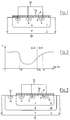
- a MOS capacitor according to a first embodiment of the present invention is shown in cross-section.
- the MOS capacitor comprises an N type well region 1 formed in a P type semiconductor substrate 2. Inside the N type well 1 an N+ contact region 3 is formed to provide a biasing for the N type well, as well as two spaced-apart P+ regions 4. It should be noted that a single P+ region 4 could be sufficient; however, providing more P+ regions 4 properly distributed inside the N type well 1 ensures a better control (minimization) of parasitic resistances.
- an insulated gate is formed comprising an insulating layer 5, typically of SiO 2 , and a conductive layer 6, typically doped polysilicon; the insulated gate substantially covers entirely the N type well 1 with the exception of small contact windows for contacting regions 3 and 4.
- the surface portion of the N type well 1 under the insulated gate forms a channel region.
- the P type substrate 1 is electrically connected to ground; the N+ contact region 3 and the P+ regions 4 form a first electrode of the capacitor, and are electrically connected to a voltage Vc; the conductive layer 6 forms a second electrode of the capacitor and is electrically connected to a voltage Vg.
- Fig. 1 The structure of Fig. 1 is substantially equal to that of a conventional PMOS capacitor (previously described), with the difference that in this case the N+ contact region which provides biasing to the N type well 1 is short-circuited with the P+ regions 4 instead of being connected to an independent voltage supply.
- the N type well 1 can act as an electrode of the capacitor when the latter is operated in accumulation region, i.e. when the voltage (Vg-Vc) is higher than the flat-band voltage Vfb (Fig. 2).
- Vg-Vc the voltage
- Vt threshold voltage
- the presence of the P+ regions 4 improves the behaviour of the capacitor in the inversion region, because they inject holes and it is therefore not necessary to wait for the relatively slow generation-recombiantion process to create the inversion channel under the insulated gate.
- the capacitance is small, approximately one half or one third of its value in the inversion and accumulation regions.
- the voltage Vc should be kept positive, to prevent the N well/P substrate junction to be forward biased.
- Fig. 3 shows in cross-section a MOS capacitor according to a second embodiment of the invention.
- the MOS capacitor comprises an N type well 10 formed in a P type substrate 2, and a P type well 8 formed within the N type well 10.
- a P+ contact region 9 is formed inside the P type well 8, for providing a biasing to the P type well 8, and two spaced-apart N+ regions 11.
- a single N+ region 11 could be sufficient, but better performances are achieved by providing more N+ regions 11.
- an insulated gate is provided comprising the SiO 2 layer 5 and the doped polysilicon layer 6; the surface portion of the P type well 8 under the insulated gate forms a channel region.
- An N+ contact region 13 is further formed inside the N type well 10.
- the N+ regions 11 and the P+ contact region 9 are short-circuited to each other and electrically connected to voltage Vc, and form a first electrode of the MOS capacitor; the polysilicon Layer 6 is electrically connected to voltage Vg and forms a second electrode of the capacitor.
- the N+ contact region 13 is electrically connected to a voltage V1 higher than Vc, to prevent the P well/N well junction from being forward biased.
- the substrate 2 is conventionally kept grounded.
- the MOS capacitor of Fig. 3 is an NMOS capacitor.
- the P type well 8 is short-circuited to the N+ regions 11, so that the P type well 8 can act as an electrode of the capacitor when the latter is operated in the accumulation region.
- the capacitor of Fig. 3 has better frequency performance than that of Fig. 1, because the inversion channel is made up of electrons instead of holes, and it is known that electrons have a higher mobility than holes.
- Fig. 4 shows in cross-section a MOS capacitor according to a third embodiment of the invention.
- the structure is substantially identical to that shown in Fig. 3, with the difference that the insulated gate (i.e., the SiO 2 Layer 5 and the polysilicon layer 6) extends over the N type well 10, and the N+ contact region 13 is electrically connected to voltage Vc.
- This structure is equivalent to the parallel connection of an NMOS capacitor with an N-well capacitor: the NMOS capacitor formed in the P type well 8, and the N-well capacitor formed in the N type well 10.
- One electrode of the capacitor is represented by the polysilicon layer 6, the other electrode is represented by the N+ regions 11, the P type well 8 and the N type well 10 which are short-circuited to each other.
- Fig. 6 shows in cross-section a MOS capacitor according to a fourth embodiment of the present invention.
- This structure is substantially identical to that shown in Fig. 4, except for the fact that the N+ region 13 has been replaced by two N+ regions 131, 132, and a P+ region 14 is provided in the N type well 10 between regions 131 and 132.
- the provision of the P+ region 14 inside the N type well 10 improves the frequency response of the N-well capacitor in the inversion region, because the P+ region 14 supplies holes for the inversion channel. Thanks to this, the capacitance is that shown by curve A', Fig. 5.
- Fig. 7 shows in top-plan view at the level of the surface of the substrate 2 a preferred practical implementation of the MOS capacitor of Fig. 6.
- the N type well 10 has substantially a rectangular shape (square in the shown example), and the P type well 8 has a similar rectangular shape.
- a plurality of N+ diffusions 131 are provided inside the N type well 10, substantially disposed all along the inner perimeter of N type well 10; a plurality of P+ diffusions 14 is also provided, concentrical with the N+ diffusions 131, and, concentrical with the P+ diffusions 14, a plurality of N+ diffusions 132 is provided.
- a plurality of P+ diffusions 9 is provided all along the perimeter of the P type well 8, and two concentrical pluralities of N+ diffusions 11 are also provided; substantially at the center of the P type well 8, a further P+ diffusion 9 is also provided.
- the insulated gate layer covers the whole surface of the N type and P type wells 10 and 8; to each diffusion 131, 14, 132, 9 and 11 corresponds a respective opening in the insulated gate layer to allow the underlying diffusion to be contacted by a metallization layer (not shown).
Landscapes
- Semiconductor Integrated Circuits (AREA)
Priority Applications (3)
| Application Number | Priority Date | Filing Date | Title |
|---|---|---|---|
| EP96830420A EP0822601B1 (fr) | 1996-07-30 | 1996-07-30 | Capacité MOS à larges plages de fonctionnement en tension et en fréquence |
| DE69636161T DE69636161D1 (de) | 1996-07-30 | 1996-07-30 | MOS-Kapazität mit breiten Spannungs- und Frequenzbetriebsbereichen |
| US09/916,954 US6590247B2 (en) | 1996-07-30 | 2001-07-27 | MOS capacitor with wide voltage and frequency operating ranges |
Applications Claiming Priority (1)
| Application Number | Priority Date | Filing Date | Title |
|---|---|---|---|
| EP96830420A EP0822601B1 (fr) | 1996-07-30 | 1996-07-30 | Capacité MOS à larges plages de fonctionnement en tension et en fréquence |
Publications (2)
| Publication Number | Publication Date |
|---|---|
| EP0822601A1 true EP0822601A1 (fr) | 1998-02-04 |
| EP0822601B1 EP0822601B1 (fr) | 2006-05-24 |
Family
ID=8225974
Family Applications (1)
| Application Number | Title | Priority Date | Filing Date |
|---|---|---|---|
| EP96830420A Expired - Lifetime EP0822601B1 (fr) | 1996-07-30 | 1996-07-30 | Capacité MOS à larges plages de fonctionnement en tension et en fréquence |
Country Status (3)
| Country | Link |
|---|---|
| US (1) | US6590247B2 (fr) |
| EP (1) | EP0822601B1 (fr) |
| DE (1) | DE69636161D1 (fr) |
Cited By (2)
| Publication number | Priority date | Publication date | Assignee | Title |
|---|---|---|---|---|
| EP1553636A4 (fr) * | 2003-03-03 | 2006-08-30 | Fujitsu Ltd | Dispositif capacitif a mos variable |
| CN102997944A (zh) * | 2011-09-08 | 2013-03-27 | 飞思卡尔半导体公司 | 入射电容式传感器 |
Families Citing this family (13)
| Publication number | Priority date | Publication date | Assignee | Title |
|---|---|---|---|---|
| US20030058022A1 (en) * | 1999-12-14 | 2003-03-27 | Rajendran Nair | Device and method for controlling voltage variation |
| US6828654B2 (en) * | 2001-12-27 | 2004-12-07 | Broadcom Corporation | Thick oxide P-gate NMOS capacitor for use in a phase-locked loop circuit and method of making same |
| US20040206999A1 (en) * | 2002-05-09 | 2004-10-21 | Impinj, Inc., A Delaware Corporation | Metal dielectric semiconductor floating gate variable capacitor |
| US6825089B1 (en) * | 2003-06-04 | 2004-11-30 | Agere Systems Inc. | Increased quality factor of a varactor in an integrated circuit via a high conductive region in a well |
| JP2007096036A (ja) * | 2005-09-29 | 2007-04-12 | Matsushita Electric Ind Co Ltd | 昇圧回路 |
| TWI405414B (zh) * | 2006-07-11 | 2013-08-11 | Jinnshyan Wang | 差分式高速動態相位偵測器 |
| US20080061838A1 (en) * | 2006-09-11 | 2008-03-13 | Jinn-Shyan Wang | Differential-type high-speed phase detector |
| EP2383781A1 (fr) | 2010-04-19 | 2011-11-02 | Dialog Semiconductor B.V. | Structure de condensateur MOS doté d'une courbe capacité-tension linéaire |
| US8933711B2 (en) | 2011-09-08 | 2015-01-13 | Freescale Semiconductor, Inc. | Capacitive sensor radiation measurement |
| US9318485B2 (en) * | 2012-08-10 | 2016-04-19 | Infineon Technologies Ag | Capacitor arrangements and method for manufacturing a capacitor arrangement |
| US9711516B2 (en) * | 2015-10-30 | 2017-07-18 | Taiwan Semiconductor Manufacturing Company Ltd. | Non-volatile memory having a gate-layered triple well structure |
| TWI662713B (zh) * | 2017-10-05 | 2019-06-11 | 世界先進積體電路股份有限公司 | 半導體裝置以及其製造方法 |
| US10680120B2 (en) | 2018-04-05 | 2020-06-09 | Vanguard International Semiconductor Corporation | Semiconductor device and method for manufacturing the same |
Citations (6)
| Publication number | Priority date | Publication date | Assignee | Title |
|---|---|---|---|---|
| US4167018A (en) * | 1976-02-25 | 1979-09-04 | Hitachi, Ltd. | MIS capacitance element |
| EP0031107A1 (fr) * | 1979-12-15 | 1981-07-01 | Kabushiki Kaisha Toshiba | Procédé de fabrication d'un circuit intégré bipolaire |
| JPS58159367A (ja) * | 1982-03-17 | 1983-09-21 | Matsushita Electronics Corp | Mos容量装置 |
| US4704625A (en) * | 1982-08-05 | 1987-11-03 | Motorola, Inc. | Capacitor with reduced voltage variability |
| EP0464453A1 (fr) * | 1990-06-18 | 1992-01-08 | Kabushiki Kaisha Toshiba | Condensateur de type MIS ayant un changement de capacitance réduit lors de polarisations selon des directions directes et inverses |
| JPH04112564A (ja) * | 1990-08-31 | 1992-04-14 | Nec Ic Microcomput Syst Ltd | 半導体装置 |
Family Cites Families (6)
| Publication number | Priority date | Publication date | Assignee | Title |
|---|---|---|---|---|
| US3612964A (en) | 1969-01-06 | 1971-10-12 | Mitsubishi Electric Corp | Mis-type variable capacitance semiconductor device |
| US4001869A (en) | 1975-06-09 | 1977-01-04 | Sprague Electric Company | Mos-capacitor for integrated circuits |
| JPS5819143B2 (ja) | 1977-09-30 | 1983-04-16 | 株式会社東芝 | 半導体メモリ装置 |
| KR950009815B1 (ko) | 1991-12-23 | 1995-08-28 | 삼성전자주식회사 | 트리플웰 구조를 가지는 고집적 반도체 메모리 장치 |
| US5341009A (en) * | 1993-07-09 | 1994-08-23 | Harris Corporation | Fast charging MOS capacitor structure for high magnitude voltage of either positive or negative polarity |
| JP3510335B2 (ja) | 1994-07-18 | 2004-03-29 | 株式会社ルネサステクノロジ | 半導体記憶装置、内部電源電圧発生回路、内部高電圧発生回路、中間電圧発生回路、定電流源、および基準電圧発生回路 |
-
1996
- 1996-07-30 DE DE69636161T patent/DE69636161D1/de not_active Expired - Lifetime
- 1996-07-30 EP EP96830420A patent/EP0822601B1/fr not_active Expired - Lifetime
-
2001
- 2001-07-27 US US09/916,954 patent/US6590247B2/en not_active Expired - Fee Related
Patent Citations (6)
| Publication number | Priority date | Publication date | Assignee | Title |
|---|---|---|---|---|
| US4167018A (en) * | 1976-02-25 | 1979-09-04 | Hitachi, Ltd. | MIS capacitance element |
| EP0031107A1 (fr) * | 1979-12-15 | 1981-07-01 | Kabushiki Kaisha Toshiba | Procédé de fabrication d'un circuit intégré bipolaire |
| JPS58159367A (ja) * | 1982-03-17 | 1983-09-21 | Matsushita Electronics Corp | Mos容量装置 |
| US4704625A (en) * | 1982-08-05 | 1987-11-03 | Motorola, Inc. | Capacitor with reduced voltage variability |
| EP0464453A1 (fr) * | 1990-06-18 | 1992-01-08 | Kabushiki Kaisha Toshiba | Condensateur de type MIS ayant un changement de capacitance réduit lors de polarisations selon des directions directes et inverses |
| JPH04112564A (ja) * | 1990-08-31 | 1992-04-14 | Nec Ic Microcomput Syst Ltd | 半導体装置 |
Non-Patent Citations (2)
| Title |
|---|
| PATENT ABSTRACTS OF JAPAN vol. 16, no. 360 (E - 1243) 4 August 1992 (1992-08-04) * |
| PATENT ABSTRACTS OF JAPAN vol. 7, no. 280 (E - 216) 14 December 1983 (1983-12-14) * |
Cited By (4)
| Publication number | Priority date | Publication date | Assignee | Title |
|---|---|---|---|---|
| EP1553636A4 (fr) * | 2003-03-03 | 2006-08-30 | Fujitsu Ltd | Dispositif capacitif a mos variable |
| US7622760B2 (en) | 2003-03-03 | 2009-11-24 | Fujitsu Microelectronics Limited | MOS type variable capacitance device |
| CN102997944A (zh) * | 2011-09-08 | 2013-03-27 | 飞思卡尔半导体公司 | 入射电容式传感器 |
| CN102997944B (zh) * | 2011-09-08 | 2016-11-23 | 飞思卡尔半导体公司 | 入射电容式传感器 |
Also Published As
| Publication number | Publication date |
|---|---|
| DE69636161D1 (de) | 2006-06-29 |
| US20010042879A1 (en) | 2001-11-22 |
| US6590247B2 (en) | 2003-07-08 |
| EP0822601B1 (fr) | 2006-05-24 |
Similar Documents
| Publication | Publication Date | Title |
|---|---|---|
| US6828638B2 (en) | Decoupling capacitors for thin gate oxides | |
| US7071507B2 (en) | High-voltage CMOS-compatible capacitors | |
| US6175264B1 (en) | Charge pump for generating negative voltage without change of threshold due to undesirable back-gate biasing effect | |
| EP0822601B1 (fr) | Capacité MOS à larges plages de fonctionnement en tension et en fréquence | |
| US20040021166A1 (en) | Pseudo-nonvolatile direct-tunneling floating-gate device | |
| EP0452829A2 (fr) | Dispositif semi-conducteur avec des défaillances dépendantes du temps diélectriques réduites | |
| US20100226166A1 (en) | MOS capacitor and charge pump with MOS capacitor | |
| KR960012249B1 (ko) | 래치업 방지회로를 가진 cmos 집적회로장치 | |
| US9368506B2 (en) | Integrated circuits and methods for operating integrated circuits with non-volatile memory | |
| JP2002164544A (ja) | 半導体装置 | |
| US6844596B2 (en) | Si-MOS high-frequency semiconductor device | |
| EP1553636B1 (fr) | Dispositif capacitif a mos variable | |
| GB2395065A (en) | Floating gate transistors | |
| EP0263287A2 (fr) | Fabrication d'un capaciteur dans un circuit intégré | |
| US4704625A (en) | Capacitor with reduced voltage variability | |
| US5309009A (en) | Integrated electrically adjustable analog transistor device | |
| KR100883282B1 (ko) | Eeprom | |
| US6771112B1 (en) | Semiconductor integrated circuit having pads with less input signal attenuation | |
| US7491605B2 (en) | Zero cost non-volatile memory cell with write and erase features | |
| JP2000057790A (ja) | 電圧発生回路 | |
| JP2567831B2 (ja) | 電荷検出回路 | |
| JPH0745789A (ja) | 半導体装置のmos容量 | |
| US7388401B2 (en) | Input/output circuit device | |
| JPH1012743A (ja) | インバータ | |
| KR20080100050A (ko) | 반도체 장치의 저장 캐패시터 |
Legal Events
| Date | Code | Title | Description |
|---|---|---|---|
| PUAI | Public reference made under article 153(3) epc to a published international application that has entered the european phase |
Free format text: ORIGINAL CODE: 0009012 |
|
| AK | Designated contracting states |
Kind code of ref document: A1 Designated state(s): DE FR GB IT |
|
| RAP3 | Party data changed (applicant data changed or rights of an application transferred) |
Owner name: STMICROELECTRONICS S.R.L. |
|
| 17P | Request for examination filed |
Effective date: 19980715 |
|
| AKX | Designation fees paid |
Free format text: DE FR GB IT |
|
| RBV | Designated contracting states (corrected) |
Designated state(s): DE FR GB IT |
|
| 17Q | First examination report despatched |
Effective date: 20030723 |
|
| GRAP | Despatch of communication of intention to grant a patent |
Free format text: ORIGINAL CODE: EPIDOSNIGR1 |
|
| GRAJ | Information related to disapproval of communication of intention to grant by the applicant or resumption of examination proceedings by the epo deleted |
Free format text: ORIGINAL CODE: EPIDOSDIGR1 |
|
| GRAP | Despatch of communication of intention to grant a patent |
Free format text: ORIGINAL CODE: EPIDOSNIGR1 |
|
| GRAS | Grant fee paid |
Free format text: ORIGINAL CODE: EPIDOSNIGR3 |
|
| GRAA | (expected) grant |
Free format text: ORIGINAL CODE: 0009210 |
|
| AK | Designated contracting states |
Kind code of ref document: B1 Designated state(s): DE FR GB IT |
|
| REG | Reference to a national code |
Ref country code: GB Ref legal event code: FG4D |
|
| REF | Corresponds to: |
Ref document number: 69636161 Country of ref document: DE Date of ref document: 20060629 Kind code of ref document: P |
|
| PGFP | Annual fee paid to national office [announced via postgrant information from national office to epo] |
Ref country code: IT Payment date: 20060731 Year of fee payment: 11 |
|
| PG25 | Lapsed in a contracting state [announced via postgrant information from national office to epo] |
Ref country code: DE Free format text: LAPSE BECAUSE OF FAILURE TO SUBMIT A TRANSLATION OF THE DESCRIPTION OR TO PAY THE FEE WITHIN THE PRESCRIBED TIME-LIMIT Effective date: 20060825 |
|
| PLBE | No opposition filed within time limit |
Free format text: ORIGINAL CODE: 0009261 |
|
| STAA | Information on the status of an ep patent application or granted ep patent |
Free format text: STATUS: NO OPPOSITION FILED WITHIN TIME LIMIT |
|
| 26N | No opposition filed |
Effective date: 20070227 |
|
| EN | Fr: translation not filed | ||
| PG25 | Lapsed in a contracting state [announced via postgrant information from national office to epo] |
Ref country code: FR Free format text: LAPSE BECAUSE OF FAILURE TO SUBMIT A TRANSLATION OF THE DESCRIPTION OR TO PAY THE FEE WITHIN THE PRESCRIBED TIME-LIMIT Effective date: 20070309 |
|
| PG25 | Lapsed in a contracting state [announced via postgrant information from national office to epo] |
Ref country code: FR Free format text: LAPSE BECAUSE OF FAILURE TO SUBMIT A TRANSLATION OF THE DESCRIPTION OR TO PAY THE FEE WITHIN THE PRESCRIBED TIME-LIMIT Effective date: 20060524 |
|
| PGFP | Annual fee paid to national office [announced via postgrant information from national office to epo] |
Ref country code: GB Payment date: 20080630 Year of fee payment: 13 |
|
| PG25 | Lapsed in a contracting state [announced via postgrant information from national office to epo] |
Ref country code: IT Free format text: LAPSE BECAUSE OF NON-PAYMENT OF DUE FEES Effective date: 20070730 |
|
| GBPC | Gb: european patent ceased through non-payment of renewal fee |
Effective date: 20090730 |
|
| PG25 | Lapsed in a contracting state [announced via postgrant information from national office to epo] |
Ref country code: GB Free format text: LAPSE BECAUSE OF NON-PAYMENT OF DUE FEES Effective date: 20090730 |