EP0823067B1 - Affichages electro-optiques - Google Patents
Affichages electro-optiques Download PDFInfo
- Publication number
- EP0823067B1 EP0823067B1 EP96912099A EP96912099A EP0823067B1 EP 0823067 B1 EP0823067 B1 EP 0823067B1 EP 96912099 A EP96912099 A EP 96912099A EP 96912099 A EP96912099 A EP 96912099A EP 0823067 B1 EP0823067 B1 EP 0823067B1
- Authority
- EP
- European Patent Office
- Prior art keywords
- pixel
- row
- column
- electrode means
- row electrode
- Prior art date
- Legal status (The legal status is an assumption and is not a legal conclusion. Google has not performed a legal analysis and makes no representation as to the accuracy of the status listed.)
- Expired - Lifetime
Links
- 230000003287 optical effect Effects 0.000 claims abstract description 10
- 230000005684 electric field Effects 0.000 claims abstract description 8
- 239000000382 optic material Substances 0.000 claims abstract description 6
- 239000000758 substrate Substances 0.000 claims description 12
- 230000008878 coupling Effects 0.000 claims description 3
- 238000010168 coupling process Methods 0.000 claims description 3
- 238000005859 coupling reaction Methods 0.000 claims description 3
- 239000000463 material Substances 0.000 abstract description 9
- 239000002131 composite material Substances 0.000 description 19
- 229910052751 metal Inorganic materials 0.000 description 6
- 239000002184 metal Substances 0.000 description 6
- 238000000034 method Methods 0.000 description 6
- 230000000694 effects Effects 0.000 description 4
- 239000011159 matrix material Substances 0.000 description 4
- 239000004973 liquid crystal related substance Substances 0.000 description 3
- 229920000642 polymer Polymers 0.000 description 3
- 239000004986 Cholesteric liquid crystals (ChLC) Substances 0.000 description 2
- 150000001875 compounds Chemical class 0.000 description 2
- 238000005516 engineering process Methods 0.000 description 2
- 239000005262 ferroelectric liquid crystals (FLCs) Substances 0.000 description 2
- 239000011521 glass Substances 0.000 description 2
- 229910001111 Fine metal Inorganic materials 0.000 description 1
- 239000004988 Nematic liquid crystal Substances 0.000 description 1
- 230000004888 barrier function Effects 0.000 description 1
- 238000010276 construction Methods 0.000 description 1
- 230000001419 dependent effect Effects 0.000 description 1
- 238000009499 grossing Methods 0.000 description 1
- AMGQUBHHOARCQH-UHFFFAOYSA-N indium;oxotin Chemical compound [In].[Sn]=O AMGQUBHHOARCQH-UHFFFAOYSA-N 0.000 description 1
- 229920000307 polymer substrate Polymers 0.000 description 1
- 238000009877 rendering Methods 0.000 description 1
Images


Classifications
-
- G—PHYSICS
- G02—OPTICS
- G02F—OPTICAL DEVICES OR ARRANGEMENTS FOR THE CONTROL OF LIGHT BY MODIFICATION OF THE OPTICAL PROPERTIES OF THE MEDIA OF THE ELEMENTS INVOLVED THEREIN; NON-LINEAR OPTICS; FREQUENCY-CHANGING OF LIGHT; OPTICAL LOGIC ELEMENTS; OPTICAL ANALOGUE/DIGITAL CONVERTERS
- G02F1/00—Devices or arrangements for the control of the intensity, colour, phase, polarisation or direction of light arriving from an independent light source, e.g. switching, gating or modulating; Non-linear optics
- G02F1/01—Devices or arrangements for the control of the intensity, colour, phase, polarisation or direction of light arriving from an independent light source, e.g. switching, gating or modulating; Non-linear optics for the control of the intensity, phase, polarisation or colour
- G02F1/13—Devices or arrangements for the control of the intensity, colour, phase, polarisation or direction of light arriving from an independent light source, e.g. switching, gating or modulating; Non-linear optics for the control of the intensity, phase, polarisation or colour based on liquid crystals, e.g. single liquid crystal display cells
- G02F1/133—Constructional arrangements; Operation of liquid crystal cells; Circuit arrangements
- G02F1/1333—Constructional arrangements; Manufacturing methods
- G02F1/1343—Electrodes
- G02F1/13439—Electrodes characterised by their electrical, optical, physical properties; materials therefor; method of making
-
- G—PHYSICS
- G02—OPTICS
- G02F—OPTICAL DEVICES OR ARRANGEMENTS FOR THE CONTROL OF LIGHT BY MODIFICATION OF THE OPTICAL PROPERTIES OF THE MEDIA OF THE ELEMENTS INVOLVED THEREIN; NON-LINEAR OPTICS; FREQUENCY-CHANGING OF LIGHT; OPTICAL LOGIC ELEMENTS; OPTICAL ANALOGUE/DIGITAL CONVERTERS
- G02F1/00—Devices or arrangements for the control of the intensity, colour, phase, polarisation or direction of light arriving from an independent light source, e.g. switching, gating or modulating; Non-linear optics
- G02F1/01—Devices or arrangements for the control of the intensity, colour, phase, polarisation or direction of light arriving from an independent light source, e.g. switching, gating or modulating; Non-linear optics for the control of the intensity, phase, polarisation or colour
- G02F1/13—Devices or arrangements for the control of the intensity, colour, phase, polarisation or direction of light arriving from an independent light source, e.g. switching, gating or modulating; Non-linear optics for the control of the intensity, phase, polarisation or colour based on liquid crystals, e.g. single liquid crystal display cells
- G02F1/133—Constructional arrangements; Operation of liquid crystal cells; Circuit arrangements
- G02F1/1333—Constructional arrangements; Manufacturing methods
- G02F1/1343—Electrodes
- G02F1/134309—Electrodes characterised by their geometrical arrangement
- G02F1/134336—Matrix
-
- G—PHYSICS
- G02—OPTICS
- G02F—OPTICAL DEVICES OR ARRANGEMENTS FOR THE CONTROL OF LIGHT BY MODIFICATION OF THE OPTICAL PROPERTIES OF THE MEDIA OF THE ELEMENTS INVOLVED THEREIN; NON-LINEAR OPTICS; FREQUENCY-CHANGING OF LIGHT; OPTICAL LOGIC ELEMENTS; OPTICAL ANALOGUE/DIGITAL CONVERTERS
- G02F2203/00—Function characteristic
- G02F2203/30—Gray scale
Definitions
- This invention relates to electro-optic displays.
- TN LCDs Twisted Nematic Liquid Crystal Displays
- cathode ray tubes etc.
- TN LCDs Twisted Nematic Liquid Crystal Displays
- the intensity of each pixel may be selected in proportion to the area of the pixel that should be ON. Whilst this can reduce the visually disturbing staircase effect, it can make edges in the displayed image appear blurred, especially when viewed from close to the display.
- the image to be displayed is analysed and two-bit pixel data is added to each pixel to turn on selected sub pixel slices during a pixel sub-scanning period.
- This allows a range of intensities to be displayed by varying the area of the pixel that is ON, in four discrete steps.
- this system is only capable of modulating the pixel output slice-wise and in many instances this will not give good smoothing, particularly where the edge to be smoothed is nearly perpendicular to the slice direction of the pixels.
- EP-A-462 619 discloses an optical modulation element capable of displaying gradations comprising a plurality of two or more electrodes in a "Y" direction, a plurality of subelectrodes in the same direction and a plurality of segment electrodes in an "X" direction, facing the Y electrodes and subelectrodes.
- this invention provides a display as defined in claim 1.
- the multiple track architecture for each of the row and column electrodes provides important and unexpected advantages when used in conjunction with drive means which apply a selected voltage profile across each of the groups of tracks making up an electrode.
- the magnitude of the electrical field across the pixel may be varied in a direction transverse to the thickness of the electro-optic layer to provide a non-uniform optical output across the pixel.
- the multiple conductive tracks of the present invention may be driven by electrical contacts well away from the image area, thus considerably improving the aperture ratio of the display.
- the resistive elements may be formed on the first and second substrates, in electrical contact with the respective conductive tracks.
- the row and column resistive elements may be formed on separate substrates which are then placed in contact with the first and second substrates.
- the series of resistive elements driving the groups of conductive tracks may be replaced by a single resistive element in electrical contact with a substantial proportion of, or all the conductive tracks making up the complete set of row/column electrodes, with the drive means including an input electrode means between each group of conductive tracks.
- said drive means includes means for applying an adjustable voltage across each of said resistive elements, so that the voltage profile across the group of conductive tracks is a ramp of positive, negative or zero slope.
- the drives to the groups of tracks may be inductively or capacitively coupled.
- the electrical field may be configured to generate a wide range of different non-uniform outputs of selected shape for a pixel, to turn on an arbitrary portion of the pixel, so that the required edge of the line portion of the text character etc is maintained within the area of the pixel.
- each of a set of predetermined voltage profiles is applied across a row electrode means in successive phases, and the columns driven in parallel with the required voltage profiles.
- a broad range of pixel shapes may be provided in either a single write (i.e. just one of the phases) or a multiple write where the pixel output is incrementally rendered. It will be appreciated that this drive scheme could be modified so that the multiple successive phases are applied to the columns whilst the rows are driven in parallel.
- the electro-optic material may have a steep or "fast" electro-optic curve, i.e. where the electro-optic effect switches state abruptly at a particular threshold voltage, so that the optical output at a particular point within the pixel will vary between two generally discrete levels, dependent on whether the field strength at that point is above or below the threshold voltage.
- the boundary between ON and OFF regions in the pixel will be determined by an equi-potential line on the notional voltage surface within the pixel of magnitude corresponding to said threshold voltage.
- the electro-optic material may have a shallow or "slow" electro-optic curve, with the output varying continuously between ON and OFF through grey levels, so that the optical output may be shaded across the pixel, generally in accordance with the magnitude of the electrical field.
- the image to be displayed is analysed to determine those pixels where some form of intra-pixel variation is required, for example where the pixel is lying on an edge of the image or where grey-scaling or half toning is required.
- the display driver determines the desired boundary lines between ON and OFF, and the electrical field intensity required, and then selects suitable voltages to be applied to the pixel to generate the required variation or level of electrical field across the pixel.
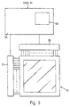
- the display 10 comprises a lower glass or polymer substrate 11 on which a series of electrically conductive tracks 12 is formed, for example from a high conductivity Indium Tin Oxide (ITO) layer.
- ITO Indium Tin Oxide
- the conductive tracks 12 are connected together in groups of four by a resistive pad 13 to one side of the display, each group defining a composite row electrode 14.
- a selected voltage ramp may be applied across the resistive pad 13 by means of input electrodes 15.
- the voltage applied to each electrode is independently selectable to allow a range of voltage profiles to be applied.
- the effect of applying a voltage ramp across the resistive pad is to set each of the conductive tracks 12 making up the composite electrode to a predetermined adjustable voltage and effectively to set up a potential gradient across the lower surface of each of the pixels contained in the row, in the plane of the electrode.
- a polymer alignment layer (not shown) overlies the conductive tracks and serves to align the adjacent liquid crystal layer 16.
- a further polymer alignment layer and a set of composite column electrodes 17 Adjacent the upper surface of the liquid crystal layer 16 there is provided a further polymer alignment layer and a set of composite column electrodes 17 each comprising a group of conductive tracks 18 interconnected by resistive pads 19, and similar in construction and grouping to the row electrodes.
- a voltage ramp may be applied across the column electrode by means of input electrodes 20 at opposite ends of each of the resistive pads.
- a pixel 22 is defined at each crossing of a composite row electrode 14 by a composite column electrode 17.
- the illustrated arrangement allows the orthogonal voltage profiles across the upper and lower surfaces bounding a pixel to be independently adjusted to apply a compound voltage profile to the pixel.
- the optical output at a particular point in the pixel will depend on whether the compound voltage at that point is or, for some materials, has been above the threshold voltage for that material. In this way a variety of complex geometrical shapes may be written within the pixel by suitable control of the voltage ramps applied to the relevant composite row and column electrodes.
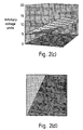
- FIG. 2(a) shows the voltage profile applied across the lower surface of the pixel by means of the relevant composite row electrode 14, by applying 10 voltage units to the upper row input electrode 15' and 15 voltage units to the lower row input electrode 15".
- Figure 2(b) shows the voltage profile applied to the upper surface by means of the composite column electrode 17, by applying 10 voltage units to the left column electrode 20' and 0 voltage units to the right column electrode 20".
- Figure 2(c) shows the resultant field across the pixel corresponding to the difference between the two voltage surfaces
- Figure 2(d) gives the resultant optical output.
- the dividing line may not be straight but this is unlikely to be perceptible.
- the resolution may be improved by increasing the number of electrodes in a group.
- a wide range of sub pixel shapes may thus be generated by suitable selection of the adjustable voltages (four in all) applied to the top/bottom input electrodes of the resistive pad 13 on the relevant composite row electrode 14,and the left/right input electrodes of the resistive patch on the relevant composite column electrode 17. It should be noted that selected sub portions of the pixel may be set or unset as required.
- a modified electrode structure is shown in Figure 3.
- a single resistive pad 26 is in electrical contact with the resistive tracks 12 making up a number of composite row electrodes, and may interconnect with all the row tracks 12.
- an input electrode 28 Between each group of tracks making up the electrode is an input electrode 28 so that the required voltage ramps may be set up across each of the composite row electrodes either singly, or in combination with a number of adjacent rows.
- the whole, or a variable sized portion of the display may be driven, e.g. by driving the upper electrode of the first row and the lower electrode of the last row.
- the first scheme is for a LCD material such as Ferroelectric LCD and similar materials which can be selectively set and unset.
- a blanking or erasure pulse is applied to a composite row electrode 14 to clear the pixels in the row.
- the row is then written by a multi-phase write, in which a finite set of voltage ramps is applied across the upper and lower input electrodes 15', 15" on the resistive pad, for example "High” (both set high), “Low” (both set low), positive slope (upper set high, lower set low) and negative slope (upper set low, lower set high).
- the composite column electrodes 17 that would require that particular "vertical" ramp on their lower surface have the appropriate respective horizontal ramps set on each of the input electrodes 20', 20" on each of the column resistive pads 19.
- This allows complex shape pixels to be set up as the union or difference of the primitive shapes set up by any particular combination of row/column ramps.
- the maximum amplitude of the two ramps is set below half the threshold voltage of the material to prevent cross talk.
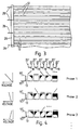
- Figure 4 shows how the shapes in the pixels in a given row may be built up in successive phases. Thus in phase 1 a steep positive ramp is applied to the composite row electrode 14.
- a positive ramp is applied to the first pixel, a low ramp is applied to the second, a negative slope to the third and fourth, and a high is applied to the fifth, to give the first phase results as shown.
- a gentle positive slope is applied to the composite row electrode 14.
- low ramps are applied to the first, third and fourth pixels (resulting in no change), a negative slope is applied to the second pixel and a positive slope applied to the fourth. This writes part of the second pixel and modifies the fifth pixel.
- a gentle negative slope is applied to the composite row electrode.
- low ramps are applied to the first second and fifth pixels, a positive slope is applied to the third pixel and a high slope applied to the fourth pixel.
- the display may be written with all the phases for a row completed before the next row is selected, as suggested by Figure 4, or each phase may be written on a row by row basis, or a variety of interleaving schemes could be used, to maximise clarity and immediacy of the information displayed.
- the image data to be presented on the display 10 is processed using known processing techniques to determine the boundary pixels at the edge of text or images etc, where jagged edges would be visually unacceptable.
- the image processor 24 incorporates a look up table 26 which indicates the pixel shapes obtainable and the voltage ramps required to produce these shapes. The image processor 24 then selects the appropriate voltage ramps for the driving phases to match the shapes required and controls the row and column drives 27, 28 accordingly.
- TN Passive Matrix Twisted Nematic
- STN Passive Matrix Supertwist Nematic
- Active Matrix TN LCDs Stabilised Cholesteric Liquid Crystal Devices, Passive Matrix Ferroelectric and Field Emissive Devices.
Landscapes
- Physics & Mathematics (AREA)
- Nonlinear Science (AREA)
- Mathematical Physics (AREA)
- Chemical & Material Sciences (AREA)
- Crystallography & Structural Chemistry (AREA)
- General Physics & Mathematics (AREA)
- Optics & Photonics (AREA)
- Liquid Crystal (AREA)
- Liquid Crystal Display Device Control (AREA)
- Control Of Indicators Other Than Cathode Ray Tubes (AREA)
Abstract
Claims (9)
- Affichage (10) pour afficher une image, ledit affichage comprenant :un premier substrat (11) ayant sur lui une pluralité de moyens d'électrode de rangée (14), chacun comprenant une pluralité de pistes conductrices électriquement (12),un second substrat ayant sur lui une pluralité de moyens d'électrode de colonne (17), chacun comprenant une pluralité de pistes conductrices électriquement (18),une couche (16) d'un matériau à base électro-optique disposée entre ledit premier (11) et ledit second substrat pour définir de cette façon un pixel (22) entre chacun du croisement d'un moyen d'électrode de rangée (14) avec un moyen d'électrode de colonne (18),des moyens de commande de rangée (13, 15) associé audit premier substrat arrangé de manière à appliquer un profil de tension sélectionné respectif aux bornes de chaque moyen d'électrode de rangée dans une direction transverse à l'épaisseur de ladite couche (16) et à traverser la direction longitudinale desdites pistes dudit moyen d'électrode de rangée,des moyens de commande de colonne (19, 20) associés audit second substrat arrangé de manière à appliquer un profil de tension sélectionné respectif aux bornes de chaque moyen d'électrode de colonne (17) dans une direction transverse à l'épaisseur de ladite couche (16) et transverse à la direction longitudinale desdites pistes desdits moyens d'électrode de colonne,avec pour effet que le champ électrique dans chaque pixel (22) dans la direction transverse à l'épaisseur de la couche électro-optique peut être sélectionné pour fournir une sortie optique non uniforme aux bornes dudit pixel (22), etdes moyens (24) pour commander les profils de tension appliqués par lesdits moyens de commande de rangée (13, 15) et lesdits moyens de commande de colonne (19, 20) pour fournir des pixels sélectionnés (22) avec une sortie de pixel non uniforme prédéterminée dans laquelle la frontière entre la région excitée et la région désexcitée à l'intérieur du pixel est sélectionnée en conformité avec la région correspondante de l'image à afficher.
- Affichage selon la revendication 1, dans lequel chacun desdits moyens d'électrode de rangée (14) inclut un moyen d'impédance (13) couplant entre elles les pistes conductrices électriquement (12) conciliant lesdits moyens d'électrode de rangée, et chacun desdits moyens d'électrode de colonne (17) inclut des moyens d'impédance (19) couplant ensemble les pistes conductrices électriquement (18) constituant lesdits moyens d'électrode de colonne.
- Affichage selon la revendication 2, dans lequel chacun desdits moyens d'impédance (13 ; 19) comprend un élément résistif électriquement en contact chacun avec lesdites pistes conductrices électriquement (12 ; 18).
- Affichage selon la revendication 2 ou 3, incluant des moyens (15 ; 20) pour appliquer une rampe de tension ajustable sélectionnée aux bornes des régions d'extrémité opposée de chacun desdits moyens d'impédance (13 ; 19).
- Affichage selon l'une quelconque des revendications 2 à 4, dans lequel les moyens d'impédance d'électrode de rangée (13) sont fournis sur ledit premier substrat (11) et les moyens d'impédance d'électrode de commande (19) sont fournis sur ledit second substrat.
- Affichage selon l'une quelconque des revendications 2 à 4, dans lequel les moyens d'impédance d'électrode de rangée et lesdits moyens d'impédance d'électrode de colonne (13) sont fournis sur des moyens de substrat autres respectifs (19) disposés en un contact électrique avec lesdits premier et second substrat respectivement.
- Affichage selon la revendication 2 , dans lequel chacun desdits moyens d'impédance (13 ; 19) comprend un élément résistif électriquement (26) étant en contact avec les pistes conductrices (12) d'au moins un de plusieurs moyens d'électrode de rangée, et inclut des moyens d'électrode d'entrée (28) intermédiaires à chacun des moyens d'électrode de rangée.
- Affichage selon la revendication 1, dans lequel lesdits moyens de commande de rangée (13 ; 15) sont inductivement ou de manière capacitive couplés à chacun desdits moyens d'électrode de rangée et dans lequel lesdits moyens de commande de colonne (19, 20) et inductivement ou de manière capacitive couplés à chacun desdits moyens d'électrode de colonne.
- Affichage selon l'une quelconque des revendications précédentes, comprenant des moyens de contrôle d'affichage (24) en réponse aux images d'entrée de données pour amener lesdits moyens de commande de rangée (27) à appliquer à chacun des moyens d'électrode de rangée (14) dans des phases successives, chacun d'une série de profils de tension prédéterminés et pour entraíner desdits moyens de commande de colonne (28) à appliquer auxdits moyens d'électrode de colonne (17) des profils de tension sélectionnés pour créer le pixel non uniforme désiré (22).
Priority Applications (1)
| Application Number | Priority Date | Filing Date | Title |
|---|---|---|---|
| EP96912099A EP0823067B1 (fr) | 1995-04-28 | 1996-04-29 | Affichages electro-optiques |
Applications Claiming Priority (4)
| Application Number | Priority Date | Filing Date | Title |
|---|---|---|---|
| EP95302888A EP0740187B1 (fr) | 1995-04-28 | 1995-04-28 | Afficheur électro-optique |
| EP95302888 | 1995-04-28 | ||
| PCT/GB1996/001009 WO1996034312A1 (fr) | 1995-04-28 | 1996-04-29 | Affichages electro-optiques |
| EP96912099A EP0823067B1 (fr) | 1995-04-28 | 1996-04-29 | Affichages electro-optiques |
Publications (2)
| Publication Number | Publication Date |
|---|---|
| EP0823067A1 EP0823067A1 (fr) | 1998-02-11 |
| EP0823067B1 true EP0823067B1 (fr) | 2002-07-31 |
Family
ID=8221177
Family Applications (2)
| Application Number | Title | Priority Date | Filing Date |
|---|---|---|---|
| EP95302888A Expired - Lifetime EP0740187B1 (fr) | 1995-04-28 | 1995-04-28 | Afficheur électro-optique |
| EP96912099A Expired - Lifetime EP0823067B1 (fr) | 1995-04-28 | 1996-04-29 | Affichages electro-optiques |
Family Applications Before (1)
| Application Number | Title | Priority Date | Filing Date |
|---|---|---|---|
| EP95302888A Expired - Lifetime EP0740187B1 (fr) | 1995-04-28 | 1995-04-28 | Afficheur électro-optique |
Country Status (5)
| Country | Link |
|---|---|
| US (2) | US6295044B1 (fr) |
| EP (2) | EP0740187B1 (fr) |
| JP (1) | JPH11514449A (fr) |
| DE (2) | DE69533187T2 (fr) |
| WO (1) | WO1996034312A1 (fr) |
Families Citing this family (13)
| Publication number | Priority date | Publication date | Assignee | Title |
|---|---|---|---|---|
| EP0740187B1 (fr) * | 1995-04-28 | 2004-06-23 | Hewlett-Packard Company, A Delaware Corporation | Afficheur électro-optique |
| KR100595926B1 (ko) | 1998-01-26 | 2006-07-05 | 웨인 웨스터만 | 수동 입력 통합 방법 및 장치 |
| US6417168B1 (en) | 1998-03-04 | 2002-07-09 | The Trustees Of The University Of Pennsylvania | Compositions and methods of treating tumors |
| US6853360B1 (en) * | 1999-05-04 | 2005-02-08 | Homer L. Webb | Electrode structure for liquid crystal display |
| US6654017B1 (en) * | 2000-04-06 | 2003-11-25 | Sun Microsystems, Inc. | Smoothing of line segments on a computer display |
| GB0109015D0 (en) * | 2001-04-11 | 2001-05-30 | Koninkl Philips Electronics Nv | Bistable chiral nematic liquid crystal display and method of driving the same |
| US8269727B2 (en) | 2007-01-03 | 2012-09-18 | Apple Inc. | Irregular input identification |
| US8130203B2 (en) | 2007-01-03 | 2012-03-06 | Apple Inc. | Multi-touch input discrimination |
| US7855718B2 (en) | 2007-01-03 | 2010-12-21 | Apple Inc. | Multi-touch input discrimination |
| JP2008224759A (ja) * | 2007-03-08 | 2008-09-25 | Seiko Epson Corp | アクティブマトリクス回路基板及び表示装置 |
| KR101219273B1 (ko) * | 2011-01-14 | 2013-01-08 | 삼성디스플레이 주식회사 | 터치 스크린 시스템 |
| US11703698B1 (en) | 2018-08-30 | 2023-07-18 | Apple Inc. | Adjustable lens systems |
| US11880111B1 (en) * | 2020-03-04 | 2024-01-23 | Apple Inc. | Tunable lens systems with voltage selection circuitry |
Family Cites Families (11)
| Publication number | Priority date | Publication date | Assignee | Title |
|---|---|---|---|---|
| FR2499744B1 (fr) * | 1981-01-05 | 1986-07-04 | Commissariat Energie Atomique | Dispositif d'affichage matriciel comprenant deux familles d'electrodes lignes et son procede de commande |
| US4655561A (en) * | 1983-04-19 | 1987-04-07 | Canon Kabushiki Kaisha | Method of driving optical modulation device using ferroelectric liquid crystal |
| US4828370A (en) * | 1985-10-04 | 1989-05-09 | Seiko Instruments & Electronics Ltd. | Switching element with nonlinear resistive, nonstoichiometric material |
| JPS62100739A (ja) * | 1985-10-29 | 1987-05-11 | Matsushita Electric Ind Co Ltd | 液晶表示装置 |
| JPS62119521A (ja) * | 1985-11-19 | 1987-05-30 | Canon Inc | 光学変調装置 |
| US4824218A (en) * | 1986-04-09 | 1989-04-25 | Canon Kabushiki Kaisha | Optical modulation apparatus using ferroelectric liquid crystal and low-resistance portions of column electrodes |
| NL9000942A (nl) * | 1990-04-20 | 1991-11-18 | Philips Nv | Weergeefinrichting. |
| US5225919A (en) * | 1990-06-21 | 1993-07-06 | Matsushita Electric Industrial Co., Ltd. | Optical modulation element including subelectrodes |
| NL9002011A (nl) * | 1990-09-13 | 1992-04-01 | Philips Nv | Weergeefinrichting. |
| GB9324710D0 (en) * | 1993-12-02 | 1994-01-19 | Central Research Lab Ltd | Analogue greyscale addressing |
| EP0740187B1 (fr) * | 1995-04-28 | 2004-06-23 | Hewlett-Packard Company, A Delaware Corporation | Afficheur électro-optique |
-
1995
- 1995-04-28 EP EP95302888A patent/EP0740187B1/fr not_active Expired - Lifetime
- 1995-04-28 DE DE69533187T patent/DE69533187T2/de not_active Expired - Lifetime
-
1996
- 1996-04-29 DE DE69622703T patent/DE69622703T2/de not_active Expired - Lifetime
- 1996-04-29 WO PCT/GB1996/001009 patent/WO1996034312A1/fr not_active Ceased
- 1996-04-29 JP JP8532281A patent/JPH11514449A/ja not_active Ceased
- 1996-04-29 US US08/930,819 patent/US6295044B1/en not_active Expired - Fee Related
- 1996-04-29 EP EP96912099A patent/EP0823067B1/fr not_active Expired - Lifetime
-
2001
- 2001-06-19 US US09/884,258 patent/US6590558B2/en not_active Expired - Fee Related
Also Published As
| Publication number | Publication date |
|---|---|
| WO1996034312A1 (fr) | 1996-10-31 |
| JPH11514449A (ja) | 1999-12-07 |
| DE69622703D1 (de) | 2002-09-05 |
| US6590558B2 (en) | 2003-07-08 |
| EP0740187B1 (fr) | 2004-06-23 |
| EP0740187A1 (fr) | 1996-10-30 |
| US20010030637A1 (en) | 2001-10-18 |
| DE69533187D1 (de) | 2004-07-29 |
| EP0823067A1 (fr) | 1998-02-11 |
| US6295044B1 (en) | 2001-09-25 |
| DE69533187T2 (de) | 2005-07-07 |
| DE69622703T2 (de) | 2002-12-05 |
Similar Documents
| Publication | Publication Date | Title |
|---|---|---|
| EP0361981B1 (fr) | Dispositif d'affichage à cristal liquide pour affichage avec niveaux de gris | |
| US5808705A (en) | Liquid crystal display apparatus with two viewing angle modes and drive electrodes for mode dependent selection | |
| CN100409095C (zh) | 电泳显示装置 | |
| US7724337B2 (en) | In-plane switching LCD apparatus having parallel uniform pixel and common electrode extensions having a principal portion and a specific portion | |
| EP0823067B1 (fr) | Affichages electro-optiques | |
| EP0224243A2 (fr) | Dispositif de modulation optique et procédé de commande de celui-ci | |
| JPH0766248B2 (ja) | 液晶表示装置及びその駆動方法 | |
| JPH06180564A (ja) | 液晶表示装置 | |
| JPS5846454Y2 (ja) | 液晶表示装置の電極構造 | |
| JP3022646B2 (ja) | 表示装置 | |
| JP3363731B2 (ja) | 階調表示可能な表示装置 | |
| KR940006349B1 (ko) | 표시 장치 | |
| JPH0527218A (ja) | 液晶表示装置 | |
| JPH05224177A (ja) | 表示装置 | |
| JPH0812347B2 (ja) | 液晶素子とその駆動法 | |
| JPH08254707A (ja) | ピクセルエレメント | |
| JPH10311989A (ja) | 液晶表示素子 | |
| JPH07281151A (ja) | 液晶表示装置 | |
| JPH07181445A (ja) | 液晶表示装置 | |
| JPH0799415B2 (ja) | 液晶装置 | |
| JPH04276794A (ja) | 液晶表示装置 | |
| KR100325843B1 (ko) | 전계의존효과가감소된단순행렬형액정표시소자 | |
| JPH10232405A (ja) | 階調表示可能な表示装置 | |
| JPH08101392A (ja) | 液晶装置および液晶表示装置 | |
| JP2002148587A (ja) | 液晶表示装置とその駆動方法 |
Legal Events
| Date | Code | Title | Description |
|---|---|---|---|
| PUAI | Public reference made under article 153(3) epc to a published international application that has entered the european phase |
Free format text: ORIGINAL CODE: 0009012 |
|
| 17P | Request for examination filed |
Effective date: 19971022 |
|
| AK | Designated contracting states |
Kind code of ref document: A1 Designated state(s): DE FR GB |
|
| 17Q | First examination report despatched |
Effective date: 19981030 |
|
| RAP1 | Party data changed (applicant data changed or rights of an application transferred) |
Owner name: HEWLETT-PACKARD COMPANY, A DELAWARE CORPORATION |
|
| GRAG | Despatch of communication of intention to grant |
Free format text: ORIGINAL CODE: EPIDOS AGRA |
|
| GRAG | Despatch of communication of intention to grant |
Free format text: ORIGINAL CODE: EPIDOS AGRA |
|
| GRAH | Despatch of communication of intention to grant a patent |
Free format text: ORIGINAL CODE: EPIDOS IGRA |
|
| GRAH | Despatch of communication of intention to grant a patent |
Free format text: ORIGINAL CODE: EPIDOS IGRA |
|
| GRAA | (expected) grant |
Free format text: ORIGINAL CODE: 0009210 |
|
| AK | Designated contracting states |
Kind code of ref document: B1 Designated state(s): DE FR GB |
|
| REG | Reference to a national code |
Ref country code: GB Ref legal event code: FG4D |
|
| REF | Corresponds to: |
Ref document number: 69622703 Country of ref document: DE Date of ref document: 20020905 |
|
| ET | Fr: translation filed | ||
| PLBE | No opposition filed within time limit |
Free format text: ORIGINAL CODE: 0009261 |
|
| STAA | Information on the status of an ep patent application or granted ep patent |
Free format text: STATUS: NO OPPOSITION FILED WITHIN TIME LIMIT |
|
| 26N | No opposition filed |
Effective date: 20030506 |
|
| PGFP | Annual fee paid to national office [announced via postgrant information from national office to epo] |
Ref country code: FR Payment date: 20050418 Year of fee payment: 10 |
|
| REG | Reference to a national code |
Ref country code: FR Ref legal event code: ST Effective date: 20061230 |
|
| PG25 | Lapsed in a contracting state [announced via postgrant information from national office to epo] |
Ref country code: FR Free format text: LAPSE BECAUSE OF NON-PAYMENT OF DUE FEES Effective date: 20060502 |
|
| REG | Reference to a national code |
Ref country code: GB Ref legal event code: 732E Free format text: REGISTERED BETWEEN 20120329 AND 20120404 |
|
| PGFP | Annual fee paid to national office [announced via postgrant information from national office to epo] |
Ref country code: GB Payment date: 20130326 Year of fee payment: 18 |
|
| PGFP | Annual fee paid to national office [announced via postgrant information from national office to epo] |
Ref country code: DE Payment date: 20130322 Year of fee payment: 18 |
|
| REG | Reference to a national code |
Ref country code: DE Ref legal event code: R119 Ref document number: 69622703 Country of ref document: DE |
|
| GBPC | Gb: european patent ceased through non-payment of renewal fee |
Effective date: 20140429 |
|
| PG25 | Lapsed in a contracting state [announced via postgrant information from national office to epo] |
Ref country code: GB Free format text: LAPSE BECAUSE OF NON-PAYMENT OF DUE FEES Effective date: 20140429 Ref country code: DE Free format text: LAPSE BECAUSE OF NON-PAYMENT OF DUE FEES Effective date: 20141101 |
|
| REG | Reference to a national code |
Ref country code: DE Ref legal event code: R119 Ref document number: 69622703 Country of ref document: DE Effective date: 20141101 |