EP0823719B1 - Condensateur électrolytique solide ayant les connexions externes préplaquées, et son procédé de fabrication - Google Patents
Condensateur électrolytique solide ayant les connexions externes préplaquées, et son procédé de fabrication Download PDFInfo
- Publication number
- EP0823719B1 EP0823719B1 EP97112365A EP97112365A EP0823719B1 EP 0823719 B1 EP0823719 B1 EP 0823719B1 EP 97112365 A EP97112365 A EP 97112365A EP 97112365 A EP97112365 A EP 97112365A EP 0823719 B1 EP0823719 B1 EP 0823719B1
- Authority
- EP
- European Patent Office
- Prior art keywords
- plating
- pulse
- lead terminals
- plating layer
- plated
- Prior art date
- Legal status (The legal status is an assumption and is not a legal conclusion. Google has not performed a legal analysis and makes no representation as to the accuracy of the status listed.)
- Expired - Lifetime
Links
Images


Classifications
-
- H—ELECTRICITY
- H01—ELECTRIC ELEMENTS
- H01G—CAPACITORS; CAPACITORS, RECTIFIERS, DETECTORS, SWITCHING DEVICES, LIGHT-SENSITIVE OR TEMPERATURE-SENSITIVE DEVICES OF THE ELECTROLYTIC TYPE
- H01G9/00—Electrolytic capacitors, rectifiers, detectors, switching devices, light-sensitive or temperature-sensitive devices; Processes of their manufacture
- H01G9/004—Details
- H01G9/008—Terminals
-
- H—ELECTRICITY
- H01—ELECTRIC ELEMENTS
- H01G—CAPACITORS; CAPACITORS, RECTIFIERS, DETECTORS, SWITCHING DEVICES, LIGHT-SENSITIVE OR TEMPERATURE-SENSITIVE DEVICES OF THE ELECTROLYTIC TYPE
- H01G9/00—Electrolytic capacitors, rectifiers, detectors, switching devices, light-sensitive or temperature-sensitive devices; Processes of their manufacture
- H01G9/004—Details
- H01G9/008—Terminals
- H01G9/012—Terminals specially adapted for solid capacitors
-
- C—CHEMISTRY; METALLURGY
- C25—ELECTROLYTIC OR ELECTROPHORETIC PROCESSES; APPARATUS THEREFOR
- C25D—PROCESSES FOR THE ELECTROLYTIC OR ELECTROPHORETIC PRODUCTION OF COATINGS; ELECTROFORMING; APPARATUS THEREFOR
- C25D5/00—Electroplating characterised by the process; Pretreatment or after-treatment of workpieces
- C25D5/18—Electroplating using modulated, pulsed or reversing current
-
- H—ELECTRICITY
- H01—ELECTRIC ELEMENTS
- H01G—CAPACITORS; CAPACITORS, RECTIFIERS, DETECTORS, SWITCHING DEVICES, LIGHT-SENSITIVE OR TEMPERATURE-SENSITIVE DEVICES OF THE ELECTROLYTIC TYPE
- H01G9/00—Electrolytic capacitors, rectifiers, detectors, switching devices, light-sensitive or temperature-sensitive devices; Processes of their manufacture
- H01G9/15—Solid electrolytic capacitors
-
- H—ELECTRICITY
- H10—SEMICONDUCTOR DEVICES; ELECTRIC SOLID-STATE DEVICES NOT OTHERWISE PROVIDED FOR
- H10W—GENERIC PACKAGES, INTERCONNECTIONS, CONNECTORS OR OTHER CONSTRUCTIONAL DETAILS OF DEVICES COVERED BY CLASS H10
- H10W90/00—Package configurations
- H10W90/701—Package configurations characterised by the relative positions of pads or connectors relative to package parts
- H10W90/731—Package configurations characterised by the relative positions of pads or connectors relative to package parts of die-attach connectors
- H10W90/736—Package configurations characterised by the relative positions of pads or connectors relative to package parts of die-attach connectors between a chip and a stacked lead frame, conducting package substrate or heat sink
Definitions
- the present invention relates to a resin-molded electronic component having lead terminals, and more particularly, to a chip type solid electrolyte capacitor having solder plated lead terminals, and a process for manufacturing the same.
- the chip type component such as a solid electrolyte capacitor featuring a small size and high capacity has enjoyed an increasingly expanded market scale and is used in various applications.
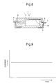
- a chip type solid electrolyte capacitor has a capacitor element 1 having a cathode layer 3, an anode lead 2, an anode lead terminal 8 connected to the anode lead 2 by welding or the like, and a cathode lead terminal 9 connected to the cathode layer 3.
- the cathode layer 3 and the cathode lead terminal 9 are connected by a conductive adhesive 10 such as silver paste.
- the capacitor is packaged by resin 6, leaving portions of the anode and cathode lead terminals 8 and 9 exposed.
- the anode and cathode lead terminals 8 and 9 are bent along the outer surface of the resin package 6. Since these lead terminals 8 and 9 are pre-plated with a plating layer of solder or the like by a direct current plating method using a linear current waveform as shown in Fig.9, it has the following disadvantages (1) and (2).
- Patents Abstracts of Japan, vol. 95, no. 11, & JP 07 202100 A discloses a method of plating lead parts of a semiconductor device, in which alternately positive pulse currents and negative pulse currents having absolute values which are smaller than those of the positive pulse currents are supplied. By this means plated films with nearly constant thickness over the whole lead parts are obtained.
- the above objective of the present invention is achieved by employing electroplated lead terminals which contain organic substances in an amount of 0.03 wt % or less.
- a pre-plated anode lead terminal is welded to an anode lead of a capacitor element and pre-plated cathode lead terminal is connected to a cathode layer of the capacitor element by using a conductive adhesive.
- the capacitor element is encapsulated by an insulating member so as to leave a portion of anode and cathode lead terminals exposed. Both of the encapsulated and exposed portions of the pre-plated anode and cathode lead terminals have a pre-plated layer containing organic substances in an amount of 0.03 wt.% or less.
- Such a small amount of the organic substances in the electroplated layer can be achieved by using a special puls plating method with a current waveform having a counter pulse.
- ON time and OFF time of the current waveform is selected to be about 10 to 500 msec and the OFF time includes a counter (negative) current pulse which has an amplitude that is from 1/2 to 1/50 that of the ON time pulse and a duration of 2 to 20 msec.
- Fig. 1 is a side cross sectional view of a chip type solid electrolyte capacitor according to an embodiment of the present invention.
- Fig. 2A is a perspective view of a chip type solid electrolyte capacitor assembled in a lead frame prior to a molding prosess.
- Fig. 2B is an enlarged perspective view showing a main part B shown in Fig. 2A.
- Fig. 3 is a waveform diagram showing an example of the current waveform used in the pulse plating method of the present invention.
- Fig. 4 is a waveform diagram showing an example of the current waveform used in a preferred embodiment of the present invention.
- Fig. 5 is a diagram of a plating apparatus for use in the present invention.
- Fig. 6 is a graph correlating impurity content of the plating layer and cathode connection strength.
- Fig. 7 is a graph showing the rate of solder ball generation as a function of impurity content.
- Fig. 8 is a side cross sectional view of an example of a conventional chip type solid electrolyte capacitor.
- Fig. 9 is a waveform diagram showing an example of the current waveform used in a conventional direct current plating method.
- an anode body of a valve metal such as tantalum is subjected to anodic oxidation and a solid electrolyte layer such as manganese oxide layer, a carbon layer and a silver paste layer are formed thereon sequentially.
- a solid electrolyte capacitor element 1 having a cathode layer 3 in the outer-most layer is formed.
- anode lead 2 embedded in this capacitor element 1 and a pre-plated anode lead terminal 8 are connected together by means of welding or the like.
- a pre-plated cathode lead terminal 9 is connected to the cathode layer 3 via a conductive adhesive 10.
- the assembly is thereafter encapsulated with an electrically insulating member 6 such as epoxy resin by means of transfer molding process such that a portion of each of the anode and cathode lead terminals 8 and 9 is exposed.
- solder plating may be carried out for the lead frame after punching out from a non-plated metal tape. In that case, whole surfaces of the lead frame is coated with a plating layer.
- the solder plating layer of the present invention is formed using a pulse plating method with a current waveform having an ON time of from about 10 to about 500 msec including a positive current pulse and an OFF time of from about 10 msec to about 500 msec including a negative current pulse as shown in Fig. 3.
- the negative current pulse (counter pulse) has an amplitude that is from 1/2 - 1/50 that of the positive current pulse and a duration of from 2 to 20 msec.
- Other than the counter pulse preferably, there is no current flow during the OFF portion of the waveform.
- the timing of the negative current pulse is not restricted to the position shown in Fig. 3, but may be at any position between adjacent positive current pulses.
- the current waveform has an ON time (positive pulse) of 200 msec and an OFF time of 200 msec including a 10 msec negative pulse at the trailing edge of the positive pulse as shown in Fig. 4.
- the amplitude of the negative pulse is selected to be 1/10 of the positive pulse.
- the pulse plating method of the present invention reduces the amount of organic substances (e.g., dispersant and/or brightener) from the solder plating layer having a thickness of about 4 ⁇ m.
- a well known plating apparatus can be used for this invention as shown in Fig. 5, including plating bath 13, electrode 14, lead terminal base metal 15 and current source 16.
- the base metal 15 may be grounded.
- the electrode 14 is made of Pb/Sn alloy and solder plating bath contains 10 to 60 vol.-% of Sn(BF 4 ) 2 , 1 to 40 vol.-% of Pb(BF 4 ) 2 , 10 to 70 vol.-% of HBF 4 and 1 to 20 vol.-% of additives.
- the base metal 15 is made of well known 42-alloy which is widely used for lead terminals of electronic components. Needless to say, the solder plating bath is not restricted to the above described solution, for example, the solder plating solution disclosed in U.S. Patent No. 4,589,962 may be used.
- connection strength between the cathode layer 3 and the cathode lead terminal 9 of the chip type solid electrolyte capacitor thus prepared prior to forming the external package was evaluated.
- the present inventors found, as shown in Fig. 6, that the connection strength in the present invention was about 1.5 times that of a conventional device.
- the fluctuation in connection strength was also reduced by 20 % or more.
- solder balls were generated 75 % of the time (75 % solder ball generation rate) when the cathode lead terminal had a solder layer thereon formed using a conventional direct current plating method, while no solder balls were generated in making the solid electrolyte capacitor of the present invention.
- solder balls substantially do not form when the organic substance (impurity) content in the solder plating layer is 0.03 wt.-% or less.
- This effect is obtained by providing a plating layer on all of the surfaces of the anode and cathode lead terminals or by providing only upper plating layer 91 of the anode and cathode lead terminals 8 and 9, which surface is subsequently soldered to a printed wiring board.
- the content of organic substances (impurities) contained in a plating layer formed on the anode and cathode lead terminals in a conventional direct current plating method is about 0.2 wt.-%.
- the impurity content can be reduced when the component is subjected to thermal mounting stress and a solder ball is not formed.
- Japanese Patent Application Laid-Open No. 62-151592 shows to apply a pulsative current of 1 msec ON time and 25-35 msec OFF time to plating electrodes to form a defectless noble metal plating layer.
- plating layer still contains organic substances in an amount of 0.05 wt.-% - 0.08 wt.-%.
- Japanese Patent Application Laid-Open No. 63-95698 shows a solder plating method for obtaining a uniform plated solder layer on both of conductive circuit pattern and throughhole of a multilayer printed wiring board.
- a counter pulse is applied to the plating electrodes, there is no mention about the organic substances in the plating layer. Since the pulse width is selected to be 4.0 msec on less without OFF time and both of the positive and negative pulses have the same amplitude, it is unknown whether the amount of the organic substances in the plating layer is less than 0.03 wt.-% or not . Even if the amount of the organic substances could be less than 0.03 wt.-%, it does not anticipate the present invention because the Japanese Patent Application Laid-Open No.
- the following advantages are realized by plating the anode and cathode lead terminals with a layer of solder or the like using the pulse plating method of the present invention.
Landscapes
- Engineering & Computer Science (AREA)
- Power Engineering (AREA)
- Chemical & Material Sciences (AREA)
- Microelectronics & Electronic Packaging (AREA)
- Chemical Kinetics & Catalysis (AREA)
- Electrochemistry (AREA)
- Materials Engineering (AREA)
- Metallurgy (AREA)
- Organic Chemistry (AREA)
- Electroplating Methods And Accessories (AREA)
Claims (7)
- Condensateur à électrolyte solide comprenant:un élément condensateur (1), des bornes de sortie anodique et cathodique préplaquées (8, 9) dans lequel ladite borne de sortie anodique (8) est soudée à une sortie anodique (2) dudit élément condensateur et ladite borne de sortie cathodique (9) est connectée à une couche cathodique (3) dudit élément condensateur via un adhésif conducteur (10) ; etun élément isolant (6) encapsulant ledit élément condensateur (1) et laissant une partie desdites bornes de sortie (8, 9) exposée, lesdites bornes de sortie préplaquées (8) ayant une couche de placage (91) contenant des substances organiques dans une quantité inférieure ou égale à 0,03 % en poids, ladite couche de placage étant formée en utilisant une méthode de placage à impulsions comprenant un placage à impulsions avec une forme d'onde de courant ayant une contre-impulsion.
- Condensateur selon la revendication 1, dans lequel ladite couche de placage comprend une couche de placage de brasure.
- Condensateur selon la revendication 1, dans lequel ladite couche de placage (91) est uniquement présente sur une surface supérieure et une surface inférieure desdites bornes de sortie anodique et cathodique.
- Procédé de fabrication d'un condensateur à électrolyte solide comprenant :la formation de bornes de sortie anodique et cathodique préplaquées (8, 9) ayant une couche de placage (91) contenant des substances organiques dans une quantité inférieure ou égale à 0,03 % en poids, en utilisant une méthode de placage à impulsions de courant comprenant un placage à impulsions de courant avec une forme d'onde de courant ayant une contre-impulsion ;la mise en place d'un élément condensateur (1) ;la soudure de ladite borne de sortie anodique préplaquée (8) à une sortie anodique (2) dudit élément condensateur (1) et la connexion de ladite borne de sortie cathodique (9) à une couche cathodique (3) dudit élément condensateur via un adhésif conducteur (10) ; etl'encapsulation dudit élément condensateur (1) tout en laissant une partie de ladite borne de sortie préplaquée (8, 9) exposée.
- Procédé selon la revendication 4, dans lequel ladite forme d'onde de courant a une durée de marche de 10 à 500 ms comprenant une impulsion de courant positive, une durée d'arrêt de 10 ms à 500 ms comprenant une contre-impulsion, et la contre-impulsion est une impulsion de courant négative ayant une amplitude qui va de ½ à 1/50 de celle de l'impulsion de courant positive et une durée de 2 à 20 ms.
- Procédé selon la revendication 4, dans lequel ladite étape de formation d'une couche de placage (91) comprend la mise en place d'un bain de placage électrolytique et d'une source de courant pulsatoire, l'immersion d'un métal de base de borne de sortie dans ledit bain de placage et le passage d'un courant pulsatoire ayant une contre-impulsion à travers ledit bain de placage.
- Procédé selon la revendication 4, dans lequel ladite étape de formation d'une couche de placage(91) comprend le placage d'une feuille métallique et le poinçonnage de la feuille métallique pour obtenir des bornes de sortie préplaquées ayant une couche de placage uniquement présente sur une surface supérieure et une surface inférieure desdites bornes de sortie.
Applications Claiming Priority (3)
| Application Number | Priority Date | Filing Date | Title |
|---|---|---|---|
| JP19790196 | 1996-07-26 | ||
| JP197901/96 | 1996-07-26 | ||
| JP19790196 | 1996-07-26 |
Publications (2)
| Publication Number | Publication Date |
|---|---|
| EP0823719A1 EP0823719A1 (fr) | 1998-02-11 |
| EP0823719B1 true EP0823719B1 (fr) | 2002-06-05 |
Family
ID=16382172
Family Applications (1)
| Application Number | Title | Priority Date | Filing Date |
|---|---|---|---|
| EP97112365A Expired - Lifetime EP0823719B1 (fr) | 1996-07-26 | 1997-07-18 | Condensateur électrolytique solide ayant les connexions externes préplaquées, et son procédé de fabrication |
Country Status (5)
| Country | Link |
|---|---|
| US (2) | US6127205A (fr) |
| EP (1) | EP0823719B1 (fr) |
| KR (1) | KR100279861B1 (fr) |
| CN (1) | CN1115084C (fr) |
| DE (1) | DE69712999T2 (fr) |
Families Citing this family (15)
| Publication number | Priority date | Publication date | Assignee | Title |
|---|---|---|---|---|
| US6324051B1 (en) | 1999-10-29 | 2001-11-27 | Matsushita Electric Industrial Co., Ltd. | Solid electrolytic capacitor |
| DE10058622A1 (de) * | 2000-11-15 | 2002-05-29 | Vishay Semiconductor Gmbh | Gemouldetes elektronisches Bauelement |
| DE10058608A1 (de) | 2000-11-25 | 2002-05-29 | Vishay Semiconductor Gmbh | Leiterstreifenanordnung für ein gemouldetes elektronisches Bauelement und Verfahren zum Moulden |
| US6723957B2 (en) * | 2002-03-29 | 2004-04-20 | Illinois Tool Works Inc. | Method and apparatus for welding |
| DE10222405B4 (de) * | 2002-05-21 | 2007-09-27 | Epcos Ag | Chipkondensator und Verfahren zu dessen Herstellung |
| US7378730B2 (en) * | 2003-02-19 | 2008-05-27 | Honeywell International Inc. | Thermal interconnect systems methods of production and uses thereof |
| TWI402873B (zh) * | 2005-01-24 | 2013-07-21 | 松下電器產業股份有限公司 | Chip type solid electrolytic capacitors |
| DE102005005095A1 (de) * | 2005-02-04 | 2006-08-10 | Höllmüller Maschinenbau GmbH | Verfahren und Vorrichtung zur elektrochemischen Behandlung von Bauteilen in Durchlaufanlagen |
| CN100370562C (zh) * | 2005-02-05 | 2008-02-20 | 西安交通大学 | 固体片式电解电容器的制造方法 |
| WO2007052652A1 (fr) * | 2005-11-01 | 2007-05-10 | Showa Denko K. K. | Condensateur electrolytique solide et son procede de fabrication |
| US8102668B2 (en) * | 2008-05-06 | 2012-01-24 | International Rectifier Corporation | Semiconductor device package with internal device protection |
| JP5274308B2 (ja) * | 2009-03-03 | 2013-08-28 | 三洋電機株式会社 | 固体電解コンデンサ |
| US9070392B1 (en) | 2014-12-16 | 2015-06-30 | Hutchinson Technology Incorporated | Piezoelectric disk drive suspension motors having plated stiffeners |
| US9734852B2 (en) | 2015-06-30 | 2017-08-15 | Hutchinson Technology Incorporated | Disk drive head suspension structures having improved gold-dielectric joint reliability |
| USD1077212S1 (en) * | 2022-12-13 | 2025-05-27 | Medline Industries, Lp | Urinal |
Family Cites Families (13)
| Publication number | Priority date | Publication date | Assignee | Title |
|---|---|---|---|---|
| CH494824A (de) * | 1969-07-10 | 1970-08-15 | Fluehmann Werner | Verfahren zur elektrolytischen Abscheidung von Kupfer hoher Duktilität |
| US3650232A (en) * | 1970-09-08 | 1972-03-21 | Amp Inc | Method and apparatus for manufacturing lead frames |
| JPS547267B2 (fr) * | 1973-09-21 | 1979-04-05 | ||
| US3983014A (en) * | 1974-12-16 | 1976-09-28 | The Scionics Corporation | Anodizing means and techniques |
| AU533310B2 (en) * | 1980-12-27 | 1983-11-17 | K.K. Chiyoda | Chemically producing anodic oxidation coat on al or al alloy |
| US4666567A (en) * | 1981-07-31 | 1987-05-19 | The Boeing Company | Automated alternating polarity pulse electrolytic processing of electrically conductive substances |
| JPS6152388A (ja) * | 1984-08-17 | 1986-03-15 | Sony Corp | 鍍金装置 |
| US4589962A (en) * | 1985-06-03 | 1986-05-20 | National Semiconductor Corporation | Solder plating process and semiconductor product |
| US4631116A (en) * | 1985-06-05 | 1986-12-23 | Hughes Aircraft Company | Method of monitoring trace constituents in plating baths |
| JPS62151592A (ja) * | 1985-12-25 | 1987-07-06 | Hitachi Cable Ltd | 金めつきリ−ドフレ−ムの製造方法 |
| JPS6395698A (ja) * | 1986-10-09 | 1988-04-26 | 富士通株式会社 | 多層プリント板の半田鍍金方法 |
| JPH02243791A (ja) * | 1989-03-15 | 1990-09-27 | Hitachi Cable Ltd | はんだめっき方法 |
| JPH07202100A (ja) * | 1993-12-28 | 1995-08-04 | Yamaha Corp | 半導体装置リード部のめっき方法 |
-
1997
- 1997-07-18 EP EP97112365A patent/EP0823719B1/fr not_active Expired - Lifetime
- 1997-07-18 DE DE69712999T patent/DE69712999T2/de not_active Expired - Lifetime
- 1997-07-24 KR KR1019970034675A patent/KR100279861B1/ko not_active Expired - Fee Related
- 1997-07-25 CN CN97116703A patent/CN1115084C/zh not_active Expired - Fee Related
- 1997-07-25 US US08/901,239 patent/US6127205A/en not_active Expired - Lifetime
-
2000
- 2000-08-17 US US09/639,821 patent/US6294826B1/en not_active Expired - Lifetime
Also Published As
| Publication number | Publication date |
|---|---|
| DE69712999T2 (de) | 2003-01-23 |
| DE69712999D1 (de) | 2002-07-11 |
| KR100279861B1 (ko) | 2001-02-01 |
| CN1115084C (zh) | 2003-07-16 |
| US6127205A (en) | 2000-10-03 |
| US6294826B1 (en) | 2001-09-25 |
| CN1175881A (zh) | 1998-03-11 |
| KR980013559A (ko) | 1998-04-30 |
| EP0823719A1 (fr) | 1998-02-11 |
Similar Documents
| Publication | Publication Date | Title |
|---|---|---|
| US6127205A (en) | Process for manufacturing a molded electronic component having pre-plated lead terminals | |
| US6919137B2 (en) | High-strength solder joint | |
| US20070243665A1 (en) | Palladium-Spot Leadframes for High Adhesion Semiconductor Devices and Method of Fabrication | |
| US5540378A (en) | Method for the assembly of an electronic package | |
| KR101026586B1 (ko) | 반도체 장치의 개선된 습기 신뢰성 및 개선된 납땜가능성을 위한 리드프레임을 포함하는 반도체 장치 및 그제조 방법 | |
| US6575354B2 (en) | Method for producing tin-silver alloy plating film, the tin-silver alloy plating film and lead frame for electronic parts having the film | |
| US6207298B1 (en) | Connector surface-treated with a Sn-Ni alloy | |
| US7432584B2 (en) | Leadframe for use in a semiconductor package | |
| US7233072B2 (en) | Electronic part and surface treatment method of the same | |
| JP3229239B2 (ja) | 電着浴 | |
| KR20030069880A (ko) | 전자부품 및 그 제조방법 | |
| JP3239810B2 (ja) | 電子部品およびその製造方法 | |
| JP2674788B2 (ja) | 半導体パッケージの端子ピン | |
| JPH10284666A (ja) | 電子部品機器 | |
| JP2003124074A (ja) | 面実装電子部品 | |
| KR0169893B1 (ko) | 더미리드와 히트싱크의 직접 전기적 연결 구조를 갖는 파워 패키지 | |
| US20040188137A1 (en) | Printed wiring board, apparatus for electrically connecting an electronic element and a substrate, and method for manufacturing a printed wiring board | |
| JPH04208510A (ja) | チップ型電子部品 | |
| JPH065458A (ja) | リードフレーム | |
| JPS60213017A (ja) | チツプ状固体電解コンデンサ | |
| JPH0227816B2 (fr) | ||
| JPS6153434B2 (fr) | ||
| JPS6383291A (ja) | 金の導電層を有する電子部品 | |
| JPS6148953A (ja) | 樹脂封止形半導体装置の製造方法 | |
| JP2002270633A (ja) | 電子機器 |
Legal Events
| Date | Code | Title | Description |
|---|---|---|---|
| PUAI | Public reference made under article 153(3) epc to a published international application that has entered the european phase |
Free format text: ORIGINAL CODE: 0009012 |
|
| 17P | Request for examination filed |
Effective date: 19971023 |
|
| AK | Designated contracting states |
Kind code of ref document: A1 Designated state(s): DE GB |
|
| AKX | Designation fees paid |
Free format text: DE GB |
|
| RBV | Designated contracting states (corrected) |
Designated state(s): DE GB |
|
| 17Q | First examination report despatched |
Effective date: 19990108 |
|
| GRAG | Despatch of communication of intention to grant |
Free format text: ORIGINAL CODE: EPIDOS AGRA |
|
| RTI1 | Title (correction) |
Free format text: SOLID ELECTROLYTIC CAPACITOR HAVING PRE-PLATED LEAD TERMINALS AND MANUFACTURING PROCESS THEREOF |
|
| GRAG | Despatch of communication of intention to grant |
Free format text: ORIGINAL CODE: EPIDOS AGRA |
|
| GRAH | Despatch of communication of intention to grant a patent |
Free format text: ORIGINAL CODE: EPIDOS IGRA |
|
| GRAH | Despatch of communication of intention to grant a patent |
Free format text: ORIGINAL CODE: EPIDOS IGRA |
|
| GRAA | (expected) grant |
Free format text: ORIGINAL CODE: 0009210 |
|
| AK | Designated contracting states |
Kind code of ref document: B1 Designated state(s): DE GB |
|
| REG | Reference to a national code |
Ref country code: GB Ref legal event code: FG4D |
|
| REF | Corresponds to: |
Ref document number: 69712999 Country of ref document: DE Date of ref document: 20020711 |
|
| RAP2 | Party data changed (patent owner data changed or rights of a patent transferred) |
Owner name: NEC TOKIN CORPORATION |
|
| REG | Reference to a national code |
Ref country code: GB Ref legal event code: 732E |
|
| PLBE | No opposition filed within time limit |
Free format text: ORIGINAL CODE: 0009261 |
|
| STAA | Information on the status of an ep patent application or granted ep patent |
Free format text: STATUS: NO OPPOSITION FILED WITHIN TIME LIMIT |
|
| 26N | No opposition filed |
Effective date: 20030306 |
|
| PGFP | Annual fee paid to national office [announced via postgrant information from national office to epo] |
Ref country code: GB Payment date: 20120718 Year of fee payment: 16 |
|
| PGFP | Annual fee paid to national office [announced via postgrant information from national office to epo] |
Ref country code: DE Payment date: 20120711 Year of fee payment: 16 |
|
| GBPC | Gb: european patent ceased through non-payment of renewal fee |
Effective date: 20130718 |
|
| PG25 | Lapsed in a contracting state [announced via postgrant information from national office to epo] |
Ref country code: DE Free format text: LAPSE BECAUSE OF NON-PAYMENT OF DUE FEES Effective date: 20140201 Ref country code: GB Free format text: LAPSE BECAUSE OF NON-PAYMENT OF DUE FEES Effective date: 20130718 |
|
| REG | Reference to a national code |
Ref country code: DE Ref legal event code: R119 Ref document number: 69712999 Country of ref document: DE Effective date: 20140201 |