EP0823728A2 - Verfahren zur Herstellung eines Feldeffekttransistors - Google Patents
Verfahren zur Herstellung eines Feldeffekttransistors Download PDFInfo
- Publication number
- EP0823728A2 EP0823728A2 EP97111877A EP97111877A EP0823728A2 EP 0823728 A2 EP0823728 A2 EP 0823728A2 EP 97111877 A EP97111877 A EP 97111877A EP 97111877 A EP97111877 A EP 97111877A EP 0823728 A2 EP0823728 A2 EP 0823728A2
- Authority
- EP
- European Patent Office
- Prior art keywords
- layer
- gate
- metallization
- passivation
- passivation layer
- Prior art date
- Legal status (The legal status is an assumption and is not a legal conclusion. Google has not performed a legal analysis and makes no representation as to the accuracy of the status listed.)
- Granted
Links
Images


Classifications
-
- H—ELECTRICITY
- H10—SEMICONDUCTOR DEVICES; ELECTRIC SOLID-STATE DEVICES NOT OTHERWISE PROVIDED FOR
- H10D—INORGANIC ELECTRIC SEMICONDUCTOR DEVICES
- H10D30/00—Field-effect transistors [FET]
- H10D30/01—Manufacture or treatment
- H10D30/015—Manufacture or treatment of FETs having heterojunction interface channels or heterojunction gate electrodes, e.g. HEMT
-
- H—ELECTRICITY
- H10—SEMICONDUCTOR DEVICES; ELECTRIC SOLID-STATE DEVICES NOT OTHERWISE PROVIDED FOR
- H10D—INORGANIC ELECTRIC SEMICONDUCTOR DEVICES
- H10D64/00—Electrodes of devices having potential barriers
- H10D64/01—Manufacture or treatment
- H10D64/012—Manufacture or treatment of electrodes comprising a Schottky barrier to a semiconductor
- H10D64/0124—Manufacture or treatment of electrodes comprising a Schottky barrier to a semiconductor to Group III-V semiconductors
- H10D64/0125—Manufacture or treatment of electrodes comprising a Schottky barrier to a semiconductor to Group III-V semiconductors characterised by the sectional shape, e.g. T or inverted T
Definitions
- the present method relates to the production of a Feid bintransistor, in which for the ohmic, contacts of A common source and drain and the Schottky contact of the gate Metallization is applied.
- HEMT field effect transistors
- the source metalization forms an ohm contact (a conductive transition between metal and semiconductor) on the semiconductor material.
- the metallization for the gate forms a Schottky contact (i.e. a transition between the metal electrode and the semiconductor material). That's why the gate metal is generally separate from that for The source and drain used to apply ohm metal.
- DIOM Double Implantation One Metallization
- a photolithography step with two evaporation is sufficient of layers in situ.
- DE 42 19 935 The method described first uses germanium for the contacts from source and drain so obliquely to a mask with openings evaporated in the areas of source, gate and drain, that the metallizations for source and drain are made but the area of the gate remains free. Subsequently is in an anisotropic vertical vapor deposition the metallization intended for the gate applied.
- InGaAs layers It is also known to produce FETs with unalloyed ohm contacts on highly doped (doping density greater than 10 19 cm -3 ) InGaAs layers. Such layers form such a thin and low barrier that enough electrons from each metal contact can flow into this InGaAs layer. Since InGaAs is deposited epitaxially and covers the entire surface of the substrate, the InGaAs layer must be selectively removed (etched away) in the gate area so that the gate metal there. B. form a Schottky contact with GaAs and can control the current in deeper layers (channel layer).
- Yoshida et al. "Low noise AlInAs / InGaAs HEMT using WSi ohmic contact” in Electronics Letters 30 , 1009-1010 (1994).
- two photolithography steps can be used for selective etching and for common aluminum deposition, such as e.g. B. is described in the article by S. Kuroda et al.: "A New Fabrication Technology for AlGaAs / GaAs HEMT LSI's Using InGaAs Nonalloyed Ohmic Contacts” in IEEE Transact. Electr. Dev. 36 , 2196-2203 (1989).
- JP 1-265571 describes a method for producing a FET described in which a highly doped on a channel layer Contact layer is applied, this contact layer is removed in the area of the gate using a Auxiliary layer spacer on the channel layer and on the remaining ones Portions of the contact layer are made adjacent and after removing the remaining auxiliary layer and the lateral application of photoresist a metallization is applied in the intended for source, gate and drain and electrically isolated from one another by the spacers Metallizations disintegrate. With this procedure only one Al layer can be applied by vapor deposition. Using the gate-drain distance is only one photolithography step through the possibilities of making the Limited spacer, d. H. the achievable breakdown voltage accordingly low.
- DE 39 13 540 A1 describes a method for Manufacture of field effect transistors described in which a structuring layer is deposited obliquely onto a mask is so that there is one in the mask opening for structuring opening of a small size provided by a gate electrode forms.
- a material for the structuring layer Germanium is preferably used.
- a dielectric material is also indicated as suitable.
- the object of the present invention is to provide a method for Manufacture of a field effect transistor to specify the described difficulties eliminated and compared to the known Procedure is simplified.
- a channel layer for the gate area and an ohm contact layer that for low ohmic resistance in the transition to a metal contact is suitable from semiconductor material on a substrate grew up.
- a dielectric passivation layer will applied and in the areas relevant for Source, Gate and Drain are provided. On this passivation layer becomes anisotropic at a flat angle of incidence
- Auxiliary layer deposited which is the top of the ohm contact layer in the opening of the passivation layer for the gate region leaves free. This essential process step enables it, hereinafter the ohm contact layer in the area to remove the gate.
- An intermediate layer is preferred between the ohm contact layer and the channel layer used to optimize the recess of the transistor for the intended To be able to set the threshold voltage.
- the auxiliary layer can be removed will. Through isotropic deposition of a dielectric over the entire surface Layer and subsequent anisotropic etching back become spacers (sidewall spacers) on the flanks of the passivation layer produced. It then becomes a whole Metallization applied and etched back planarizing. This results in separate metallizations for source, Gate and drain.
- This metallization is preferably made of a high temperature resistant metal such. B. tungsten or Tungsten silicide applied. Finally, the real one Connection metallization for the external connection of the gate area upset.
- Substrate 1 possibly with one or more buffer layers is provided, a channel layer 2, a barrier layer 3, an intermediate layer 4, an etch stop layer 5 and an ohm contact layer 6 grew up.
- the buffer layers can at sufficiently good quality of the substrate can be omitted.
- the following and in the claims is under the substrate if necessary, the layer sequence of the actual substrate 1 and one to understand one or more buffer layers.
- the others Layers are provided in the usual way according to the Transistor doped.
- the top Ohm contact layer 6 doped so high that the semiconductor material good low-resistance contact with one to be applied Metallization forms.
- the doping is also like this chosen that the transistor in the channel layer 2 forms a two-dimensional electron gas, which is shown in FIG.
- InGaAs for the channel layer 2 AlGaAs for the barrier layer 3
- GaAs for the intermediate layer 4 e.g. B.
- GaInP or AlAs for the etch stop layer 5 e.g. B.
- a dielectric passivation layer is deposited on this layer sequence and is preferably structured photolithographically in such a way that it determines the distances provided for the source, gate and drain.
- the structured passivation layer 8 with the opening 9 in the region of the gate to be produced is shown in cross section in FIG.
- the passivation layer is made so thick that the shading effect desired in the subsequent process step and the desired gate length are achieved.
- To produce this passivation layer for. B. by means of plasma CVD (Chemical Vapor Deposition) z.
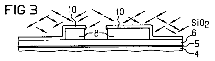
- auxiliary layer 10 is then deposited, as in FIG. 3 is shown.
- a flat angle of incidence i.e. H. in a large angle to the perpendicular to the semiconductor layer planes
- These vaporization directions are in the plane that is perpendicular to the plane of the semiconductor layers and in which the shortest connection between source and drain lies (drawing plane of Figure 3), and are in Figure 3 indicated with the arrows.
- the auxiliary layer is e.g. B. from Silicon dioxide, e.g. B. about 30 nm thick, applied.
- the auxiliary layer is only applied at a maximum thickness that covers the areas intended for source and drain are, but the area intended for the gate inside the Opening of the passivation layer 8 remains free.
- the auxiliary layer can be made from one or more layers of different materials exist and is such that the areas of source and drain during the subsequent process steps remain masked and thus protected.
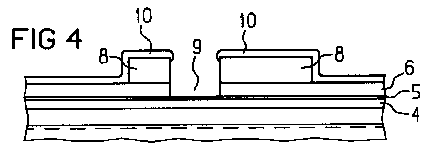
- the ohm contact layer (in this example the cover layer made of InGaAs) is then etched away in the region of the gate to be produced (opening 9).
- This etching step can e.g. B. be carried out wet-chemical, if an etching stop layer 5 made of GaInP is used.
- This etch stop layer 5 should then, for. B. have been grown about 5 nm thick.
- InGaAs can be removed wet-chemically with H 3 PO 4 : H 2 O 2 . If an etch stop layer made of AlAs is used, it is preferably also about 5 nm thick.
- the InGaAs of the ohm contact layer is then removed in a RIE step using Ar: CH 4 : H 2 by dry etching. The structure results, which is shown in cross section in FIG.
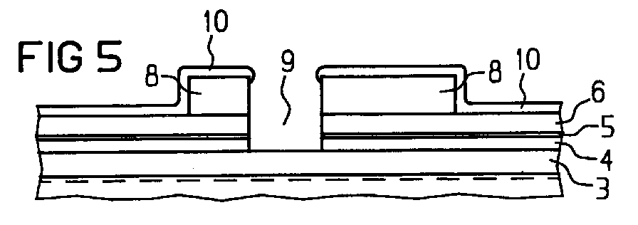
- etch stop layer 5 is then removed.
- An etch stop layer made of GaInP or AlAs is z.
- the etching of the recess to set the threshold voltage of the transistor e.g. HEMT.
- This etching takes place in the intermediate layer 4 down to the channel layer 3 and in this example comprises several substeps.
- the intermediate layer 4 preferably z. B. GaAs is almost completely removed.
- the RF power for excitation of the plasma is switched off.
- the point in time for stopping the etching process is calculated from the etching time for a given etching rate, taking into account the achievable process tolerances up to this point in the etching process. It is then mixed with the gas SF 6 .
- the HF power is switched on and further etched in the Ar: SiCl 4 : SF 6 plasma.
- the etching process reaches the AlGaAs of the channel layer 3, a thin layer (about 2 nm) made of aluminum fluoride (AlF 3 ) forms, depending on the set temperature and the other process parameters, which acts as an etching stop layer, ie significantly reduces the etching rate.
- the excitation of the plasma is then switched off.
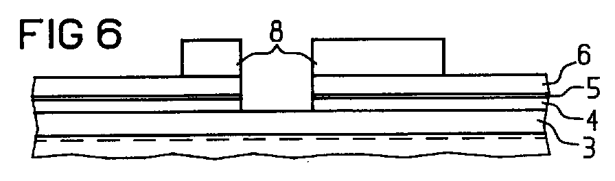
- the etching time with the addition of SF 6 is kept so short because the auxiliary layer 10 made of SiO 2 is simultaneously etched in this etching step.
- spacers are then produced on the flanks of the passivation layer. This is preferably done by depositing a layer over the entire surface and then etching it back anisotropically. It can e.g. B. a layer of Si 3 N 4 is deposited using plasma CVD and then anisotropically etched back in a RIE step using Ar: SF 6 . As a result, the inner spacers 11 and outer spacers 12 are produced on the flanks of the passivation layer 8 (see FIG. 7).
- the end faces of the ohm contact layer made of InGaAs, which face the gate region, are insulated from the gate metal to be subsequently applied by means of these spacers 11, and the gate length of the transistor is defined by the spacers 11.
- a photolithographically defined opening 9 of this passivation layer in the region of the gate to be produced is predefined from 500 nm in the direction from source to drain and the spacers 11 at the base point have an extent of 150 nm, so the gate length is 200 nm.
- the metallization 13 is subsequently etched back in a planarizing manner.
- a planarizing layer 14 e.g. B. from a lacquer, in particular a thermally flowable lacquer (z. B. Accuflo lacquer, protected name of the company Allied Signals), to create a completely planar surface.
- the metallization is again etched back preferably using RIE in an Ar: SF 6 : O 2 plasma until the metallization 13 has been removed to such an extent that a portion 13a (see FIG.
- connection metallization e.g. B. a layer sequence of titanium, platinum and gold can be applied as connection metallization and structured, as shown in Figure 11.
- the dielectric of the passivation layer 8 can also be chosen to be thinner, ie as thin as is minimally required for the necessary passivation.
- the procedure can be varied as follows: According to FIG. 12, a layer sequence consisting of a dielectric layer 80 and one or more metal layers 81, 82 is applied and structured as the passivation layer 8.
- the dielectric layer 80 can also here, for. B. Si 3 N 4 . But it is only z. B. applied about 50 nm thick.
- a metal layer is deposited thereon, which in this exemplary embodiment consists of a thin titanium layer (thickness approximately 10 nm), which serves as an adhesion promoter, and an aluminum layer (thickness approximately 440 nm) applied thereon.
- the structuring of these metal layers takes place, for. B. by means of lifting technology (lift-off).
- the structured metal layer can then be used as a mask for the etching of the dielectric layer 80.
- a dielectric layer 80 made of Si 3 N 4 is z. B. etched away in a RIE step using Ar: SF 6 . In this way, the structure shown in cross section in FIG. 12 is obtained.
- the ohmic contact layer 6 can also preferably be InGaAs that has been doped sufficiently high.
- polyimide lacquer with an integrated adhesion promoter can be used instead of the metal layers 81, 82.
- the polyimide applied to the dielectric layer 80 is baked out at 350 ° C.
- Polyimide with the addition of an adhesion promoter is offered by the paint manufacturers as a finished mixture. By baking, existing solvents are expelled from the lacquer, so that the polyimide is then suitable for further process steps.
- the inner end face (flank) of the metal layers 81, 82 was coated with a thin fluoride layer.
- the aluminum layer 82 given as an example is thus coated with a thin aluminum fluoride layer on the surface.
- This fluoride layer protects the metal against attack by chlorine ions in the subsequent process step in which the intermediate layer 4 made of GaAs is removed by means of RIE in an Ar: SiCl 4 plasma.
- the method steps shown in FIGS. 3 to 9 for the first exemplary embodiment can be carried out accordingly using the modified passivation layer 8 in the second exemplary embodiment.
- the metallization 13 is etched back using RIE in an Ar: SF 6 : O 2 plasma, the aluminum of the metal layer 82 is not etched, the Si 3 N 4 of the dielectric layer 80 is only slightly etched and the tungsten of the metallization 13 is etched with a normal etching rate .
- the structure shown in cross section in FIG. 13 is obtained, in which it can be seen that the metallization again breaks down into a first portion 13a for the gate and a portion 13b separate for the source and drain.
- connection metallization 14 can then be applied and structured again (see FIG. 14), for which purpose a layer sequence of titanium, platinum and gold can also be applied as contact reinforcement.
- the metal of the metal layers 81, 82 (aluminum and titanium in this example) provided for the passivation layer 8 or the polyimide structure can then be removed. This happens in the case of aluminum and titanium z. B. with H 3 PO 4 at room temperature and in the case of polyimide z. B. with isotropic RIE (reactive ion etching) in oxygen plasma. Hot H 3 PO 4 is not used because this would etch the Si 3 N 4 of the dielectric layer 80.
Landscapes
- Junction Field-Effect Transistors (AREA)
- Drying Of Semiconductors (AREA)
Abstract
Description
- Figuren 1 bis 11
- zeigen Zwischenprodukte eines nach dem erfindungsgemäßen Verfahren hergestellten Transistors nach verschiedenen Verfahrensschritten.
- Figuren 12 bis 15
- zeigen die Darstellungen der Figuren 2, 14 und 15 für eine alternative Ausführungsform.
Als Passivierungsschicht 8 wird entsprechend Figur 12 eine Schichtfolge aus einer Dielektrikumschicht 80 und einer oder mehreren Metallschichten 81, 82 aufgebracht und strukturiert. Die Dielektrikumschicht 80 kann auch hier z. B. Si3N4 sein. Es wird hier aber nur z. B. etwa 50 nm dick aufgebracht. Darauf wird eine Metallschicht abgeschieden, die in diesem Ausführungsbeispiel aus einer dünnen Titanschicht (Dicke etwa 10 nm), die als Haftvermittler dient, und einer darauf aufgebrachten Aluminiumschicht (Dicke etwa 440 nm) besteht. Die Strukturierung dieser Metallschichten erfolgt z. B. mittels Abhebetechnik (lift-off). Die strukturierte Metallschicht kann dann als Maske für das Ätzen der Dielektrikumschicht 80 verwendet werden. Eine Dielektrikumschicht 80 aus Si3N4 wird z. B. in einen RIE-Schritt mittels Ar:SF6 weggeätzt. Auf diese Weise erhält man die in Figur 12 im Querschnitt dargestellte Struktur. Die Ohm-Kontaktschicht 6 kann auch hier vorzugsweise InGaAs, das ausreichend hoch dotiert wurde, sein. Statt der Metallschichten 81, 82 kann Polyimidlack mit integriertem Haftvermittler verwendet werden. Das auf die Dielektrikumschicht 80 aufgebrachte Polyimid wird bei 350°C ausgebacken. Polyimid mit Zusatz von Haftvermittler wird von Herstellern des Lackes als fertiges Gemisch angeboten. Durch das Ausbacken werden vorhandene Lösungsmittel aus dem Lack ausgetrieben, so daß das Polyimid anschließend für weitere Prozeßschritte geeignet ist.
Claims (8)
- Verfahren zur Herstellung eines Feldeffekttransistors, bei dem die folgenden Schritte ausgeführt werden:a) Auf ein Substrat (1) aus Halbleitermaterial werden mindestens eine Kanalschicht (2), eine Barriereschicht (3) aus Halbleitermaterial und eine Ohm-Kontaktschicht (6) aus einem für niedrigen ohmschen Widerstand mit einem Metall geeigneten Halbleitermaterial aufgewachsen;b) eine Passivierungsschicht (8) mit einer Öffnung (9) im Bereich eines herzustellenden Gate wird aufgebracht;c) es erfolgt eine Abscheidung einer Hilfsschicht (10) anisotrop und in bezüglich der Halbleiterschichten schräger Einfallsrichtung derart, daß im Bereich dieser Öffnung in der Passivierungsschicht die Oberseite des Halbleitermateriales der Ohm-Kontaktschicht von dem Material dieser Hilfsschicht (10) frei gelassen wird;d) unter Verwendung dieser Hilfsschicht (10) als Maske wird das Halbleitermaterial bis zu der Barriereschicht (3) hinab ausgeätzt;e) die Hilfsschicht wird entfernt;f) durch ganzflächiges isotropes Abscheiden und anschließendes anisotropes Rückätzen einer weiteren Hilfsschicht werden Spacer (11, 12) an den seitlichen Flanken der Passivierungsschicht (8) hergestellt;g) eine hochtemperaturfeste (refractory) Metallisierung (13) wird ganzflächig abgeschieden;h) diese Metallisierung wird soweit planarisierend rückgeätzt, daß separate Kontakte für Source, Gate und Drain übrigbleiben, undi) diese Kontakte werden mit einer Anschlußmetallisierung (14) versehen.
- Verfahren nach Anspruch 1, bei demin Schritt b die Passivierungsschicht (8) als Schichtfolge aus einer Dielektrikumschicht (80) und mindestens einer Metallschicht (81, 82) aufgebracht wird undin Schritt i nach dem Aufbringen der Anschlußmetallisierung (14) die Metallschicht oder Metallschichten der Passivierungsschicht entfernt werden.
- Verfahren nach Anspruch 2, bei demdie Passivierungsschicht (8) als Schichtfolge von Siliziumnitrid (80), Titan (81) und Aluminium (82) hergestellt wird.
- Verfahren nach Anspruch 1, bei demin Schritt b die Passivierungsschicht (8) als Schichtfolge aus einer Dielektrikumschicht (80) und einer Polyimidschicht aufgebracht wird undin Schritt i nach dem Aufbringen der Anschlußmetallisierung (14) die Polyimidschicht entfernt wird.
- Verfahren nach einem der Ansprüche 1 bis 4, bei demin Schritt a die Barriereschicht (3) aus AlGaAs aufgewachsen wird und die Ohm-Kontaktschicht (6) aus InGaAs aufgewachsen wird.
- Verfahren nach einem der Ansprüche 1 bis 5, bei demin Schritt a zwischen der Barriereschicht (3) und der Ohm-Kontaktschicht (6) mindestens eine weitere Schicht aus einem Halbleitermaterial aufgewachsen wird, das selektiv bezüglich der Barriereschicht geätzt werden kann.
- Verfahren nach Anspruch 6, bei demin Schritt a auf eine Schicht (2) aus InGaAs nacheinander eine als Barriereschicht (3) vorgesehene Schicht aus AlGaAs, eine Zwischenschicht (4) aus GaAs, eine als Ätzstoppschicht (5) vorgesehene Schicht aus einem bezüglich InGaAs selektiv ätzbaren Halbleitermaterial und eine als Ohm-Kontaktschicht (6) vorgesehene Schicht aus InGaAs aufgewachsen werden.
- Verfahren nach Anspruch 7, bei demin Schritt b die Passivierungsschicht (8) aus Si3N4 aufgebracht wird,in Schritt c die Hilfsschicht (10) aus SiO2 aufgebracht wird undin Schritt dundi) die Ohm-Kontaktschicht (6) bis zur Ätzstoppschicht (5) hinab entfernt wird,ii) die Ätzstoppschicht (5) entfernt wird,iii) die Zwischenschicht (4) mittels RIE (reactive ion etching) in einem Ar:SiCl4-Plasma fast vollständig entfernt wird,iv) den Gasen des Plasmas in Schritt iii SF6 zugemischt wird,v) der RIE-Prozess in einem Ar:SiCl4:SF6-Plasma fortgesetzt wird, wobei die Temperatur und die restlichen Parameter des Prozesses so eingestellt werden, daß bei Erreichen der Barriereschicht an deren Oberseite eine weitere Ätzstoppschicht aus Aluminiumfluorid gebildet wird,vi) den Gasen des Plasmas in Schritt v SiCl4 entzogen wirdder Schritt e ausgeführt wird, indem der RIE-Prozess in einem Ar:SF6-Plasma fortgesetzt wird.
Applications Claiming Priority (2)
| Application Number | Priority Date | Filing Date | Title |
|---|---|---|---|
| DE19631744 | 1996-08-06 | ||
| DE19631744A DE19631744C1 (de) | 1996-08-06 | 1996-08-06 | Verfahren zur Herstellung eines Feldeffekttransistors |
Publications (3)
| Publication Number | Publication Date |
|---|---|
| EP0823728A2 true EP0823728A2 (de) | 1998-02-11 |
| EP0823728A3 EP0823728A3 (de) | 1998-07-22 |
| EP0823728B1 EP0823728B1 (de) | 2002-04-17 |
Family
ID=7801935
Family Applications (1)
| Application Number | Title | Priority Date | Filing Date |
|---|---|---|---|
| EP97111877A Expired - Lifetime EP0823728B1 (de) | 1996-08-06 | 1997-07-11 | Verfahren zur Herstellung eines Feldeffekttransistors |
Country Status (5)
| Country | Link |
|---|---|
| US (1) | US5960269A (de) |
| EP (1) | EP0823728B1 (de) |
| JP (1) | JPH1079396A (de) |
| CN (1) | CN1080457C (de) |
| DE (2) | DE19631744C1 (de) |
Cited By (1)
| Publication number | Priority date | Publication date | Assignee | Title |
|---|---|---|---|---|
| RU2485621C1 (ru) * | 2011-12-12 | 2013-06-20 | Федеральное государственное унитарное предприятие "Научно-производственное предприятие "Исток" (ФГУП НПП "Исток") | Способ изготовления мощного транзистора свч |
Families Citing this family (6)
| Publication number | Priority date | Publication date | Assignee | Title |
|---|---|---|---|---|
| US6255180B1 (en) * | 1998-05-14 | 2001-07-03 | Cypress Semiconductor Corporation | Semiconductor device with outwardly tapered sidewall spacers and method for forming same |
| DE10304722A1 (de) * | 2002-05-11 | 2004-08-19 | United Monolithic Semiconductors Gmbh | Verfahren zur Herstellung eines Halbleiterbauelements |
| US7535621B2 (en) * | 2006-12-27 | 2009-05-19 | Qualcomm Mems Technologies, Inc. | Aluminum fluoride films for microelectromechanical system applications |
| CN101752241B (zh) * | 2008-12-16 | 2013-04-10 | 上海空间电源研究所 | 大面积GaAs衬底腐蚀工艺 |
| US10685007B2 (en) * | 2016-03-29 | 2020-06-16 | Sap Se | Table content transport and delivery |
| CN109841677A (zh) * | 2019-03-28 | 2019-06-04 | 英诺赛科(珠海)科技有限公司 | 高电子迁移率晶体管及其制造方法 |
Family Cites Families (8)
| Publication number | Priority date | Publication date | Assignee | Title |
|---|---|---|---|---|
| US4377899A (en) * | 1979-11-19 | 1983-03-29 | Sumitomo Electric Industries, Ltd. | Method of manufacturing Schottky field-effect transistors utilizing shadow masking |
| DE3005733A1 (de) * | 1980-02-15 | 1981-08-20 | Siemens AG, 1000 Berlin und 8000 München | Verfahren zur herstellung einer halbleiteranordnung und nach diesem verfahren hergestellte halbleiteranordnung |
| JP2670293B2 (ja) * | 1988-04-15 | 1997-10-29 | 富士通株式会社 | 高電子移動度トランジスタの製造方法 |
| DE3913540A1 (de) * | 1988-09-07 | 1990-03-15 | Licentia Gmbh | Verfahren zur herstellung von steuerelektroden |
| DE4219935C2 (de) * | 1992-06-17 | 1994-06-09 | Siemens Ag | Verfahren zur Herstellung eines Feldeffekttransistors |
| JPH06232168A (ja) * | 1993-02-03 | 1994-08-19 | Sumitomo Electric Ind Ltd | 電界効果トランジスタおよびその製造方法 |
| US5432119A (en) * | 1994-01-31 | 1995-07-11 | Hughes Aircraft Company | High yield electron-beam gate fabrication method for sub-micron gate FETS |
| US5869364A (en) * | 1996-07-22 | 1999-02-09 | The United States Of America As Represented By The Secretary Of The Air Force | Single layer integrated metal process for metal semiconductor field effect transistor (MESFET) |
-
1996
- 1996-08-06 DE DE19631744A patent/DE19631744C1/de not_active Expired - Fee Related
-
1997
- 1997-07-11 EP EP97111877A patent/EP0823728B1/de not_active Expired - Lifetime
- 1997-07-11 DE DE59707017T patent/DE59707017D1/de not_active Expired - Fee Related
- 1997-07-30 JP JP9219249A patent/JPH1079396A/ja active Pending
- 1997-08-06 US US08/906,780 patent/US5960269A/en not_active Expired - Fee Related
- 1997-08-06 CN CN97115399A patent/CN1080457C/zh not_active Expired - Fee Related
Cited By (1)
| Publication number | Priority date | Publication date | Assignee | Title |
|---|---|---|---|---|
| RU2485621C1 (ru) * | 2011-12-12 | 2013-06-20 | Федеральное государственное унитарное предприятие "Научно-производственное предприятие "Исток" (ФГУП НПП "Исток") | Способ изготовления мощного транзистора свч |
Also Published As
| Publication number | Publication date |
|---|---|
| CN1175086A (zh) | 1998-03-04 |
| EP0823728B1 (de) | 2002-04-17 |
| DE59707017D1 (de) | 2002-05-23 |
| EP0823728A3 (de) | 1998-07-22 |
| CN1080457C (zh) | 2002-03-06 |
| JPH1079396A (ja) | 1998-03-24 |
| US5960269A (en) | 1999-09-28 |
| DE19631744C1 (de) | 1998-03-12 |
Similar Documents
| Publication | Publication Date | Title |
|---|---|---|
| DE102008052595B4 (de) | Verfahren zur Herstellung eines Halbleiterbauelements als High-Electron-Mobility-Transistorhalbleiterbauelement (HEMT) mit feldabschwächender Platte und Halbleiterbauelement | |
| DE68918773T2 (de) | Verfahren zur Herstellung einer Halbleitervorrichtung mit mindestens einer kleine Kontaktlöcher enthaltenden Leiterbahn. | |
| EP1508164B1 (de) | Verfahren zur herstellung eines halbleiterbauelementes und danach hergestelltes halbleiterbaulelement | |
| DE112017007305B4 (de) | Verfahren zur Herstellung einer Halbleitervorrichtung und Halbleitervorrichtung | |
| DE4138842C2 (de) | Gateelektrode und Verfahren zu deren Herstellung | |
| DE3245276A1 (de) | Verfahren zum ausbilden von submikrometer-merkmalen in halbleiterbauelementen | |
| DE69835204T2 (de) | ENTWURF UND HERSTELLUNG VON ELEKTRONISCHEN ANORDNUNGEN MIT InAlAsSb/AlSb BARRIERE | |
| EP0308939B1 (de) | Verfahren zur Herstellung eines MESFET mit selbstjustiertem Gate | |
| AT506666A2 (de) | Aufbau und verfahren zum ausbilden eines planaren schottky-kontakts | |
| DE69434162T2 (de) | Verfahren zur Herstellung einer Gate-Elektrode aus schwerschmelzendem Metall | |
| DE102008060704A1 (de) | Zusammengesetzter Passivierungsprozess für Nitrid-Feldeffekttransistoren | |
| EP0182088B1 (de) | Schottky-Kontakt auf einer Halbleiteroberfläche und Verfahren zu dessen Herstellung | |
| DE3885255T2 (de) | Verfahren zum Herstellen eines Galliumarsenid-Feldeffekt-Transistors. | |
| DE3933965C2 (de) | ||
| DE69930135T2 (de) | Pseudomorphe transistoren mit hoher elektronenbeweglichkeit | |
| WO2018104136A1 (de) | Verfahren zur herstellung eines transistors | |
| DE69531228T2 (de) | Verfahren zur Herstellung eines MESFETS mit einer T-förmigen Gate-Elektrode und dadurch hergestelltes Bauelement | |
| EP0823728B1 (de) | Verfahren zur Herstellung eines Feldeffekttransistors | |
| EP1354342B1 (de) | Verfahren zur herstellung eines halbleiter-bauelements mit einer t-förmigen kontaktelektrode | |
| EP0416141A1 (de) | Verfahren zur Herstellung eines FET mit asymmetrisch angeordnetem Gate-Bereich | |
| DE69132301T2 (de) | Verfahren zur Herstellung eines Verbindungshalbleiterbauelements und damit hergestelltes Verbindungshalbleiterbauelement | |
| DE3538855A1 (de) | Verfahren zur herstellung einer halbleitervorrichtung | |
| EP2230684B1 (de) | Herstellungsverfahren für integrierte Schaltungsanordnung mit niederohmigen Kontakten | |
| DE102016122399A1 (de) | Gate-Struktur und Verfahren zu dessen Herstellung | |
| DE3706274A1 (de) | Halbleiterelement und verfahren zu dessen herstellung |
Legal Events
| Date | Code | Title | Description |
|---|---|---|---|
| PUAI | Public reference made under article 153(3) epc to a published international application that has entered the european phase |
Free format text: ORIGINAL CODE: 0009012 |
|
| AK | Designated contracting states |
Kind code of ref document: A2 Designated state(s): DE FR GB |
|
| AX | Request for extension of the european patent |
Free format text: AL;LT;LV;RO;SI |
|
| PUAL | Search report despatched |
Free format text: ORIGINAL CODE: 0009013 |
|
| AK | Designated contracting states |
Kind code of ref document: A3 Designated state(s): AT BE CH DE DK ES FI FR GB GR IE IT LI LU MC NL PT SE |
|
| AX | Request for extension of the european patent |
Free format text: AL;LT;LV;RO;SI |
|
| 17P | Request for examination filed |
Effective date: 19980805 |
|
| AKX | Designation fees paid |
Free format text: DE FR GB |
|
| RBV | Designated contracting states (corrected) |
Designated state(s): DE FR GB |
|
| GRAG | Despatch of communication of intention to grant |
Free format text: ORIGINAL CODE: EPIDOS AGRA |
|
| 17Q | First examination report despatched |
Effective date: 20010904 |
|
| GRAG | Despatch of communication of intention to grant |
Free format text: ORIGINAL CODE: EPIDOS AGRA |
|
| GRAH | Despatch of communication of intention to grant a patent |
Free format text: ORIGINAL CODE: EPIDOS IGRA |
|
| RAP1 | Party data changed (applicant data changed or rights of an application transferred) |
Owner name: INFINEON TECHNOLOGIES AG |
|
| REG | Reference to a national code |
Ref country code: GB Ref legal event code: IF02 |
|
| GRAH | Despatch of communication of intention to grant a patent |
Free format text: ORIGINAL CODE: EPIDOS IGRA |
|
| GRAA | (expected) grant |
Free format text: ORIGINAL CODE: 0009210 |
|
| AK | Designated contracting states |
Kind code of ref document: B1 Designated state(s): DE FR GB |
|
| REF | Corresponds to: |
Ref document number: 59707017 Country of ref document: DE Date of ref document: 20020523 |
|
| PGFP | Annual fee paid to national office [announced via postgrant information from national office to epo] |
Ref country code: GB Payment date: 20020711 Year of fee payment: 6 |
|
| PGFP | Annual fee paid to national office [announced via postgrant information from national office to epo] |
Ref country code: FR Payment date: 20020726 Year of fee payment: 6 |
|
| GBT | Gb: translation of ep patent filed (gb section 77(6)(a)/1977) |
Effective date: 20020709 |
|
| PGFP | Annual fee paid to national office [announced via postgrant information from national office to epo] |
Ref country code: DE Payment date: 20020916 Year of fee payment: 6 |
|
| ET | Fr: translation filed | ||
| PLBE | No opposition filed within time limit |
Free format text: ORIGINAL CODE: 0009261 |
|
| STAA | Information on the status of an ep patent application or granted ep patent |
Free format text: STATUS: NO OPPOSITION FILED WITHIN TIME LIMIT |
|
| 26N | No opposition filed |
Effective date: 20030120 |
|
| PG25 | Lapsed in a contracting state [announced via postgrant information from national office to epo] |
Ref country code: GB Free format text: LAPSE BECAUSE OF NON-PAYMENT OF DUE FEES Effective date: 20030711 |
|
| PG25 | Lapsed in a contracting state [announced via postgrant information from national office to epo] |
Ref country code: DE Free format text: LAPSE BECAUSE OF NON-PAYMENT OF DUE FEES Effective date: 20040203 |
|
| GBPC | Gb: european patent ceased through non-payment of renewal fee |
Effective date: 20030711 |
|
| PG25 | Lapsed in a contracting state [announced via postgrant information from national office to epo] |
Ref country code: FR Free format text: LAPSE BECAUSE OF NON-PAYMENT OF DUE FEES Effective date: 20040331 |
|
| REG | Reference to a national code |
Ref country code: FR Ref legal event code: ST |