EP0823732B1 - Filmträger und diesen verwendende Halbleiteranordnung - Google Patents
Filmträger und diesen verwendende Halbleiteranordnung Download PDFInfo
- Publication number
- EP0823732B1 EP0823732B1 EP96112701A EP96112701A EP0823732B1 EP 0823732 B1 EP0823732 B1 EP 0823732B1 EP 96112701 A EP96112701 A EP 96112701A EP 96112701 A EP96112701 A EP 96112701A EP 0823732 B1 EP0823732 B1 EP 0823732B1
- Authority
- EP
- European Patent Office
- Prior art keywords
- film carrier
- conductive
- conductive circuit
- insulating substrate
- opening
- Prior art date
- Legal status (The legal status is an assumption and is not a legal conclusion. Google has not performed a legal analysis and makes no representation as to the accuracy of the status listed.)
- Expired - Lifetime
Links
Images


Classifications
-
- H—ELECTRICITY
- H05—ELECTRIC TECHNIQUES NOT OTHERWISE PROVIDED FOR
- H05K—PRINTED CIRCUITS; CASINGS OR CONSTRUCTIONAL DETAILS OF ELECTRIC APPARATUS; MANUFACTURE OF ASSEMBLAGES OF ELECTRICAL COMPONENTS
- H05K3/00—Apparatus or processes for manufacturing printed circuits
- H05K3/40—Forming printed elements for providing electric connections to or between printed circuits
- H05K3/4007—Surface contacts, e.g. bumps
-
- H—ELECTRICITY
- H10—SEMICONDUCTOR DEVICES; ELECTRIC SOLID-STATE DEVICES NOT OTHERWISE PROVIDED FOR
- H10W—GENERIC PACKAGES, INTERCONNECTIONS, CONNECTORS OR OTHER CONSTRUCTIONAL DETAILS OF DEVICES COVERED BY CLASS H10
- H10W70/00—Package substrates; Interposers; Redistribution layers [RDL]
- H10W70/60—Insulating or insulated package substrates; Interposers; Redistribution layers
- H10W70/67—Insulating or insulated package substrates; Interposers; Redistribution layers characterised by their insulating layers or insulating parts
- H10W70/688—Flexible insulating substrates
-
- H—ELECTRICITY
- H10—SEMICONDUCTOR DEVICES; ELECTRIC SOLID-STATE DEVICES NOT OTHERWISE PROVIDED FOR
- H10W—GENERIC PACKAGES, INTERCONNECTIONS, CONNECTORS OR OTHER CONSTRUCTIONAL DETAILS OF DEVICES COVERED BY CLASS H10
- H10W90/00—Package configurations
- H10W90/701—Package configurations characterised by the relative positions of pads or connectors relative to package parts
-
- H—ELECTRICITY
- H05—ELECTRIC TECHNIQUES NOT OTHERWISE PROVIDED FOR
- H05K—PRINTED CIRCUITS; CASINGS OR CONSTRUCTIONAL DETAILS OF ELECTRIC APPARATUS; MANUFACTURE OF ASSEMBLAGES OF ELECTRICAL COMPONENTS
- H05K2201/00—Indexing scheme relating to printed circuits covered by H05K1/00
- H05K2201/03—Conductive materials
- H05K2201/0332—Structure of the conductor
- H05K2201/0335—Layered conductors or foils
- H05K2201/0347—Overplating, e.g. for reinforcing conductors or bumps; Plating over filled vias
-
- H—ELECTRICITY
- H05—ELECTRIC TECHNIQUES NOT OTHERWISE PROVIDED FOR
- H05K—PRINTED CIRCUITS; CASINGS OR CONSTRUCTIONAL DETAILS OF ELECTRIC APPARATUS; MANUFACTURE OF ASSEMBLAGES OF ELECTRICAL COMPONENTS
- H05K2201/00—Indexing scheme relating to printed circuits covered by H05K1/00
- H05K2201/03—Conductive materials
- H05K2201/0332—Structure of the conductor
- H05K2201/0335—Layered conductors or foils
- H05K2201/0355—Metal foils
-
- H—ELECTRICITY
- H05—ELECTRIC TECHNIQUES NOT OTHERWISE PROVIDED FOR
- H05K—PRINTED CIRCUITS; CASINGS OR CONSTRUCTIONAL DETAILS OF ELECTRIC APPARATUS; MANUFACTURE OF ASSEMBLAGES OF ELECTRICAL COMPONENTS
- H05K2201/00—Indexing scheme relating to printed circuits covered by H05K1/00
- H05K2201/03—Conductive materials
- H05K2201/0332—Structure of the conductor
- H05K2201/0364—Conductor shape
- H05K2201/0367—Metallic bump or raised conductor not used as solder bump
-
- H—ELECTRICITY
- H05—ELECTRIC TECHNIQUES NOT OTHERWISE PROVIDED FOR
- H05K—PRINTED CIRCUITS; CASINGS OR CONSTRUCTIONAL DETAILS OF ELECTRIC APPARATUS; MANUFACTURE OF ASSEMBLAGES OF ELECTRICAL COMPONENTS
- H05K2201/00—Indexing scheme relating to printed circuits covered by H05K1/00
- H05K2201/03—Conductive materials
- H05K2201/0332—Structure of the conductor
- H05K2201/0388—Other aspects of conductors
- H05K2201/0394—Conductor crossing over a hole in the substrate or a gap between two separate substrate parts
-
- H—ELECTRICITY
- H05—ELECTRIC TECHNIQUES NOT OTHERWISE PROVIDED FOR
- H05K—PRINTED CIRCUITS; CASINGS OR CONSTRUCTIONAL DETAILS OF ELECTRIC APPARATUS; MANUFACTURE OF ASSEMBLAGES OF ELECTRICAL COMPONENTS
- H05K2201/00—Indexing scheme relating to printed circuits covered by H05K1/00
- H05K2201/09—Shape and layout
- H05K2201/09209—Shape and layout details of conductors
- H05K2201/09372—Pads and lands
- H05K2201/09481—Via in pad; Pad over filled via
-
- H—ELECTRICITY
- H05—ELECTRIC TECHNIQUES NOT OTHERWISE PROVIDED FOR
- H05K—PRINTED CIRCUITS; CASINGS OR CONSTRUCTIONAL DETAILS OF ELECTRIC APPARATUS; MANUFACTURE OF ASSEMBLAGES OF ELECTRICAL COMPONENTS
- H05K2201/00—Indexing scheme relating to printed circuits covered by H05K1/00
- H05K2201/09—Shape and layout
- H05K2201/09209—Shape and layout details of conductors
- H05K2201/095—Conductive through-holes or vias
- H05K2201/09563—Metal filled via
-
- H—ELECTRICITY
- H05—ELECTRIC TECHNIQUES NOT OTHERWISE PROVIDED FOR
- H05K—PRINTED CIRCUITS; CASINGS OR CONSTRUCTIONAL DETAILS OF ELECTRIC APPARATUS; MANUFACTURE OF ASSEMBLAGES OF ELECTRICAL COMPONENTS
- H05K2201/00—Indexing scheme relating to printed circuits covered by H05K1/00
- H05K2201/09—Shape and layout
- H05K2201/09209—Shape and layout details of conductors
- H05K2201/09654—Shape and layout details of conductors covering at least two types of conductors provided for in H05K2201/09218 - H05K2201/095
- H05K2201/09745—Recess in conductor, e.g. in pad or in metallic substrate
-
- H—ELECTRICITY
- H05—ELECTRIC TECHNIQUES NOT OTHERWISE PROVIDED FOR
- H05K—PRINTED CIRCUITS; CASINGS OR CONSTRUCTIONAL DETAILS OF ELECTRIC APPARATUS; MANUFACTURE OF ASSEMBLAGES OF ELECTRICAL COMPONENTS
- H05K2203/00—Indexing scheme relating to apparatus or processes for manufacturing printed circuits covered by H05K3/00
- H05K2203/03—Metal processing
- H05K2203/0369—Etching selective parts of a metal substrate through part of its thickness, e.g. using etch resist
-
- H—ELECTRICITY
- H05—ELECTRIC TECHNIQUES NOT OTHERWISE PROVIDED FOR
- H05K—PRINTED CIRCUITS; CASINGS OR CONSTRUCTIONAL DETAILS OF ELECTRIC APPARATUS; MANUFACTURE OF ASSEMBLAGES OF ELECTRICAL COMPONENTS
- H05K2203/00—Indexing scheme relating to apparatus or processes for manufacturing printed circuits covered by H05K3/00
- H05K2203/09—Treatments involving charged particles
- H05K2203/095—Plasma, e.g. for treating a substrate to improve adhesion with a conductor or for cleaning holes
-
- H—ELECTRICITY
- H05—ELECTRIC TECHNIQUES NOT OTHERWISE PROVIDED FOR
- H05K—PRINTED CIRCUITS; CASINGS OR CONSTRUCTIONAL DETAILS OF ELECTRIC APPARATUS; MANUFACTURE OF ASSEMBLAGES OF ELECTRICAL COMPONENTS
- H05K2203/00—Indexing scheme relating to apparatus or processes for manufacturing printed circuits covered by H05K3/00
- H05K2203/15—Position of the PCB during processing
- H05K2203/1572—Processing both sides of a PCB by the same process; Providing a similar arrangement of components on both sides; Making interlayer connections from two sides
-
- H—ELECTRICITY
- H05—ELECTRIC TECHNIQUES NOT OTHERWISE PROVIDED FOR
- H05K—PRINTED CIRCUITS; CASINGS OR CONSTRUCTIONAL DETAILS OF ELECTRIC APPARATUS; MANUFACTURE OF ASSEMBLAGES OF ELECTRICAL COMPONENTS
- H05K3/00—Apparatus or processes for manufacturing printed circuits
- H05K3/0011—Working of insulating substrates or insulating layers
- H05K3/0017—Etching of the substrate by chemical or physical means
- H05K3/0026—Etching of the substrate by chemical or physical means by laser ablation
- H05K3/0032—Etching of the substrate by chemical or physical means by laser ablation of organic insulating material
- H05K3/0035—Etching of the substrate by chemical or physical means by laser ablation of organic insulating material of blind holes, i.e. having a metal layer at the bottom
-
- H—ELECTRICITY
- H05—ELECTRIC TECHNIQUES NOT OTHERWISE PROVIDED FOR
- H05K—PRINTED CIRCUITS; CASINGS OR CONSTRUCTIONAL DETAILS OF ELECTRIC APPARATUS; MANUFACTURE OF ASSEMBLAGES OF ELECTRICAL COMPONENTS
- H05K3/00—Apparatus or processes for manufacturing printed circuits
- H05K3/0011—Working of insulating substrates or insulating layers
- H05K3/0055—After-treatment, e.g. cleaning or desmearing of holes
-
- H—ELECTRICITY
- H05—ELECTRIC TECHNIQUES NOT OTHERWISE PROVIDED FOR
- H05K—PRINTED CIRCUITS; CASINGS OR CONSTRUCTIONAL DETAILS OF ELECTRIC APPARATUS; MANUFACTURE OF ASSEMBLAGES OF ELECTRICAL COMPONENTS
- H05K3/00—Apparatus or processes for manufacturing printed circuits
- H05K3/40—Forming printed elements for providing electric connections to or between printed circuits
- H05K3/42—Plated through-holes or plated via connections
- H05K3/423—Plated through-holes or plated via connections characterised by electroplating method
-
- H—ELECTRICITY
- H10—SEMICONDUCTOR DEVICES; ELECTRIC SOLID-STATE DEVICES NOT OTHERWISE PROVIDED FOR
- H10W—GENERIC PACKAGES, INTERCONNECTIONS, CONNECTORS OR OTHER CONSTRUCTIONAL DETAILS OF DEVICES COVERED BY CLASS H10
- H10W70/00—Package substrates; Interposers; Redistribution layers [RDL]
- H10W70/60—Insulating or insulated package substrates; Interposers; Redistribution layers
- H10W70/62—Insulating or insulated package substrates; Interposers; Redistribution layers characterised by their interconnections
- H10W70/65—Shapes or dispositions of interconnections
- H10W70/654—Top-view layouts
- H10W70/655—Fan-out layouts
-
- H—ELECTRICITY
- H10—SEMICONDUCTOR DEVICES; ELECTRIC SOLID-STATE DEVICES NOT OTHERWISE PROVIDED FOR
- H10W—GENERIC PACKAGES, INTERCONNECTIONS, CONNECTORS OR OTHER CONSTRUCTIONAL DETAILS OF DEVICES COVERED BY CLASS H10
- H10W70/00—Package substrates; Interposers; Redistribution layers [RDL]
- H10W70/60—Insulating or insulated package substrates; Interposers; Redistribution layers
- H10W70/62—Insulating or insulated package substrates; Interposers; Redistribution layers characterised by their interconnections
- H10W70/65—Shapes or dispositions of interconnections
- H10W70/654—Top-view layouts
- H10W70/656—Fan-in layouts
-
- H—ELECTRICITY
- H10—SEMICONDUCTOR DEVICES; ELECTRIC SOLID-STATE DEVICES NOT OTHERWISE PROVIDED FOR
- H10W—GENERIC PACKAGES, INTERCONNECTIONS, CONNECTORS OR OTHER CONSTRUCTIONAL DETAILS OF DEVICES COVERED BY CLASS H10
- H10W90/00—Package configurations
- H10W90/701—Package configurations characterised by the relative positions of pads or connectors relative to package parts
- H10W90/721—Package configurations characterised by the relative positions of pads or connectors relative to package parts of bump connectors
- H10W90/724—Package configurations characterised by the relative positions of pads or connectors relative to package parts of bump connectors between a chip and a stacked insulating package substrate, interposer or RDL
Definitions
- the present invention relates to a film carrier to be used for mounting a semiconductor element, and a semiconductor device comprising a semiconductor element mounted on said film carrier.
- a semiconductor element has been conventionally mounted by a film carrier method.
- semiconductor chips are connected via bumps to a film carrier tape which functions as a member for carrying a semiconductor element or for packaging same.
- a bump is a conductive protruding connection which is formed on an electrode surface of a semiconductor element as an inner bonding means to connect a lead on a film carrier and the electrode of the semiconductor element.
- an adhesive metal layer of, for example, titanium and chromium, and a barrier metal layer of, for example, copper, platinum and palladium for the prevention of diffusion of bump metals need to be formed on the electrode surface by sputter-etching, evaporation deposition and the like, and a bump of gold, etc. is formed thereon.
- the fabrication becomes extremely complicated.
- the semiconductor element and the electrode surface may be contaminated or damaged while forming bumps on the electrode surface.
- anisotropic conductive film examples include those containing conductive particles, such as carbon black, graphite, nickel, copper and silver, oriented in an insulating film in the direction of the film thickness and dispersed therein.
- anisotropic conductive film is associated with difficulties in that insufficient orientation of the conductive particles leads to an uncertain electrical connection between the lead on the film carrier and the electrode of the semiconductor element, which in turn causes poor connection reliability.
- a film carrier having a conductive circuit and a lead on the surface of an insulating film may be used.
- this method is again associated with potential difficulty in coping with miniaturization of semiconductor elements, since the area of outer lead bonding routinely becomes greater than the area of inner lead bonding, thereby making the final mounting area greater than the area of the semiconductor element.
- a semiconductor element mounted on a film carrier is often protected by molding and sealing same with an insulating resin.
- an insulating sealant resin directly contacts said conductive circuit.
- the metal constituting the conductive circuit and the insulating resin adhere poorly to each other, allowing water in the air and other substances to intrude into the interface of the two to possibly degrade the reliability of the semiconductor device obtained.
- a film carrier which can sufficiently cope with a fine-pitched or highly dense wiring of a semiconductor element, can provide positive connections both in inner lead bonding and outer lead bonding, and which can make the mounting area as small as possible.
- the structure of this film carrier is that wherein a conductive circuit is not formed on an insulating film but completely embedded in the insulating film, an opening is formed in the insulating film to expose the surface of the embedded conductive circuit, and a conductor is filled in said opening to form a conductive path to allow electrical connection between the conductive circuit and the electrode of a semiconductor element or the landing part of an external substrate via the surface of this conductive path.
- This structure is again associated with a problem in that the conductive path may come off from the insulating film when a defective semiconductor element is replaced after connection with the external substrate using solder, etc., due to a low adhesion strength between said conductive path and conductive circuit.
- Another object of the present invention is to provide a semiconductor device having the characteristics of the film carrier of the present invention after connection of the film carrier to a semiconductor element.
- the film carrier of the present invention is characterized in that a conductive circuit is formed on one side or inside of an insulating substrate, and
- the semiconductor device of the present invention comprises an electrode of the semiconductor element connected to the contact part of the film carrier of the present invention.
- semiconductor element encompasses an assembly of semiconductor elements as a matrix on a silicon wafer and individual silicon chips after dicing same, a circuit substrate for mounting on a semiconductor device, a circuit substrate for LCD, and a fine-pitched circuit substrate such as hybrid IC, and a "conductive circuit” denotes a wide concept inclusive of not only wiring patterns, but also electrode, lead and the like.
- Fig. 1 is a schematic showing of one embodiment of the film carrier of the present invention.
- Fig. 2 is a schematic showing of another embodiment of the film carrier of the present invention wherein openings are formed on both sides of an insulating substrate.
- Fig. 3 (A) is a schematic cross section of one embodiment of the semiconductor device of the present invention.
- Fig. 3 (B) is a schematic cross section of another embodiment of the semiconductor device of the present invention.
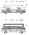
- Fig. 4 is a schematic cross section of one embodiment of the method of the present invention for producing a semiconductor element.
- Fig. 1 is a schematic showing of one embodiment of the film carrier of the present invention, which is a cross section along the line of the lengthwise axis of the opening.
- This embodiment shows a film carrier of the present invention having an opening only on one side of the insulating substrate.
- the structure of the film carrier of the present invention is such that a conductive circuit 2 is formed inside an insulating substrate 1, an opening 3 is formed at a desired position on one side of said insulating substrate 1, the conductive circuit is exposed at the bottom of the opening 3, and a conductive material is filled in said opening to form a conductive path 4.
- the upper end of the conductive path 4 functions as a contact part 5 to make an electric connection with external contact objects.
- the conductive material filled in the opening protrudes from the surface of the insulating substrate to form a bump to be a contact part 5.
- the opening 3 consists of a through-hole 3a extending from a surface 1a of the insulating substrate 1 to a surface 2a of the conductive circuit 2, and a concave formed on the face of the conductive circuit about the opening at the lower end of said through-hole in a diameter equally extended all around said opening, wherein the through-hole and the concave form a mushroom shape.
- Fig. 1 only the conductive circuit 2 is hatched.
- Y is preferably always not more than 1/2 of Z.
- the concave may disadvantageously penetrate the conductive circuit.
- X is preferably always not more than 1/2 of W.
- X is greater than 1/2 of W, the adhesion between the insulating substrate and conductive circuit becomes problematically low.
- X/Y is preferably not less than 1/3 and not more than 1.
- X/Y is less than 1/3, the shortness of X makes catch on the insulating substrate smaller. As a result, a tensile strength becomes low, so that the conductive path tends to come off easily from the opening.
- X/Y is greater than 1, X is long but Y becomes short, so that a shear strength becomes small.
- the material of the insulating substrate is not subject to any particular limitation as long as it can stably support the internal conductive circuit, conductive path from the inside to the surface, and in some cases, bumps on the surface, and is substantially electrically insulating.
- Specific examples include various thermosetting resins and thermoplastic resins such as polyester resin, epoxy resin, urethane resin, polystyrene resin, polyethylene resin, polyamide resin, polyimide resin, acrylonitrile-butadiene-styrene copolymer resin (ABS resin), polycarbonate resin, silicone resin and fluororesin, with preference given to polyimide resin in view of the superior heat resistance, dimensional stability on heating and mechanical strength.
- the thickness of the insulating layer is not particularly limited, it is about 2-500 ⁇ m, preferably about 5-150 ⁇ m, to achieve sufficient mechanical strength and flexibility.
- the conductive circuit may be formed inside the insulating substrate or on the substrate on the side without the opening.
- the material of the conductive circuit is subject to no particular limitation as long as it has conductivity, and is exemplified by various metals.
- Preferred is copper since it has smaller resistance and can reduce the width of wiring area to realize finer pitches and send signals at higher speeds.
- the thickness of the conductive circuit is not particularly limited, it is generally about 1-200 ⁇ m, preferably about 5-80 ⁇ m.
- the shape and size of the opening can be determined in consideration of the width of the conductive circuit contained inside, according to the structure wherein, for example, a conductive material is filled in the opening and the opening of the insulating substrate is used as a contact part, or wherein a bump is formed and the opening is used as a conductive path between the bump and the conductive circuit.
- the shape of the through-hole is mainly columnar or a circular cone.
- the size of the opening on the surface of the insulating substrate is preferably about 5 ⁇ m - 200 ⁇ m, preferably 8 ⁇ m - 100 ⁇ m.
- the shape of the concave to be formed as a part of the opening in the conductive circuit may be any as long as it has greater diameter than the diameter of the lower end of the through-hole, and may be, for example, a semi-sphere or trapezoid.
- the opening may be formed by a known method generally used for making an opening in a substrate. Since the through-hole and the concave are formed from different materials, they may be formed by different methods.
- the through-hole may be formed by, for example, mechanical processing such as punching, photolithographic processing, plasma processing, chemical etching processing and laser processing, with preference given to laser processing which enables elaborate processing required for fine-pitched products.
- mechanical processing such as punching, photolithographic processing, plasma processing, chemical etching processing and laser processing
- laser processing which enables elaborate processing required for fine-pitched products.
- the use of an ultraviolet laser having an oscillation wavelength in the ultraviolet range is preferable.
- the concave in the conductive circuit can be formed by, for example, dry etching using CO 2 laser or wet etching such as chemical etching and electrolytic etching.
- dry etching using CO 2 laser or wet etching such as chemical etching and electrolytic etching.
- chemical etching is preferable which affords uniform etching and is superior in mass production.
- the depth and outer diameter of the concave, in particular, X and Y mentioned above are adjusted by varying liquid components, temperature, time, the amount and manner of liquids applied and the like.
- the opening may be formed on both sides of the insulating substrate.
- a conductive circuit may be made between the concaves of a desired combination of, from among the openings on both sides of substrate, 31 and 34, or 32 and 33. This construction provides a superior film carrier which conducts in the direction penetrating the plane of the insulating substrate.
- the conductive material to be filled in the opening is subject to no particular limitation as long as it has conductivity, and may be known metallic materials, such as gold, silver, copper, platinum, zinc, tin, nickel, cobalt, indium, rhodium, chromium, tungsten and ruthenium, and various alloys containing same as components (e.g., solder, nickel-tin and gold-cobalt).
- metallic materials such as gold, silver, copper, platinum, zinc, tin, nickel, cobalt, indium, rhodium, chromium, tungsten and ruthenium, and various alloys containing same as components (e.g., solder, nickel-tin and gold-cobalt).
- the material to be used for filling in the opening and the material of the bump may be the same or different and are determined according to the object.
- the conductive path 4 including the concave 3c to be connected to the conductive circuit 2 is made from an economical metal having lower resistance, such as copper, and the surface layer of bump 5 to be in contact with the electrode of a semiconductor element is made from a material reliable in connection performance, such as gold.
- the surface layer of the bump is formed using a material which becomes easily wet to the solder, such as gold, platinum and tin, and a material which hardly becomes wet to the solder, such as nickel, tungsten and tantalum, is preferably used in between the surface layer of the bump and the conductive path.
- the method for filling a conductive material in the opening includes, for example, plating method such as electrolytic plating and electroless plating, CVD, chemical filling which comprises immersing the opening into a melt metal bath to allow precipitation of a conductive substance, and physical filling method comprising injecting a conductive substance into the opening with pressure, with preference given to an electrolytic plating using a conductive circuit as an electrode for the easiness of processing. Therefore, filling of a conductive substance in the present invention denotes a wide concept inclusive of mechanical filling of conductive substances and the above-mentioned chemical precipitation as well.
- the height of the bump is not particularly limited, it is suitably about 3-30 ⁇ m to deal with small semiconductor elements.
- the shape of the bump may be any as long as it can make electrical contact with the contact target.
- it may be like a mushroom (umbrella) as shown in Fig. 1, semi-sphere, prism, column, sphere or cone (e.g., circular cone and pyramid).
- the shape of the bump on the plane of the insulating substrate may be, for example, triangle, square, rectangle, trapezoid, parallelogram or other polygon.
- bumps contributes to easy positioning of connections and ensured connections with electrodes of semiconductor elements or landing parts of external substrates.
- a design not to form the end of a conductive path into a bump but to level same with the surface of the insulating substrate, or form same into concaves may be adapted according to the shape of the contacting mate, and an optional design may be employed depending on the layout of the semiconductor element and external substrate to be connected to the film carrier, the shape of the circuit and the like.
- One embodiment of the semiconductor device is shown in the following, which is obtained by connecting a semiconductor element to the film carrier of the present invention.
- Fig. 3(A) and Fig. 3(B) are schematic cross sections of the embodiments of the semiconductor device of the present invention. In these Figures, hatching distinguishes regions.
- a film carrier A has any necessary number of openings on both sides and a conductive path having a bump at the top surface, like the embodiment shown in Fig. 2, wherein a semiconductor element B is connected to one side of the film carrier, and an insulating resin C molds the semiconductor element and almost the entire surface of one side of the film carrier to which the semiconductor element has been connected.
- conductive circuits 21 and 22 are different systems of insulated circuits, and are embedded in the flexible insulating substrate 1.
- Bumps 51a and 51b, and 52a and 52b formed on both sides of the insulating substrate 1 are each conducted by conductive circuits 21 and 22, respectively, and the bumps 51a and 52a formed on one side are electrically connected to electrodes B1 and B2, respectively, which have been formed on the semiconductor element B.
- the bumps 51a, 51b, 52a and 52b are not formed right behind of respective mating bumps but located in slantwise positions relative to the lengthwise direction of each conductive circuit. The difference between the embodiments of Fig. 3(A) and Fig.
- 3(B) lies in the locational relationship between the bumps formed on both sides of the substrate 22 in the film carrier A to be used.
- the bumps 51b and 52b exposed on the surface of the semiconductor device are located in slantwise positions relative to the bumps 51a and 52a inside the semiconductor device, toward the outer periphery of substrate in Fig. 3(A) and otherwise in Fig. 3(B).
- Fig. 3(A) the bumps 51a and 52a inside the semiconductor device
- the bumps 51b and 52b exposed on the surface of the semiconductor device are located toward the center of the substrate from the bumps 51a and 52a, respectively, thereby advantageously obviating an increase in the area of the film carrier A and decreasing the area occupied by this semiconductor device to the area same as that of the semiconductor element B on the film carrier.
- This embodiment is particularly preferable because, when a number of semiconductor devices of Fig. 3(B) are mounted at high density to the extent that they are located just next to each other on a mating circuit substrate, for example, a conductor to be formed on the mating circuit substrate, which corresponds to one semiconductor device, does not come too close to the next conductor corresponding to the next semiconductor device, but can desirably secure a sufficient insulating distance.
- the electrodes B1, B2 of the semiconductor element B and the landing part are conducted in the anisotropic direction (thickness direction of insulating layer).
- a known insulating resin such as epoxy resin and silicone resin can be used for molding and sealing the semiconductor element.
- the insulating resin for molding does not come into contact with conductive circuit, but comes into contact with insulating substrate alone to form an interface.
- the film carrier shows superior adhesion to the insulating substrate, thus obviating intrusion of water into the interface, and has greatly improved reliability as a semiconductor device.
- FIG. 4 schematically shows one embodiment thereof.
- reference numerals for the same parts appearing in the preceding Figures have been omitted.
- the processing into each shape is as explained in Fig. 1 above.
- the method for sealing may be a known method such as potting and casting, besides the method used in Fig. 4.
- the semiconductor device of the present invention can be prepared by the following method.
- a polyimide precursor solution was applied to a 18 ⁇ m thick copper foil, and the solution was dried and cured to form a 13 ⁇ m thick polyimide layer.
- a thermoplastic polyimide layer was formed thereon in a thickness of 13 ⁇ m.
- the copper foil was etched in the depth of 1 ⁇ m and a resist layer was formed in a circuit pattern on the copper foil. Then, a 17 ⁇ m thick conductive circuit having a desired circuit pattern was formed by photo-processing.
- the conductive circuit comprised a 70 ⁇ m side square pad where the following through-hole is to be formed.
- a polyimide precursor solution was applied to the conductive circuit side, and the solution was dried and cured to form a 10 ⁇ m thick cover coat layer, whereby a circuit substrate was obtained.
- the cover coat side of the pad was exposed, etched in the depth of 1 ⁇ m to make the thickness of the pad 16 ⁇ m.
- a KrF eximer laser beam (transmission wavelength 248 nm) was irradiated through a mask on the thermoplastic polyimide film of the above-mentioned circuit substrate to form a through-hole by dry etching.
- the through-holes in each set were arranged to form a 7 mm side square by making one through-hole at 4 vertexes and 51 through-holes at equal intervals in one side of the square.
- the squares each drawn with 208 through-holes were arranged in a matrix consisting of 5 squares in the lengthwise direction and 6 squares in the transverse direction.
- the distance (pitch) between the centers of the neighboring squares was 19 mm (lengthwise) and 13.5 mm (transverse).
- Each through-hole was tapered, and the diameter of the opening thereof on the thermoplastic polyimide film was 60 ⁇ m and the diameter of the bottom thereof was 50 ⁇ m.
- An O 2 plasma etching of the through-holes removed decomposed substances left from laser processing in the opening of the through-hole, and on the walls inside the hole, conductive circuit exposed in the through-hole and the like, whereby wettability was improved.
- the copper foil exposed at the bottom of the through-hole was subjected to soft etching to form a concave.
- the soft etching was performed using a soft etching solution containing 100 g of sodium persulfate soft etching agent (PB228, Ebara-Udylite Co., Ltd.) and 100 ml of conc. sulfuric acid in one liter of the soft etching solution. Ultrasonic wave (40 kHz) was applied in this solution for 3 minutes at 30°C.
- the size of the concave thus formed was Y in Fig. 1: 5 ⁇ m and X in Fig. 1: 3 ⁇ m.
- the entire circuit substrate was washed with water and subjected to copper plating using the conductive circuit as a negative electrode, whereby copper was dipped to fill the concave and the through-hole. The dipping was continued until the dip protruded 1 ⁇ m from the surface of the circuit substrate to form a core of a bump.
- the core had a gloss mushroom shape.
- the plating solution used for the copper plating contained 20 ml of a brightener (Thrucup AC90, C. Uyemura & Co., Ltd.) containing 70 g of copper sulfide, 190 g of sulfuric acid, chlorine to 60 ppm, iodide compound and polyethylene glycol in one liter of the plating solution.
- the plating solution was 25 °C, current density was 5A/dm 2 and plating time was 20 min.
- the core was gold-plated to form a bump contact of a 10 ⁇ m thick gold film having a hardness of 70HV, whereby the conductive path for the conductive circuit was completed.
- Each set of through-holes was cut out to give a film carrier of the present invention.
- the plating solution used for the above-mentioned gold plating was prepared using K710 (Kojima Chemical Reagents, Inc.) as a base solution, and the concentration of the gold was 10 g/l.
- the plating solution was 65°C, current density was 0.6A/dm 2 and plating time was 35 min.
- the peel strength of the conductive path of the film carrier of the present invention prepared above was determined as follows. That is, a copper plate was plated with solder of tin-lead alloy, the bump contacts of the film carrier were melt-bonded at a sufficient strength, the bump contacts were peeled off and the conductive path was pulled out from the film carrier. The number of samples was 100 sets of through-holes. The inside of the film carrier after pulling out the conductive path was observed. As a result, it was found that the peeling did not occur in the interface between the conductive circuit and the filled metal (i.e., concave surface) but in the conductive circuit in all 100 sets of samples, and the conductive path was pulled out from the film carrier with a part of the conductive circuit sticking thereto. The result confirmed the sufficient adhesion strength of the metal filled therein to the conductive circuit.
- a film carrier was prepared under the following different conditions. That is, the time of the soft etching for forming a concave was shortened to 0.5 minute to change Y to 1 ⁇ m and X to 0.5 ⁇ m. Along therewith, the time for copper plating for forming a conductive path was shortened to 18 minutes. Other conditions were the same. The copper core of the bump protruded 1 ⁇ m from the surface of the circuit substrate and the gold film thereon was the same as in the above-mentioned Example.
- the peel strength of the film carrier prepared for comparison was determined with regard to 100 sets of samples as in the above Example. As a result, 85 sets showed complete destruction at the conductive circuit in all 208 through-holes contained therein as in the above Example, and 15 sets showed peeling at the interface between the conductive circuit and the filled metal in one or more holes of 208 through-holes.
- the film carrier of the present invention can cope with a fine-pitched and high dense mounting, while prohibiting pulling out of the conductive path to be the contact part by an external force. Therefore, a conductive circuit and a conductive path do not separate upon connection with an electrode of a semiconductor element or a landing part of an external substrate, or upon detachment of the connection for repair action. Accordingly, the film carrier is devoid of fallout of the conductive path, which in turn increases electrical connection reliability.
- the use of the film carrier of the present invention for the semiconductor device imparts the action and effect of the film carrier to the semiconductor element, thereby enabling fine-pitched and high dense mounting, while affording repairability.
Landscapes
- Engineering & Computer Science (AREA)
- Manufacturing & Machinery (AREA)
- Microelectronics & Electronic Packaging (AREA)
- Wire Bonding (AREA)
Claims (10)
- Folienträger, umfassend einen auf einer Seite oder Innenseite eines isolierenden Substrats ausgebildeten, leitfähigen Schaltkreis, wobei:wenn der leitfähige Schaltkreis auf einer Seite des isolierenden Substrats ausgebildet ist, eine Öffnung auf der anderen Seite des isolierenden Substrats an einer Stelle gebildet wird, an der eine Leiterbahn zu bilden ist, und,wenn der leitfähige Schaltkreis innerhalb des isolierenden Substrats gebildet wird, eine Öffnung auf einer Seite oder beiden Seiten des isolierenden Substrats an einer Stelle gebildet wird, an der eine Leiterbahn zu bilden ist,wobei die Öffnung eine Durchgangsöffnung umfasst, die sich von der Oberfläche des isolierenden Substrats bis zur Oberfläche des leitfähigen Schaltkreises erstreckt, eine Konkavität in der Stirnfläche des leitfähigen Schaltkreises an der Öffnung am unteren Ende der Durchgangsöffnung ausgebildet ist, die Konkavität einen Durchmesser aufweist, der sich gleichmäßig um den gesamten Rand der Öffnung erstreckt und die Öffnung und die Konkavität mit einem leitfähigen Material gefüllt sind, wodurch eine Leiterbahn gebildet wird.
- Folienträger nach Anspruch 1, wobei die in der Stirnfläche des leitfähigen Schaltkreises ausgebildete Konkavität die folgenden Anforderungen (A)-(C) erfüllt:(A) Y ≤ Z/2, wobei Y die Länge in Richtung der Dicke des leitfähigen Schaltkreises ist, der sich von der Unterkante der Durchgangsöffnung bis zur Unterseite der Konkavität erstreckt, und Z die Dicke des leitfähigen Schaltkreises ist, wenn eine Konkavität nicht ausgebildet ist,(B) X ≤ W/2, wobei X der Abstand zwischen der Unterkante der Durchgangsöffnung und dem Außenrand der Konkavität ist und W der Abstand zwischen der Unterkante der Durchgangsöffnung und dem Ende des leitfähigen Schaltkreises in Richtung X ist, und(C) 1/3 ≤ X/Y ≤ 1, wobei Y wie beim obigen (A) definiert ist und X wie im obigen (B) definiert ist.
- Folienträger nach Anspruch 1, wobei der leitfähige Schaltkreis im Inneren des isolierenden Substrats ausgebildet ist, die Öffnungen auf beiden Seiten des isolierenden Substrats ausgebildet sind und die Konkavitäten einer gewünschten Kombination Öffnungen leitend miteinander verbunden sind.
- Folienträger nach Anspruch 1, wobei die Durchgangsöffnung des isolierenden Substrats durch Laserbearbeitung und die Konkavität des leitfähigen Schaltkreises durch chemisches Ätzen gebildet wird.
- Folienträger nach Anspruch 1, wobei die Leiterbahn aus der Oberfläche des isolierenden Substrats herausragt.
- Folienträger nach Anspruch 1, wobei das leitfähige Material durch elektrolytisches Plattieren oder stromloses Plattieren in die Öffnung gefüllt wird.
- Halbleiter-Bauelement, umfassend den Folienträger von Anspruch 1, wobei eine Elektrode eines Halbleiterelements an einen Kontaktteil der Leiterbahn des Folienträgers angeschlossen ist.
- Halbleiter-Bauelement, umfassend den Folienträger von Anspruch 2, wobei eine Elektrode eines Halbleiter-Elements an einen Kontaktteil der Leiterbahn des Folienträgers angeschlossen ist.
- Halbleiter-Bauelement nach Anspruch 7, wobei der Folienträger eine Elektrode zum Anschluss an eine externe Vorrichtung aufweist und der von der Elektrode verschiedene Teil mit einem isolierenden Harz formgepresst ist.
- Halbleiter-Bauelement nach Anspruch 8, wobei der Folienträger eine Elektrode zum Anschluss an eine externe Vorrichtung aufweist und der von der Elektrode verschiedene Teil mit einem isolierenden Harz formgepresst ist.
Priority Applications (4)
| Application Number | Priority Date | Filing Date | Title |
|---|---|---|---|
| JP7144424A JP2899540B2 (ja) | 1995-06-12 | 1995-06-12 | フィルムキャリアおよびこれを用いた半導体装置 |
| US08/689,234 US5877559A (en) | 1995-06-12 | 1996-08-06 | Film carrier for fine-pitched and high density mounting and semiconductor device using same |
| EP96112701A EP0823732B1 (de) | 1995-06-12 | 1996-08-07 | Filmträger und diesen verwendende Halbleiteranordnung |
| DE69616773T DE69616773T2 (de) | 1996-08-07 | 1996-08-07 | Filmträger und diesen verwendende Halbleiteranordnung |
Applications Claiming Priority (3)
| Application Number | Priority Date | Filing Date | Title |
|---|---|---|---|
| JP7144424A JP2899540B2 (ja) | 1995-06-12 | 1995-06-12 | フィルムキャリアおよびこれを用いた半導体装置 |
| US08/689,234 US5877559A (en) | 1995-06-12 | 1996-08-06 | Film carrier for fine-pitched and high density mounting and semiconductor device using same |
| EP96112701A EP0823732B1 (de) | 1995-06-12 | 1996-08-07 | Filmträger und diesen verwendende Halbleiteranordnung |
Publications (2)
| Publication Number | Publication Date |
|---|---|
| EP0823732A1 EP0823732A1 (de) | 1998-02-11 |
| EP0823732B1 true EP0823732B1 (de) | 2001-11-07 |
Family
ID=27237380
Family Applications (1)
| Application Number | Title | Priority Date | Filing Date |
|---|---|---|---|
| EP96112701A Expired - Lifetime EP0823732B1 (de) | 1995-06-12 | 1996-08-07 | Filmträger und diesen verwendende Halbleiteranordnung |
Country Status (3)
| Country | Link |
|---|---|
| US (1) | US5877559A (de) |
| EP (1) | EP0823732B1 (de) |
| JP (1) | JP2899540B2 (de) |
Families Citing this family (29)
| Publication number | Priority date | Publication date | Assignee | Title |
|---|---|---|---|---|
| WO2004093183A1 (ja) * | 1995-03-17 | 2004-10-28 | Atsushi Hino | フィルムキャリアおよびこれを用いた半導体装置 |
| US6222272B1 (en) * | 1996-08-06 | 2001-04-24 | Nitto Denko Corporation | Film carrier and semiconductor device using same |
| US6635514B1 (en) * | 1996-12-12 | 2003-10-21 | Tessera, Inc. | Compliant package with conductive elastomeric posts |
| US6140827A (en) * | 1997-12-18 | 2000-10-31 | Micron Technology, Inc. | Method and apparatus for testing bumped die |
| JP2000106482A (ja) * | 1998-07-29 | 2000-04-11 | Sony Chem Corp | フレキシブル基板製造方法 |
| TW396462B (en) * | 1998-12-17 | 2000-07-01 | Eriston Technologies Pte Ltd | Bumpless flip chip assembly with solder via |
| JP3213292B2 (ja) * | 1999-07-12 | 2001-10-02 | ソニーケミカル株式会社 | 多層基板、及びモジュール |
| US20030001286A1 (en) * | 2000-01-28 | 2003-01-02 | Ryoichi Kajiwara | Semiconductor package and flip chip bonding method therein |
| JP2001339011A (ja) * | 2000-03-24 | 2001-12-07 | Shinko Electric Ind Co Ltd | 半導体装置およびその製造方法 |
| JP4617542B2 (ja) * | 2000-07-26 | 2011-01-26 | パナソニック株式会社 | 電鋳母型を用いた導電体の製造方法 |
| JP2002111185A (ja) * | 2000-10-03 | 2002-04-12 | Sony Chem Corp | バンプ付き配線回路基板及びその製造方法 |
| US7202556B2 (en) * | 2001-12-20 | 2007-04-10 | Micron Technology, Inc. | Semiconductor package having substrate with multi-layer metal bumps |
| SG111935A1 (en) * | 2002-03-04 | 2005-06-29 | Micron Technology Inc | Interposer configured to reduce the profiles of semiconductor device assemblies and packages including the same and methods |
| US20040036170A1 (en) * | 2002-08-20 | 2004-02-26 | Lee Teck Kheng | Double bumping of flexible substrate for first and second level interconnects |
| DE10333840B4 (de) * | 2003-07-24 | 2006-12-28 | Infineon Technologies Ag | Halbleiterbauteil mit einem Kunststoffgehäuse, das eine Umverdrahrungsstruktur aufweist und Verfahren zu deren Herstellung |
| JP4359257B2 (ja) * | 2004-07-06 | 2009-11-04 | 三星電機株式会社 | Bgaパッケージおよびその製造方法 |
| KR100601493B1 (ko) * | 2004-12-30 | 2006-07-18 | 삼성전기주식회사 | 하프에칭된 본딩 패드 및 절단된 도금 라인을 구비한bga 패키지 및 그 제조 방법 |
| JP5095952B2 (ja) * | 2006-03-13 | 2012-12-12 | 富士通株式会社 | 多層配線基板及びその製造方法 |
| DE102007034402B4 (de) * | 2006-12-14 | 2014-06-18 | Advanpack Solutions Pte. Ltd. | Halbleiterpackung und Herstellungsverfahren dafür |
| CN101924090B (zh) * | 2006-12-15 | 2012-07-25 | 先进封装技术私人有限公司 | 半导体封装元件及其制造方法 |
| JP2012527523A (ja) * | 2009-05-21 | 2012-11-08 | イー・アイ・デュポン・ドウ・ヌムール・アンド・カンパニー | 銅スズ硫化物および銅亜鉛スズ硫化物インク組成物 |
| DE102009058764A1 (de) * | 2009-12-15 | 2011-06-16 | Fraunhofer-Gesellschaft zur Förderung der angewandten Forschung e.V. | Verfahren zur Herstellung einer elektronischen Baugruppe und elektronische Baugruppe |
| US9793199B2 (en) * | 2009-12-18 | 2017-10-17 | Ati Technologies Ulc | Circuit board with via trace connection and method of making the same |
| US9018658B2 (en) * | 2011-06-07 | 2015-04-28 | Panasonic Intellectual Property Management Co., Ltd. | Optical semiconductor package and method of manufacturing the same |
| TWI508241B (zh) * | 2011-10-20 | 2015-11-11 | 先進封裝技術私人有限公司 | 封裝基板、封裝基板製程、半導體元件之封裝結構及其製程 |
| TWI581389B (zh) * | 2014-05-22 | 2017-05-01 | 精材科技股份有限公司 | 半導體結構及其製造方法 |
| US10667709B2 (en) * | 2016-05-27 | 2020-06-02 | Board Of Trustees Of Michigan State University | Hybrid diamond-polymer thin film sensors and fabrication method |
| CN211321678U (zh) | 2017-06-26 | 2020-08-21 | 株式会社村田制作所 | 多层布线基板 |
| CN113783066B (zh) | 2021-08-09 | 2023-10-24 | 番禺得意精密电子工业有限公司 | 电连接器及其制造方法 |
Family Cites Families (11)
| Publication number | Priority date | Publication date | Assignee | Title |
|---|---|---|---|---|
| US4499655A (en) * | 1981-03-18 | 1985-02-19 | General Electric Company | Method for making alignment-enhancing feed-through conductors for stackable silicon-on-sapphire |
| US5468681A (en) * | 1989-08-28 | 1995-11-21 | Lsi Logic Corporation | Process for interconnecting conductive substrates using an interposer having conductive plastic filled vias |
| DE69030867T2 (de) * | 1989-12-19 | 1997-09-18 | Nitto Denko Corp | Verfahren zur Herstellung einer anisotrop leitenden Folie |
| DE69229661T2 (de) * | 1991-04-26 | 1999-12-30 | Citizen Watch Co., Ltd. | Verfahren zur Herstellung einer Anschlusstruktur für eine Halbleiteranordnung |
| EP0544305A3 (en) * | 1991-11-28 | 1993-10-06 | Nitto Denko Corporation | Method of forming a contact bump using a composite film |
| US6262477B1 (en) * | 1993-03-19 | 2001-07-17 | Advanced Interconnect Technologies | Ball grid array electronic package |
| US5434452A (en) * | 1993-11-01 | 1995-07-18 | Motorola, Inc. | Z-axis compliant mechanical IC wiring substrate and method for making the same |
| JP2595909B2 (ja) * | 1994-09-14 | 1997-04-02 | 日本電気株式会社 | 半導体装置 |
| JP2780649B2 (ja) * | 1994-09-30 | 1998-07-30 | 日本電気株式会社 | 半導体装置 |
| US5470790A (en) * | 1994-10-17 | 1995-11-28 | Intel Corporation | Via hole profile and method of fabrication |
| KR0141952B1 (ko) * | 1994-12-19 | 1998-06-01 | 문정환 | 반도체 패키지 및 그 제조방법 |
-
1995
- 1995-06-12 JP JP7144424A patent/JP2899540B2/ja not_active Expired - Fee Related
-
1996
- 1996-08-06 US US08/689,234 patent/US5877559A/en not_active Expired - Fee Related
- 1996-08-07 EP EP96112701A patent/EP0823732B1/de not_active Expired - Lifetime
Also Published As
| Publication number | Publication date |
|---|---|
| US5877559A (en) | 1999-03-02 |
| EP0823732A1 (de) | 1998-02-11 |
| JPH08340025A (ja) | 1996-12-24 |
| JP2899540B2 (ja) | 1999-06-02 |
Similar Documents
| Publication | Publication Date | Title |
|---|---|---|
| EP0823732B1 (de) | Filmträger und diesen verwendende Halbleiteranordnung | |
| EP0751565B1 (de) | Filmträger für Halbleiter | |
| EP0368262B1 (de) | Leitersubstrat, Filmträger, Halbleiteranordnung mit dem Filmträger und Montagestruktur mit der Halbleiteranordnung | |
| US5438223A (en) | Anisotropic electrically conductive adhesive film and connection structure using the same | |
| US4682270A (en) | Integrated circuit chip carrier | |
| US6157084A (en) | Film carrier and semiconductor device using same | |
| US6222272B1 (en) | Film carrier and semiconductor device using same | |
| US5136359A (en) | Anisotropic conductive film with through-holes filled with metallic material | |
| US4867839A (en) | Process for forming a circuit substrate | |
| EP0834917B1 (de) | Film-Träger, sowie Verfahren zur Herstellung einer Halbleitervorrichtung unter Verwendung eines solchen Trägers | |
| US4969257A (en) | Transfer sheet and process for making a circuit substrate | |
| JP3352705B2 (ja) | 異方導電性接着フィルムを用いた実装構造 | |
| JPH0677293A (ja) | フィルムキャリアおよびこれを用いた半導体装置 | |
| JP2006093575A (ja) | 半導体装置およびその製造方法 | |
| US5188702A (en) | Process for producing an anisotropic conductive film | |
| KR100359174B1 (ko) | 필름캐리어및이필름캐리어를이용한반도체장치 | |
| JP2984064B2 (ja) | 異方導電フィルムの製造方法 | |
| EP0333237A2 (de) | Integrierter Schaltungschipträger | |
| JPH0727789A (ja) | 回路配線板およびその製造方法 | |
| JPH05258790A (ja) | 異方導電性接着フィルムおよびこれを用いた接続構造 | |
| EP0334397A2 (de) | Schaltungsplatte | |
| JP3656590B2 (ja) | 半導体装置用テープキャリアの製造方法 | |
| JP3015709B2 (ja) | フィルムキャリア、それを用いてなる半導体装置ならびに半導体素子の実装方法 | |
| JPH09243661A (ja) | プローブの製造方法およびそれに用いられる回路基板 | |
| JP3255891B2 (ja) | フィルムキャリア、これらを用いた半導体装置およびフィルムキャリアの製造方法 |
Legal Events
| Date | Code | Title | Description |
|---|---|---|---|
| PUAI | Public reference made under article 153(3) epc to a published international application that has entered the european phase |
Free format text: ORIGINAL CODE: 0009012 |
|
| AK | Designated contracting states |
Kind code of ref document: A1 Designated state(s): DE FR GB NL |
|
| AX | Request for extension of the european patent |
Free format text: AL;LT;LV;SI |
|
| 17P | Request for examination filed |
Effective date: 19980319 |
|
| AKX | Designation fees paid |
Free format text: DE FR GB NL |
|
| RBV | Designated contracting states (corrected) |
Designated state(s): DE FR GB NL |
|
| GRAG | Despatch of communication of intention to grant |
Free format text: ORIGINAL CODE: EPIDOS AGRA |
|
| 17Q | First examination report despatched |
Effective date: 20010201 |
|
| GRAG | Despatch of communication of intention to grant |
Free format text: ORIGINAL CODE: EPIDOS AGRA |
|
| GRAH | Despatch of communication of intention to grant a patent |
Free format text: ORIGINAL CODE: EPIDOS IGRA |
|
| GRAH | Despatch of communication of intention to grant a patent |
Free format text: ORIGINAL CODE: EPIDOS IGRA |
|
| GRAA | (expected) grant |
Free format text: ORIGINAL CODE: 0009210 |
|
| AK | Designated contracting states |
Kind code of ref document: B1 Designated state(s): DE FR GB NL |
|
| REF | Corresponds to: |
Ref document number: 69616773 Country of ref document: DE Date of ref document: 20011213 |
|
| REG | Reference to a national code |
Ref country code: GB Ref legal event code: IF02 |
|
| ET | Fr: translation filed | ||
| PLBE | No opposition filed within time limit |
Free format text: ORIGINAL CODE: 0009261 |
|
| STAA | Information on the status of an ep patent application or granted ep patent |
Free format text: STATUS: NO OPPOSITION FILED WITHIN TIME LIMIT |
|
| 26N | No opposition filed | ||
| PGFP | Annual fee paid to national office [announced via postgrant information from national office to epo] |
Ref country code: FR Payment date: 20090814 Year of fee payment: 14 |
|
| PGFP | Annual fee paid to national office [announced via postgrant information from national office to epo] |
Ref country code: NL Payment date: 20090816 Year of fee payment: 14 Ref country code: GB Payment date: 20090805 Year of fee payment: 14 Ref country code: DE Payment date: 20090730 Year of fee payment: 14 |
|
| REG | Reference to a national code |
Ref country code: NL Ref legal event code: V1 Effective date: 20110301 |
|
| GBPC | Gb: european patent ceased through non-payment of renewal fee |
Effective date: 20100807 |
|
| REG | Reference to a national code |
Ref country code: FR Ref legal event code: ST Effective date: 20110502 |
|
| PG25 | Lapsed in a contracting state [announced via postgrant information from national office to epo] |
Ref country code: NL Free format text: LAPSE BECAUSE OF NON-PAYMENT OF DUE FEES Effective date: 20110301 |
|
| REG | Reference to a national code |
Ref country code: DE Ref legal event code: R119 Ref document number: 69616773 Country of ref document: DE Effective date: 20110301 |
|
| PG25 | Lapsed in a contracting state [announced via postgrant information from national office to epo] |
Ref country code: DE Free format text: LAPSE BECAUSE OF NON-PAYMENT OF DUE FEES Effective date: 20110301 Ref country code: FR Free format text: LAPSE BECAUSE OF NON-PAYMENT OF DUE FEES Effective date: 20100831 |
|
| PG25 | Lapsed in a contracting state [announced via postgrant information from national office to epo] |
Ref country code: GB Free format text: LAPSE BECAUSE OF NON-PAYMENT OF DUE FEES Effective date: 20100807 |