EP0823735A1 - MOS-Technologie-Leistungsanordnung - Google Patents
MOS-Technologie-Leistungsanordnung Download PDFInfo
- Publication number
- EP0823735A1 EP0823735A1 EP96410087A EP96410087A EP0823735A1 EP 0823735 A1 EP0823735 A1 EP 0823735A1 EP 96410087 A EP96410087 A EP 96410087A EP 96410087 A EP96410087 A EP 96410087A EP 0823735 A1 EP0823735 A1 EP 0823735A1
- Authority
- EP
- European Patent Office
- Prior art keywords
- stripes
- conductivity type
- power device
- technology power
- mos technology
- Prior art date
- Legal status (The legal status is an assumption and is not a legal conclusion. Google has not performed a legal analysis and makes no representation as to the accuracy of the status listed.)
- Withdrawn
Links
Images


Classifications
-
- H—ELECTRICITY
- H10—SEMICONDUCTOR DEVICES; ELECTRIC SOLID-STATE DEVICES NOT OTHERWISE PROVIDED FOR
- H10D—INORGANIC ELECTRIC SEMICONDUCTOR DEVICES
- H10D30/00—Field-effect transistors [FET]
- H10D30/60—Insulated-gate field-effect transistors [IGFET]
- H10D30/64—Double-diffused metal-oxide semiconductor [DMOS] FETs
- H10D30/66—Vertical DMOS [VDMOS] FETs
-
- H—ELECTRICITY
- H10—SEMICONDUCTOR DEVICES; ELECTRIC SOLID-STATE DEVICES NOT OTHERWISE PROVIDED FOR
- H10D—INORGANIC ELECTRIC SEMICONDUCTOR DEVICES
- H10D62/00—Semiconductor bodies, or regions thereof, of devices having potential barriers
- H10D62/10—Shapes, relative sizes or dispositions of the regions of the semiconductor bodies; Shapes of the semiconductor bodies
- H10D62/124—Shapes, relative sizes or dispositions of the regions of semiconductor bodies or of junctions between the regions
- H10D62/126—Top-view geometrical layouts of the regions or the junctions
- H10D62/127—Top-view geometrical layouts of the regions or the junctions of cellular field-effect devices, e.g. multicellular DMOS transistors or IGBTs
-
- H—ELECTRICITY
- H10—SEMICONDUCTOR DEVICES; ELECTRIC SOLID-STATE DEVICES NOT OTHERWISE PROVIDED FOR
- H10D—INORGANIC ELECTRIC SEMICONDUCTOR DEVICES
- H10D64/00—Electrodes of devices having potential barriers
- H10D64/20—Electrodes characterised by their shapes, relative sizes or dispositions
- H10D64/27—Electrodes not carrying the current to be rectified, amplified, oscillated or switched, e.g. gates
- H10D64/311—Gate electrodes for field-effect devices
- H10D64/411—Gate electrodes for field-effect devices for FETs
- H10D64/511—Gate electrodes for field-effect devices for FETs for IGFETs
- H10D64/517—Gate electrodes for field-effect devices for FETs for IGFETs characterised by the conducting layers
- H10D64/519—Gate electrodes for field-effect devices for FETs for IGFETs characterised by the conducting layers characterised by their top-view geometrical layouts
Definitions
- the present invention relates to a MOS-technology power device, particularly to a power VDMOSFET (Vertical Double-diffused MOSFET) or an IGBT (Insulated Gate Bipolar Transistor).
- VDMOSFET Very Double-diffused MOSFET
- IGBT Insulated Gate Bipolar Transistor
- MOS-technology power devices comprise a heavily doped semiconductor substrate, over which a lightly doped semiconductor layer is formed, generally by means of epitaxial growth; the lightly doped layer is of the N conductivity type in the case of N-channel devices, and of the P conductivity type in the case of P-channel devices. Also, in the case of power VDMOSFETs the substrate is of the same conductivity type as the lightly doped layer, while in the case of IGBTs the substrate and the lightly doped layer are of opposite conductivity types.
- the substrate and the lightly doped layer form the drain of the VDMOSFET.
- a thick oxide layer is grown over the top surface of the lightly doped layer and the oxide layer is selectively etched away from the region of the chip wherein the VDMOSFET is to be defined.
- a P+ deep body region can be formed at this step in the lightly doped layer by means of dopant implantation; however, in most recent device structures the P+ deep body region is not provided anymore.
- a gate oxide layer is formed over the surface of the lightly doped layer, and a polysilicon layer is deposited, doped and etched by means of a mask (usually called “poly mask") to open windows therein; the polysilicon layer, once etched, forms the gate electrode of the device and defines, by self-alignment, the shape of the active area of the device.
- a mask usually called "poly mask”
- a P type region (usually called P body) is then formed by means of dopant implantation in the full area of the VDMOS using as an implantation mask the previously defined polysilicon layer; the P body is thus self-aligned with the windows in the polysilicon layer.
- the dopant is then made to diffuse, to form the bulk electrode of the device.
- N+ region is then formed in the full area of the VDMOS, again by means of dopant implantation using as an implantation mask the polysilicon layer; the implanted dopant is then made to diffuse slightly, the channel length of the device being determined by the difference in the lateral diffusion of the P body region with respect to the N+ region.
- the N+ region, forming the source electrode of the device, is also self-aligned with the windows in the polysilicon layer.
- the bulk electrode and the source electrode of the VDMOS are to be short-circuited to each other by means of a common metallization layer, some part of the P body region is to be protected from the implantation of N type dopant forming the source electrode; this is conventionally obtained by providing a dedicated "source" mask which comprises some resist pads left inside the windows in the polysilicon layer over the P body region.
- a dielectric layer is then deposited over the entire surface of the chip, and it is etched to open contact windows; inside each window in the polysilicon layer, the contact area extends over both the N+ and the P body regions (in structures wherein the P+ deep body region is provided, the contact area is superimposed over the P+ deep body region).
- a metal layer is then deposited over the entire structure, as well as on the back side of the substrate.
- the substrate and the lightly doped layer form a common drain electrode of all the elementary VDMOSFET
- the common gate electrode is represented by a mesh of polysilicon layer
- the common source electrode is a plate of metallization contacting the source and bulk electrodes of all the elementary VDMOSFET.
- Ron on-state resistance
- the Ron depends on a lot of other parameters, some of which cannot be modified by design; for example, the thickness and doping level of the lightly doped layer strongly affect the Ron, but they are fixed by the desired breakdown voltage of the power device. Some other parameters, such as the channel resistance and the JFET resistance, depend however on the physical layout of the power device.
- the channel resistance is related (for a given manufacturing process) to the overall channel width per unit area; the channel width is directly related to the perimeter of the windows in the polysilicon layer. In order to reduce the channel resistance, the channel width, i.e. the perimeter of the windows in the polysilicon layer should be optimized.
- the portions of the lightly doped layer comprised between two adjacent P body regions form a JFET whose channel, if the distance between the P body regions is small, may be pinched, so that the channel resistance of the JFET increases (JFET effect).
- the distance between adjacent P body regions should be sufficiently high.
- Another important feature of the power device is its capability of sustaining high voltages. To this purspose, the distance between adjacent P body regions should be kept as small as possible, to avoid too large a curvature of the equipotential lines associated to the curved edges of the P body regions: in this way, breakdown problems are transferred to the edge of the device where suitable edge termination structure can be provided.
- the polysilicon layer forms a bidimensional mesh wherein polygonal (e.g., square, circular or hexagonal) windows are opened.
- polygonal e.g., square, circular or hexagonal
- a very large channel perimeter and consequently a very large channel width
- the JFET area is also quite good.
- the main drawback of these structures is that the distance between the windows in the polysilicon layer is not regular (for example, in the simplest case of square cells, the distance along a diagonal direction is larger that the distance along the direction of the sides of the cells).
- Another drawback is that a poor optimisation of the gate capacitance can be achived.
- elongated rectilinear stripes of polysilicon are defined instead of windows in a polysilicon layer; in this case, a unique P type area ("single body") is defined in the lightly doped layer, said P type area containing "holes" defined by the polysilicon stripes. Rectilinear P body stripes are defined between the polysilicon stripes.
- the distance between adjacent P body stripes is perfectly controlled, so that a very good optimisation of breakdown voltage can be achieved; also, a good optimisation in terms of gate capacitance can be achieved.
- the optimisation in terms of channel width and JFET area is poor; this is of minor importace in high voltage devices, wherein the main contributor to Ron is the lightly doped layer, but in low voltage devices the increase in Ron is about 20% with respect to cell layout structures.
- a MOS technology power device structure comprising a semiconductor substrate, a lightly doped semiconductor layer of a first conductivity type superimposed over said substrate, a doped region of a second conductivity type formed in the lightly doped layer, said doped region comprising substantially parallel elongated body stripes and a substantially annular frame surrounding said stripes and merged with the body stripes at ends thereof, source regions of the first conductivity type formed inside said body stripes, substantially parallel elongated insulated gate stripes extending over the lightly doped layer between said body stripes, characterized in that said insulated gate stripes have a sinuous layout whereby said body stripes comprise enlarged portions longitudinally intercalated with narrow portions, the enlarged portions of a body stripe being further intercalated in a direction transversal to the body stripes with the narrow portions of adjacent body stripes.
- the MOS technology power device structure according to present invention joins the advantages of both the cell layout structure and the stripe layout structure.
- the structure of the present invention has a single body area; however, the insulated gate stripes are not linear, but sinuous, and this increases the channel perimeter per unit area, with a reduction of Ron. Also, as in the conventional stripe layout structures, the distance between adjacent body stripes is constant.
- a MOS technology power device comprises a semiconductor substrate 1, generally heavily doped, and a lightly doped semiconductor layer 2, typically formed by means of epitaxial growth over substrate 1.
- the lightly doped layer 2 is of the N conductivity type in the case of an N-channel power device, and of the P conductivity type in the case of a P-channel device; in this example, it will be assumed that layer 2 is of the N conductivity type.
- Substrate 1 can be of the same conductivity type as layer 2, as in the case of power VDMOSFETs, or of the opposite conductivity type, as in the case of IGBTs; in this example, it will be assumed that substrate 1 is of the N type.
- the present invention finds application in both N-channel and P-channel devices, and in both power VDMOSFETs and IGBTs.
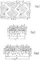
- P type region 3 comprises a peripheral P type frame region 4 of substantially annular shape, and a plurality of elongated P type body stripes 5 substantially parallel to one another (Figs. 1 and 2); body stripes 5 are merged at their ends with the peripheral region 4: thus, body stripes 5 and the frame region 4 forms a signle body region.
- body stripes 5 are separated by elongated insulated gate stripes 6, comprising a gate oxide layer 61 and a polysilicon gate layer 62.
- each body stripe 5 comprises enlarged portions 7 intercalated in a longitudinal direction with narrow portions 8; along a direction transversal to the body stripes 5, the enlarged portions 7 of the body stripes are intercalated with the narrow portions of adjacent body stripes.
- the shape of the body stripes is a consequence of the particular sinuous shape of the insulated gate stripes, because during the manufacturing of the power device the insulated gate stripes are defined first, and the body stripes are then formed in a self-aligned manner with the insulated gate stripes.
- heavily doped source regions 9 of the N type are formed inside the body stripes 5, in such a way as to leave a substantially polygonal portion of body stripe at the center of each enlarged portion 7 of the body stripes 5.
- a dielectric layer 10 shown in dash-and-dot line in Fig. 2 covers all the surface of the chip, and substantially polygonal contact windows 11 are opened thereinto substantially over each enlarged portion 7 of the body stripes 5, so that the source region 9 and the central polygonal portions of the body stripes 5 can be contacted and short-circuited together by a source metallization layer 12.
- the width of the insulated gate stripes 6, the width of the P body stripes 5, the number and size of contact windows, the spacing between contact windows in a same P body stripes are design parameters which can be optimised depending on the desired voltage capability, the manufacturing apparatus and so on.
- the following sizes can be provided:
- Figures 5 and 6 show in top-plan view a second embodiment of the present invention.
- the insulated gate stripes 6 have a slightly different shape with respect to the first embodiment; consequently, also the body stripes 5 have a slightly different shape with respect to the first embodiment.
- each body stripe 5 comprises enlarged portions 7 longitudinally intercalated with narrow portions 8.
- Another difference with respect to the first embodiment is the shape of the source regions 9 inside the body stripes 5: as visible from Figure 6, in this embodiment the source region 9 is interrupted in correspondance of the center of each enlarged portion 7 of the body stripe 5, so as to leave a transversal portion of the body stripe 5 uncovered to allow contact by the superimposed source metallization layer.
- the structure of the present invention can be used for both low and high voltage devices.
- the structure of the present invention can also be used in smart-power technologies, wherein power devices are integrated in a same chip with control logic circuits.
Landscapes
- Metal-Oxide And Bipolar Metal-Oxide Semiconductor Integrated Circuits (AREA)
Priority Applications (1)
| Application Number | Priority Date | Filing Date | Title |
|---|---|---|---|
| EP96410087A EP0823735A1 (de) | 1996-08-05 | 1996-08-05 | MOS-Technologie-Leistungsanordnung |
Applications Claiming Priority (1)
| Application Number | Priority Date | Filing Date | Title |
|---|---|---|---|
| EP96410087A EP0823735A1 (de) | 1996-08-05 | 1996-08-05 | MOS-Technologie-Leistungsanordnung |
Publications (1)
| Publication Number | Publication Date |
|---|---|
| EP0823735A1 true EP0823735A1 (de) | 1998-02-11 |
Family
ID=8225374
Family Applications (1)
| Application Number | Title | Priority Date | Filing Date |
|---|---|---|---|
| EP96410087A Withdrawn EP0823735A1 (de) | 1996-08-05 | 1996-08-05 | MOS-Technologie-Leistungsanordnung |
Country Status (1)
| Country | Link |
|---|---|
| EP (1) | EP0823735A1 (de) |
Cited By (7)
| Publication number | Priority date | Publication date | Assignee | Title |
|---|---|---|---|---|
| WO2001031709A1 (en) * | 1999-10-22 | 2001-05-03 | Semiconductor Components Industries, L.L.C. | Semiconductor device with a single base region and method therefor |
| WO2001031711A3 (en) * | 1999-10-22 | 2001-11-22 | Semiconductor Components Ind | Vertical insulated gate field-effect device and method of making the same |
| US6563170B2 (en) * | 1997-10-22 | 2003-05-13 | Fairchild Korea Semiconductor Ltd. | Insulated gate bipolar transistor |
| WO2006122957A3 (en) * | 2005-05-19 | 2007-02-01 | St Microelectronics Srl | Mos power device with high integration density and manufacturing process thereof |
| WO2013080641A1 (ja) * | 2011-12-01 | 2013-06-06 | 三菱電機株式会社 | 半導体装置 |
| WO2013103051A1 (ja) * | 2012-01-06 | 2013-07-11 | 三菱電機株式会社 | 半導体装置 |
| CN114600249A (zh) * | 2019-11-05 | 2022-06-07 | 赛美科公司 | 具有波形沟道区域的碳化硅平面mosfet |
Citations (6)
| Publication number | Priority date | Publication date | Assignee | Title |
|---|---|---|---|---|
| FR2515429A1 (fr) * | 1981-10-26 | 1983-04-29 | Intersil Inc | Transistor a effet de champ de puissance |
| US4833513A (en) * | 1985-01-20 | 1989-05-23 | Tdk Corporation | MOS FET semiconductor device having a cell pattern arrangement for optimizing channel width |
| JPH01207976A (ja) * | 1988-02-15 | 1989-08-21 | Nec Corp | 半導体装置 |
| US5396097A (en) * | 1993-11-22 | 1995-03-07 | Motorola Inc | Transistor with common base region |
| US5399892A (en) * | 1993-11-29 | 1995-03-21 | Harris Corporation | Mesh geometry for MOS-gated semiconductor devices |
| US5521410A (en) * | 1993-03-22 | 1996-05-28 | Nec Corporation | Power semiconductor device comprising vertical double-diffused MOSFETS each having low on-resistance per unit area |
-
1996
- 1996-08-05 EP EP96410087A patent/EP0823735A1/de not_active Withdrawn
Patent Citations (6)
| Publication number | Priority date | Publication date | Assignee | Title |
|---|---|---|---|---|
| FR2515429A1 (fr) * | 1981-10-26 | 1983-04-29 | Intersil Inc | Transistor a effet de champ de puissance |
| US4833513A (en) * | 1985-01-20 | 1989-05-23 | Tdk Corporation | MOS FET semiconductor device having a cell pattern arrangement for optimizing channel width |
| JPH01207976A (ja) * | 1988-02-15 | 1989-08-21 | Nec Corp | 半導体装置 |
| US5521410A (en) * | 1993-03-22 | 1996-05-28 | Nec Corporation | Power semiconductor device comprising vertical double-diffused MOSFETS each having low on-resistance per unit area |
| US5396097A (en) * | 1993-11-22 | 1995-03-07 | Motorola Inc | Transistor with common base region |
| US5399892A (en) * | 1993-11-29 | 1995-03-21 | Harris Corporation | Mesh geometry for MOS-gated semiconductor devices |
Non-Patent Citations (2)
| Title |
|---|
| BLANCHARD R A: "Zukünftige Entwicklungen bei MOS-Leistungstransistoren", ELEKTRONIK, 4 JUNE 1982, WEST GERMANY, VOL. 31, NR. 11, PAGE(S) 95 - 98, ISSN 0013-5658, XP002019981 * |
| PATENT ABSTRACTS OF JAPAN vol. 013, no. 513 (E - 847) 16 November 1989 (1989-11-16) * |
Cited By (15)
| Publication number | Priority date | Publication date | Assignee | Title |
|---|---|---|---|---|
| US6563170B2 (en) * | 1997-10-22 | 2003-05-13 | Fairchild Korea Semiconductor Ltd. | Insulated gate bipolar transistor |
| WO2001031709A1 (en) * | 1999-10-22 | 2001-05-03 | Semiconductor Components Industries, L.L.C. | Semiconductor device with a single base region and method therefor |
| WO2001031711A3 (en) * | 1999-10-22 | 2001-11-22 | Semiconductor Components Ind | Vertical insulated gate field-effect device and method of making the same |
| US6344379B1 (en) | 1999-10-22 | 2002-02-05 | Semiconductor Components Industries Llc | Semiconductor device with an undulating base region and method therefor |
| WO2006122957A3 (en) * | 2005-05-19 | 2007-02-01 | St Microelectronics Srl | Mos power device with high integration density and manufacturing process thereof |
| JPWO2013080641A1 (ja) * | 2011-12-01 | 2015-04-27 | 三菱電機株式会社 | 半導体装置 |
| US20140299891A1 (en) * | 2011-12-01 | 2014-10-09 | Mitsubishi Electric Corporation | Semiconductor device |
| WO2013080641A1 (ja) * | 2011-12-01 | 2013-06-06 | 三菱電機株式会社 | 半導体装置 |
| US9190468B2 (en) | 2011-12-01 | 2015-11-17 | Mitsubishi Electric Corporation | Semiconductor device |
| WO2013103051A1 (ja) * | 2012-01-06 | 2013-07-11 | 三菱電機株式会社 | 半導体装置 |
| JP5687364B2 (ja) * | 2012-01-06 | 2015-03-18 | 三菱電機株式会社 | 半導体装置 |
| JPWO2013103051A1 (ja) * | 2012-01-06 | 2015-05-11 | 三菱電機株式会社 | 半導体装置 |
| US9324782B2 (en) | 2012-01-06 | 2016-04-26 | Mitsubishi Electric Corporation | Semiconductor device |
| DE112012005591B4 (de) * | 2012-01-06 | 2021-02-11 | Mitsubishi Electric Corporation | Halbleitervorrichtung |
| CN114600249A (zh) * | 2019-11-05 | 2022-06-07 | 赛美科公司 | 具有波形沟道区域的碳化硅平面mosfet |
Similar Documents
| Publication | Publication Date | Title |
|---|---|---|
| US6111297A (en) | MOS-technology power device integrated structure and manufacturing process thereof | |
| US6518127B2 (en) | Trench DMOS transistor having a double gate structure | |
| US5589405A (en) | Method for fabricating VDMOS transistor with improved breakdown characteristics | |
| US7663186B2 (en) | Semiconductor device | |
| US5710455A (en) | Lateral MOSFET with modified field plates and damage areas | |
| US6600182B2 (en) | High current field-effect transistor | |
| US5838042A (en) | DMOS device structure, and related manufacturing process | |
| US20030057478A1 (en) | Mos-gated power semiconductor device | |
| KR100297705B1 (ko) | 낮은 온저항과 높은 항복전압을 갖는 전력용 반도체소자 | |
| US10355132B2 (en) | Power MOSFETs with superior high frequency figure-of-merit | |
| US6867476B2 (en) | Vertical double diffused MOSFET and method of fabricating the same | |
| KR100256387B1 (ko) | 수평 절연 게이트 반도체 장치 | |
| US20050073003A1 (en) | LDMOS transistor | |
| US7276405B2 (en) | Power semiconductor device having high breakdown voltage, low on-resistance and small switching loss and method of forming the same | |
| KR100523118B1 (ko) | 반도체소자 | |
| EP0823735A1 (de) | MOS-Technologie-Leistungsanordnung | |
| US20020113276A1 (en) | High integration density mos technology power device structure | |
| US5291050A (en) | MOS device having reduced gate-to-drain capacitance | |
| KR100529419B1 (ko) | 반도체디바이스 | |
| EP0729186B1 (de) | Leistungsbauelement als integrierte Struktur in MOS-Technologie und Verfahren zu seiner Herstellung | |
| US20240072122A1 (en) | Semiconductor device and method for manufacturing a semiconductor device | |
| EP0780897B1 (de) | Hochgeschwindigkeit-MOS-Technologie-Leistungsanordnung in integrierter Struktur mit reduziertem Gatewiderstand | |
| CN101228636B (zh) | 功率半导体器件以及制造功率半导体器件的方法 | |
| EP0970526A2 (de) | Leistungs-halbleiteranordnungen | |
| US20250040166A1 (en) | Planar JFET Device with Reduced Gate Resistance |
Legal Events
| Date | Code | Title | Description |
|---|---|---|---|
| PUAI | Public reference made under article 153(3) epc to a published international application that has entered the european phase |
Free format text: ORIGINAL CODE: 0009012 |
|
| AK | Designated contracting states |
Kind code of ref document: A1 Designated state(s): DE FR GB IT |
|
| AX | Request for extension of the european patent |
Free format text: AL;LT;LV;SI |
|
| AKX | Designation fees paid |
Free format text: DE FR GB IT |
|
| RBV | Designated contracting states (corrected) |
Designated state(s): DE FR GB IT |
|
| RBV | Designated contracting states (corrected) |
Designated state(s): DE FR GB IT |
|
| RAP3 | Party data changed (applicant data changed or rights of an application transferred) |
Owner name: STMICROELECTRONICS S.A. |
|
| STAA | Information on the status of an ep patent application or granted ep patent |
Free format text: STATUS: THE APPLICATION IS DEEMED TO BE WITHDRAWN |
|
| 18D | Application deemed to be withdrawn |
Effective date: 19980812 |