EP0824603B1 - Vorrichtung zum materialbeschichten grossflächiger substrate - Google Patents
Vorrichtung zum materialbeschichten grossflächiger substrate Download PDFInfo
- Publication number
- EP0824603B1 EP0824603B1 EP96915075A EP96915075A EP0824603B1 EP 0824603 B1 EP0824603 B1 EP 0824603B1 EP 96915075 A EP96915075 A EP 96915075A EP 96915075 A EP96915075 A EP 96915075A EP 0824603 B1 EP0824603 B1 EP 0824603B1
- Authority
- EP
- European Patent Office
- Prior art keywords
- substrate
- evaporation
- source
- movement
- enclosure
- Prior art date
- Legal status (The legal status is an assumption and is not a legal conclusion. Google has not performed a legal analysis and makes no representation as to the accuracy of the status listed.)
- Expired - Lifetime
Links
- 239000000758 substrate Substances 0.000 title claims description 116
- 238000000151 deposition Methods 0.000 title claims description 22
- 239000000463 material Substances 0.000 title claims description 18
- 230000008020 evaporation Effects 0.000 claims description 49
- 238000001704 evaporation Methods 0.000 claims description 49
- 230000008021 deposition Effects 0.000 claims description 14
- 238000000034 method Methods 0.000 claims description 10
- 238000013519 translation Methods 0.000 description 9
- PXHVJJICTQNCMI-UHFFFAOYSA-N Nickel Chemical compound [Ni] PXHVJJICTQNCMI-UHFFFAOYSA-N 0.000 description 6
- 238000004519 manufacturing process Methods 0.000 description 6
- ZOKXTWBITQBERF-UHFFFAOYSA-N Molybdenum Chemical compound [Mo] ZOKXTWBITQBERF-UHFFFAOYSA-N 0.000 description 5
- 230000005465 channeling Effects 0.000 description 5
- 229910052750 molybdenum Inorganic materials 0.000 description 5
- 239000011733 molybdenum Substances 0.000 description 5
- 230000015572 biosynthetic process Effects 0.000 description 3
- 230000007423 decrease Effects 0.000 description 3
- 239000012212 insulator Substances 0.000 description 3
- 229910052759 nickel Inorganic materials 0.000 description 3
- 238000011161 development Methods 0.000 description 2
- 238000009826 distribution Methods 0.000 description 2
- 238000005086 pumping Methods 0.000 description 2
- ZAGHKONXGGSVDV-UHFFFAOYSA-N CCCCC1CCCC1 Chemical compound CCCCC1CCCC1 ZAGHKONXGGSVDV-UHFFFAOYSA-N 0.000 description 1
- 230000001133 acceleration Effects 0.000 description 1
- 230000001154 acute effect Effects 0.000 description 1
- 238000005136 cathodoluminescence Methods 0.000 description 1
- 238000009833 condensation Methods 0.000 description 1
- 230000005494 condensation Effects 0.000 description 1
- 230000001143 conditioned effect Effects 0.000 description 1
- 239000004020 conductor Substances 0.000 description 1
- 238000004090 dissolution Methods 0.000 description 1
- 230000005669 field effect Effects 0.000 description 1
- 238000010438 heat treatment Methods 0.000 description 1
- 238000009776 industrial production Methods 0.000 description 1
- 239000003550 marker Substances 0.000 description 1
- 229910052751 metal Inorganic materials 0.000 description 1
- 239000002184 metal Substances 0.000 description 1
- 229910052758 niobium Inorganic materials 0.000 description 1
- 239000010955 niobium Substances 0.000 description 1
- GUCVJGMIXFAOAE-UHFFFAOYSA-N niobium atom Chemical compound [Nb] GUCVJGMIXFAOAE-UHFFFAOYSA-N 0.000 description 1
- 230000003287 optical effect Effects 0.000 description 1
- 230000003071 parasitic effect Effects 0.000 description 1
- 238000012549 training Methods 0.000 description 1
- 238000011282 treatment Methods 0.000 description 1
- 239000011364 vaporized material Substances 0.000 description 1
- 238000012800 visualization Methods 0.000 description 1
Images


Classifications
-
- H—ELECTRICITY
- H01—ELECTRIC ELEMENTS
- H01J—ELECTRIC DISCHARGE TUBES OR DISCHARGE LAMPS
- H01J9/00—Apparatus or processes specially adapted for the manufacture, installation, removal, maintenance of electric discharge tubes, discharge lamps, or parts thereof; Recovery of material from discharge tubes or lamps
- H01J9/02—Manufacture of electrodes or electrode systems
- H01J9/022—Manufacture of electrodes or electrode systems of cold cathodes
- H01J9/025—Manufacture of electrodes or electrode systems of cold cathodes of field emission cathodes
-
- C—CHEMISTRY; METALLURGY
- C23—COATING METALLIC MATERIAL; COATING MATERIAL WITH METALLIC MATERIAL; CHEMICAL SURFACE TREATMENT; DIFFUSION TREATMENT OF METALLIC MATERIAL; COATING BY VACUUM EVAPORATION, BY SPUTTERING, BY ION IMPLANTATION OR BY CHEMICAL VAPOUR DEPOSITION, IN GENERAL; INHIBITING CORROSION OF METALLIC MATERIAL OR INCRUSTATION IN GENERAL
- C23C—COATING METALLIC MATERIAL; COATING MATERIAL WITH METALLIC MATERIAL; SURFACE TREATMENT OF METALLIC MATERIAL BY DIFFUSION INTO THE SURFACE, BY CHEMICAL CONVERSION OR SUBSTITUTION; COATING BY VACUUM EVAPORATION, BY SPUTTERING, BY ION IMPLANTATION OR BY CHEMICAL VAPOUR DEPOSITION, IN GENERAL
- C23C14/00—Coating by vacuum evaporation, by sputtering or by ion implantation of the coating forming material
- C23C14/22—Coating by vacuum evaporation, by sputtering or by ion implantation of the coating forming material characterised by the process of coating
- C23C14/24—Vacuum evaporation
- C23C14/243—Crucibles for source material
-
- C—CHEMISTRY; METALLURGY
- C23—COATING METALLIC MATERIAL; COATING MATERIAL WITH METALLIC MATERIAL; CHEMICAL SURFACE TREATMENT; DIFFUSION TREATMENT OF METALLIC MATERIAL; COATING BY VACUUM EVAPORATION, BY SPUTTERING, BY ION IMPLANTATION OR BY CHEMICAL VAPOUR DEPOSITION, IN GENERAL; INHIBITING CORROSION OF METALLIC MATERIAL OR INCRUSTATION IN GENERAL
- C23C—COATING METALLIC MATERIAL; COATING MATERIAL WITH METALLIC MATERIAL; SURFACE TREATMENT OF METALLIC MATERIAL BY DIFFUSION INTO THE SURFACE, BY CHEMICAL CONVERSION OR SUBSTITUTION; COATING BY VACUUM EVAPORATION, BY SPUTTERING, BY ION IMPLANTATION OR BY CHEMICAL VAPOUR DEPOSITION, IN GENERAL
- C23C14/00—Coating by vacuum evaporation, by sputtering or by ion implantation of the coating forming material
- C23C14/22—Coating by vacuum evaporation, by sputtering or by ion implantation of the coating forming material characterised by the process of coating
- C23C14/50—Substrate holders
- C23C14/505—Substrate holders for rotation of the substrates
Definitions
- the present invention relates in a way general to the deposition of material by evaporation on a large substrate.
- An application is the realization of microtip electron sources using electronic emission by field effect, said sources being large.
- These electron sources are, for example, used in visualization devices by cathodoluminescence excited by field emission, and especially in large flat screens (of the order of a square meter).
- Figure 1 shows an already developed structure, comprising on a substrate 6 surmounted by an insulator 7, a cathode conductor system 8, a layer resistive 9, grids 10a superimposed in the form crossed with an intermediate insulator 12 and a layer 23, for example nickel, deposited on the surface for serve as a mask during the operations of making microtips.
- This layer 23 of nickel, the grids 10a and the insulator 12 are drilled with holes 16 in the background of which it is a question of coming to deposit the futures microtips made of a conductive metal in electrical connection with the cathode electrode 8 to through the resistive layer 9.
- the deposition step of the molybdenum layer 18a is conventionally carried out by evaporation of molybdenum heated in a crucible and condensation of steam from molybdenum on the substrate covered with the structure stacked 7, 8, 9, 12, 10a and 23, pierced with holes 16.
- FIG. 4 A conventional evaporator is illustrated in FIG. 4.
- the material to be evaporated is heated in a source crucible 30.
- the substrates 33-1, 33-2, 33-3 are positioned on a substrate holder 31 and rotated on them- same, around an axis 34-1, 34-2, 34-3.
- the substrate holder 31 is placed opposite the crucible 30 and it is itself rotated about the axis 34-2. Evaporation takes place under vacuum at around 10 -5 -10 -6 mbar in an enclosure 35 pumped by a suitable pumping system 36.
- the substrate holder 31 has a shape adapted so that the substrates 33 receive the vapor in quasi-normal incidence with a maximum angle ⁇ max .
- This device is well suited for carrying out deposits on small or medium-sized substrates (at most a few tens of cm).
- the angle of incidence of the vapor ⁇ being very small (a few degrees), it is almost impossible to envisage depositing on a substrate a diagonal meter, the deposition speed being much too weak for an industrial process.
- the document FR-2 701 601 describes a first device for producing microtip sources, also called "ICB device”.
- a crucible is heated by a heating element and the vaporized material is then partially ionized, which leads to the formation of clusters which are accelerated.
- This type of device is not suitable for depositing on large substrates area.
- a second device includes a crucible with a plurality of nozzles through which a vapor is discharged into a vacuum box, in which it is ionized then accelerated.
- this document proposes to increase the ratio L / r where L is the thickness of the crucible and r the diameter of the nozzles.
- this type of device is incompatible with industrial production, especially on large substrates.
- the nozzles can be gradually blocked by parasitic deposits of matter. If the L / r ratio is increased, in order to increase the directivity, this problem becomes even more acute, since the vapors pass through the nozzles over a longer length important, while the latter have a diameter weaker. This also results in variations in flow rate of evaporated material.
- the object of the invention is to resolve the above problem, that is to say to offer a simple device for depositing on large surface substrates, and allowing maintain an angle of incidence of the vapor relatively small and sufficient deposition rate for an industrial process.
- the sources are placed directly opposite of the substrate: they see the substrate directly or a portion of it.
- Means for channeling the vapors emitted can be covers or walls separating the sources each other.
- the caches form compartments inside the enclosure, each source of evaporation being arranged in a compartment.
- These covers or walls can be vertical.
- the covers or walls can form cells having, at least in part, a frustoconical shape.
- a substrate holder allows mount a substrate near one end of the walls.
- a subproblem is to improve the consistency of the deposit on the substrate.
- These consistency issues may in particular appear due to the means of vapor channeling.
- these means have the form of covers or walls, marks defining areas masked by these means can appear on the substrate.
- Non-uniformity can also be due to varying deposition rates from one point to another on the substrate.
- a device comprises in in addition to means for moving the substrate, so as to pass different parts of the substrate successively before the different sources.
- These means can be means for generate and / or combine rotational movements and / or translation in a plane.
- the movement can be a planetary rotation movement of the substrate.
- a combined movement of rotation and translation around an axis, called the central axis of the evaporation system, allows to limit advantageously the lateral dimensions of the system evaporation. Indeed, in this case, the total area described by the substrate is minimized.
- Such movement can be ensured by a two interlocking gears system rotating in one same plane and around a fixed gear.
- the movement is provided by a gear kept at a constant distance from a wheel fixed tooth, a toothed belt or a chain surrounding the fixed gear and the gear.
- the means for channeling the vapors emitted by each source define, with this source, a cell, the surface swept by the moving substrate in this cell presenting, in a plane perpendicular to the direction of evaporation in this cell, a center of symmetry, the source being placed on an axis perpendicular to the surface swept by the substrate and passing through this center of symmetry.
- the substrate is a substrate of a microtip emissive system, the microtips being carried out by the evaporation step.
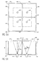
- FIG. 5A and 5B respectively represent a view of above and a sectional view of a device according to the invention.
- This device essentially consists of an enclosure 43 which, in the example illustrated in the figures, has an approximately square section. This enclosure is delimited by walls 52, 53, ..., 59. This enclosure is divided into four compartments by walls 48, 49, 50, 51. At the bottom of each of these compartments is a source of evaporation 40 , 42, 44, 46. A surface or substrate 60 can be introduced into the top of the enclosure 43, and mounted on a substrate holder (not shown in the figure) so that the deposition surface is located a distance h from the bottom of the enclosure 43. The presence of the various vertical walls makes it possible to prevent material from being evaporated on the surface of the substrate with an angle greater than the angle ⁇ 0 shown in FIG. 5B.
- the above example is limited to four sources evaporation. It is also possible to realize an enclosure 43 comprising two, three, five or more five sources of evaporation, as required. Through elsewhere, the enclosure 43 is equipped with a device for pumping (not shown in the figures) allowing to ensure a certain vacuum during the operation evaporation.
- the enclosure which has been described presents vertical walls, arranged perpendicularly between them and defining the compartments approximately cubic. It is clear that the dimensions of the different walls can be as well as the distribution of the compartments to inside the same volume of an enclosure. So, we shown in Figures 6A, 6B, 6C different possible speaker shapes and different possible wall distributions inside the enclosure.
- Figure 6A is a top view of a enclosure 62 having a substantially external shape identical to that of enclosure 43 of FIGS. 5A and 5B. Inside, walls 64, 66 are arranged in diagonal, a source of evaporation being arranged at the bottom of each of the four compartments as well delimited. Eight compartments can be made in introducing additional walls 68, 70, and four additional sources of evaporation.
- the device of FIG. 6B comprises an enclosure having overall the shape of a cylinder 72 and a certain number of walls 74, 76, 78, 80 delimiting sectors cylindrical inside the enclosure 72. A source at the bottom of each sector cylindrical.
- FIG. 6C represents an enclosure with inside which compartments 82, 84, 86, 88 of frustoconical shape are made, the different walls inside the enclosure no longer arranged vertically as in the examples previous.
- the walls delimiting compartments inside the enclosure can form cells with a cylindrical symmetry with polygonal base (this is the case Figures 5A, 6A, 6B) or cells having a partially frustoconical shape.
- Each source is located inside a compartment.
- Each compartment has an opening 61, 63 ( Figure 5B), 65, 67, 69, 71 ( Figure 6C) near which is the substrate.
- the substrate is located near one end of the walls.
- uniformity may be due to deposition speed differences between different points of a same substrate.
- this deposit speed gap can be a real problem since the total deposit time will be conditioned by the time required to cover areas where speed deposit is the lowest. This has the consequence increased manufacturing time and wastage of a lot of evaporated material. The latter is found then in overthickness in high speed areas deposit and on the walls of the evaporation system.
- the uniformity therefore varies as the cos n + 3 ⁇ of the angle ⁇ of evaporation.
- This movement improves the uniformity of deposit while limiting the lateral dimensions of the system. On the other hand, it helps prevent areas masked by the caches on the substrate.
- a substrate 112 of shape approximately square, is arranged so asymmetrical compared to the different compartments.
- the planetary movement of the substrate is a combination of a rotational movement of the substrate around the central axis of the system and a movement of rotation of the substrate around an axis perpendicular to its plan (passing for example through its center symmetry, if the substrate has such a center of symmetry).
- the substrate holder 99 is fixed on a gear represented in FIG. 8C by the reference 97 so that, for example, the center of the substrate C ( Figure 8A) coincides with the center (axis) of this gear.
- a fixed gear 96 of the same diameter that this gear 97 and having the same number of teeth and the same pitch between the teeth is fixed on axis 102 of the evaporation system.
- a second gear 95 having the same pitch between the teeth, connects the center gear C to the fixed gear of center O.
- the two gears 95 and 97 are connected to a support arm 98, for example, using bearings balls, to ensure their mobility.
- This support arm 98 rotates around the axis of the fixed gear 96, training 100 will be done for example using a engine.
- This system therefore allows to rotate-translate the substrate 112 around the center O of the evaporation system.
- Any other mechanical system can be used, which allows to obtain the same movement; for example as illustrated in FIG. 8E, it is possible to delete the gear 95 of Figures 8C and 8D and replace with a toothed belt 105 which surrounds the fixed gear 96 and gear 97.
- each source of evaporation in each compartment on an axis perpendicular to the surface to be coated and passing through this center of symmetry.
- the uniformity of the deposit can be calculated by summing the contributions of four sources of evaporation on the substrate. We calculates for example the ratio between the average speed of deposit at a point and the average speed of deposit at center of the square substrate.
- Figures 9 to 11 correspond to a substrate still and serve as a reference for comparison.
- the height of the system remains small in comparison with the 3.16m of the prior art system ( Figure 4), value which has been calculated in the introduction to this application.
- the value of h varies from lm to 2m in the examples given, depending on the configuration (angle ⁇ and distance OC). This range of heights (1-2 meters) is quite made acceptable to those skilled in the art, the limitation is located around 2 meters in height. He will be of course better to minimize this height, for example by accepting a higher tolerance large on the angle ⁇ (for example up to 15 °).
- microdot repositories to make sources of electrons, for example a source such as that described above, in conjunction with Figures 1 to 3.
- the invention therefore also relates to a method to deposit on large surfaces, this process of introducing the surface, or substrate, in a device as described above, according to the invention.
- a substrate into the evaporation device having the structure described above in connection with the figure 1.
Landscapes
- Chemical & Material Sciences (AREA)
- Engineering & Computer Science (AREA)
- Chemical Kinetics & Catalysis (AREA)
- Materials Engineering (AREA)
- Mechanical Engineering (AREA)
- Metallurgy (AREA)
- Organic Chemistry (AREA)
- Manufacturing & Machinery (AREA)
- Physical Vapour Deposition (AREA)
Claims (12)
- Vorrichtung zum Materialbeschichten eines Substrats (60, 90, 112) durch Aufdampfen,
dadurch gekennzeichnet, daß sie umfaßt:einen Behälter (43, 62, 72), in dem sich die Verdampfungsquellen (40, 42, 44, 46) des Materials befinden, n an der Zahl,Einrichtungen (48-51, 64, 66, 68, 70, 74, 76, 78, 80), um die von den genannten Quellen entwickelten Dämpfe während des Aufdampfens in Richtung Substrat zu kanalisieren, wobei diese Einrichtungen gebildet werden durch Wände oder Abteilungen, die im Innern des Behälters Abteile bilden, und jede Verdampfungsquelle in einem Abteil angeordnet ist. - Vorrichtung nach Anspruch 1, wobei die Abteilungen oder Wände senkrecht sind.
- Vorrichtung nach Anspruch 1, wobei die Abteilungen oder Wände Zellen bilden, die wenigstens teilweise eine kegelstumpfartige Struktur haben.
- Vorrichtung nach einem der Ansprüche 1 bis 3, wobei sie außerdem Einrichtungen (94-100) zum Bewegen eines Substrats umfaßt, sodaß verschiedene Teile des Substrats nacheinander an verschiedenen Quellen verbeigeführt werden.
- Vorrichtung nach Anspruch 4, wobei die Bewegungseinrichtungen (94-100) Einrichtungen zum Erzeugen und/oder Kombinieren von Rotations- und/oder Translationsbewegungen in einer Ebene sind.
- Vorrichtung nach Anspruch 5, wobei die Bewegung eine planetarische Rotationsbewegung des Substrats um sich selbst ist.
- Vorrichtung nach Anspruch 5, wobei die Bewegung eine Rotations-Translationsbewegung des Substrats ist.
- Vorrichtung nach Anspruch 7, wobei die Bewegung gewährleistet wird durch ein System ineinandergreifender Zahnräder, wobei sich zwei Zahnräder (95, 97) in derselben Ebene und um ein feststehendes Zahnrad (96) herum drehen.
- Vorrichtung nach Anspruch 7, wobei die Bewegung durch ein Zahnrad (97) gewährleistet wird, das in einem konstanten Abstand von einem Zahnrad (96) gehalten wird, wobei ein Zahnriemen (105) oder eine Kette das feststehende Zahnrad (96) und das Zahnrad (97) umgibt.
- Vorrichtung nach Anspruch 4, wobei die Einrichtungen zum Kanalisieren der durch jede Quelle entwickelten Dämpfe mit dieser Quelle eine Zelle abgrenzen, die durch das sich bewegende Substrat in dieser Zelle bestrichene Fläche in einer zur Aufdampfrichtung in dieser Zelle senkrechten Ebene ein Symmetriezentrum aufweist und die Quelle sich in einer Achse befindet, die zu der durch das Substrat bestrichenen Fläche senkrecht ist und dieses Symmetriezentrum durchläuft.
- Beschichtungsverfahren durch Aufdampfen eines Materials auf ein Substrat, dadurch gekennzeichnet, daß man das Substrat in einen Behälter einer Vorrichtung nach einem der Ansprüche 1 bis 10 gibt und anschließend das Aufdampfen durchführt.
- Verfahren nach Anspruch 11, wobei das Substrat ein Substrat für Mikrospitzen-Elektronenquellen ist.
Applications Claiming Priority (3)
| Application Number | Priority Date | Filing Date | Title |
|---|---|---|---|
| FR9504873A FR2733253B1 (fr) | 1995-04-24 | 1995-04-24 | Dispositif pour deposer un materiau par evaporation sur des substrats de grande surface |
| FR9504873 | 1995-04-24 | ||
| PCT/FR1996/000616 WO1996034123A1 (fr) | 1995-04-24 | 1996-04-23 | Dispositif pour deposer un materiau par evaporation sur des substrats de grande surface |
Publications (2)
| Publication Number | Publication Date |
|---|---|
| EP0824603A1 EP0824603A1 (de) | 1998-02-25 |
| EP0824603B1 true EP0824603B1 (de) | 1999-06-30 |
Family
ID=9478388
Family Applications (1)
| Application Number | Title | Priority Date | Filing Date |
|---|---|---|---|
| EP96915075A Expired - Lifetime EP0824603B1 (de) | 1995-04-24 | 1996-04-23 | Vorrichtung zum materialbeschichten grossflächiger substrate |
Country Status (6)
| Country | Link |
|---|---|
| US (1) | US6509061B1 (de) |
| EP (1) | EP0824603B1 (de) |
| JP (1) | JP4072570B2 (de) |
| DE (1) | DE69603079T2 (de) |
| FR (1) | FR2733253B1 (de) |
| WO (1) | WO1996034123A1 (de) |
Families Citing this family (11)
| Publication number | Priority date | Publication date | Assignee | Title |
|---|---|---|---|---|
| CA2185640A1 (en) * | 1995-11-30 | 1997-05-31 | Russell J. Hill | Electron beam evaporation apparatus and method |
| US6592675B2 (en) | 2001-08-09 | 2003-07-15 | Moore Epitaxial, Inc. | Rotating susceptor |
| WO2004090928A1 (ja) * | 2003-04-04 | 2004-10-21 | Matsushita Electric Industrial Co. Ltd. | プラズマディスプレイパネルの製造方法 |
| KR100637180B1 (ko) * | 2004-11-05 | 2006-10-23 | 삼성에스디아이 주식회사 | 증착 방법 및 이를 위한 증착 장치 |
| US20100247747A1 (en) * | 2009-03-27 | 2010-09-30 | Semiconductor Energy Laboratory Co., Ltd. | Film Deposition Apparatus, Method for Depositing Film, and Method for Manufacturing Lighting Device |
| SG175247A1 (en) * | 2009-04-28 | 2011-11-28 | Ferrotec Usa Corp | Lift-off deposition system featuring a density optimized hula substrate holder in a conical dep0sition chamber |
| KR20120138305A (ko) * | 2011-06-14 | 2012-12-26 | 삼성디스플레이 주식회사 | 유기 박막 증착 시스템 및 유기 박막 증착 방법 |
| JP2013137379A (ja) * | 2011-12-28 | 2013-07-11 | Dainippon Printing Co Ltd | フレネルレンズシートに対する蒸着方法、反射スクリーンの製造方法 |
| HK1215127A2 (zh) | 2015-06-17 | 2016-08-12 | Master Dynamic Limited | 制品涂层的设备、仪器和工艺 |
| CN105088145B (zh) * | 2015-08-19 | 2017-03-29 | 京东方科技集团股份有限公司 | 用于oled蒸发源的坩埚及其制造方法 |
| JP2017173742A (ja) * | 2016-03-25 | 2017-09-28 | 大日本印刷株式会社 | 偏光子の製造方法 |
Family Cites Families (17)
| Publication number | Priority date | Publication date | Assignee | Title |
|---|---|---|---|---|
| US3244557A (en) * | 1963-09-19 | 1966-04-05 | Ibm | Process of vapor depositing and annealing vapor deposited layers of tin-germanium and indium-germanium metastable solid solutions |
| US3853091A (en) * | 1973-12-03 | 1974-12-10 | Ibm | Thin film coating apparatus |
| US4681773A (en) * | 1981-03-27 | 1987-07-21 | American Telephone And Telegraph Company At&T Bell Laboratories | Apparatus for simultaneous molecular beam deposition on a plurality of substrates |
| US4646680A (en) * | 1985-12-23 | 1987-03-03 | General Electric Company | Crucible for use in molecular beam epitaxial processing |
| FR2593953B1 (fr) | 1986-01-24 | 1988-04-29 | Commissariat Energie Atomique | Procede de fabrication d'un dispositif de visualisation par cathodoluminescence excitee par emission de champ |
| JPH0745711B2 (ja) * | 1987-12-10 | 1995-05-17 | 株式会社日立製作所 | 高指向性蒸着装置 |
| US5133286A (en) * | 1989-04-14 | 1992-07-28 | Samsung Electro-Mechanics Co., Ltd. | Substrate-heating device and boat structure for a vacuum-depositing apparatus |
| JPH03134164A (ja) * | 1989-10-18 | 1991-06-07 | Ricoh Co Ltd | 薄膜形成装置及びこの装置を用いた超伝導薄膜形成方法 |
| FR2663462B1 (fr) | 1990-06-13 | 1992-09-11 | Commissariat Energie Atomique | Source d'electrons a cathodes emissives a micropointes. |
| DE4025659A1 (de) * | 1990-08-14 | 1992-02-20 | Leybold Ag | Umlaufraedergetriebe mit einem raedersatz, insbesondere fuer vorrichtungen zum beschichten von substraten |
| JPH04285157A (ja) * | 1991-03-12 | 1992-10-09 | Hitachi Ltd | 金属の蒸発方法 |
| DE4123342C2 (de) * | 1991-07-15 | 1999-08-19 | Leybold Ag | Reihenverdampfer für Vakuumbedampfungsanlagen |
| JP3134164B2 (ja) | 1991-07-31 | 2001-02-13 | 京セラ株式会社 | 留守番電話機の録音再生方式 |
| US5334302A (en) * | 1991-11-15 | 1994-08-02 | Tokyo Electron Limited | Magnetron sputtering apparatus and sputtering gun for use in the same |
| US5344352A (en) * | 1992-04-02 | 1994-09-06 | U.S. Philips Corporation | Method of manufacturing a pointed electrode, and device for using said method |
| US5584739A (en) * | 1993-02-10 | 1996-12-17 | Futaba Denshi Kogyo K.K | Field emission element and process for manufacturing same |
| US5518548A (en) * | 1995-08-03 | 1996-05-21 | Honeywell Inc. | Deposition barrier |
-
1995
- 1995-04-24 FR FR9504873A patent/FR2733253B1/fr not_active Expired - Fee Related
-
1996
- 1996-04-23 DE DE69603079T patent/DE69603079T2/de not_active Expired - Lifetime
- 1996-04-23 US US08/931,000 patent/US6509061B1/en not_active Expired - Fee Related
- 1996-04-23 EP EP96915075A patent/EP0824603B1/de not_active Expired - Lifetime
- 1996-04-23 WO PCT/FR1996/000616 patent/WO1996034123A1/fr not_active Ceased
- 1996-04-23 JP JP53221596A patent/JP4072570B2/ja not_active Expired - Fee Related
Also Published As
| Publication number | Publication date |
|---|---|
| EP0824603A1 (de) | 1998-02-25 |
| US6509061B1 (en) | 2003-01-21 |
| JPH11504077A (ja) | 1999-04-06 |
| FR2733253B1 (fr) | 1997-06-13 |
| DE69603079D1 (de) | 1999-08-05 |
| DE69603079T2 (de) | 2000-03-16 |
| FR2733253A1 (fr) | 1996-10-25 |
| JP4072570B2 (ja) | 2008-04-09 |
| WO1996034123A1 (fr) | 1996-10-31 |
Similar Documents
| Publication | Publication Date | Title |
|---|---|---|
| EP0234989B1 (de) | Herstellungsverfahren einer feldeffektangeregten Kathodenlumineszenz-Wiedergabevorrichtung | |
| EP0824603B1 (de) | Vorrichtung zum materialbeschichten grossflächiger substrate | |
| EP2390689A1 (de) | Optische Filter für Strahlen mit variablen Einfallwinkeln und Detektor mit einen solchen Filter | |
| EP0696045B1 (de) | Kathode eines flachen Bildschirmes mit konstantem Zugriffswiderstand | |
| EP2267893B1 (de) | Volumenwellenresonator mit teilweise gefüllten Kavitäten | |
| EP0707237B1 (de) | Verfahren zur Herstellung von Löchern in Photoresistschichten, Anwendung für die Herstellung von Elektronenquelle mit Mikrospitzenemissionskathoden und flachen Bildschirmen | |
| FR2963476A1 (fr) | Procede de realisation d'un condensateur comprenant un reseau de nano-capacites | |
| EP0550335B1 (de) | Einrichtung zum Steuern der Form eines Strahles geladener Teilchen | |
| FR2707795A1 (fr) | Perfectionnement à un procédé de fabrication d'une source d'électrons à micropointes. | |
| FR2952473A1 (fr) | Procede de realisation d'un circuit courbe | |
| EP3788674A1 (de) | Breitbanddrahtantenne | |
| FR2735900A1 (fr) | Source d'electrons du type a emission de champ et procede pour la fabriquer | |
| FR2748847A1 (fr) | Procede de fabrication d'une cathode froide a emission de champ | |
| FR2779271A1 (fr) | Procede de fabrication d'une source d'electrons a micropointes, a grille de focalisation auto-alignee | |
| EP0674804B1 (de) | Beschichtungsvorrichtung zum aufdampfen von metallischem material auf ein substrat | |
| FR2756969A1 (fr) | Ecran d'affichage comprenant une source d'electrons a micropointes, observable a travers le support des micropointes, et procede de fabrication de cette source | |
| FR2917191A1 (fr) | Dispositif d'eclairage pour ecran a cristal liquide | |
| EP2887360B1 (de) | Messung der Auflösung eines Röntgenstrahlabbildungssystems | |
| EP0709741B1 (de) | Photolithographisches Verfahren zur Herstellung von kreisförmigen Strukturen mit hoher Dichte | |
| FR2758206A1 (fr) | Procede de fabrication d'une cathode a emission de champ | |
| FR2573548A1 (fr) | Dispositif pour le depot d'une couche d'orientation d'une cellule a cristal liquide | |
| EP3537489B1 (de) | Herstellungsverfahren einer durchlaufenden vorrichtung | |
| EP1168405A2 (de) | Werkzeug, mit dem Abstandshalter in einer flachen Anzeigetafel montiert werden | |
| WO2022175618A1 (fr) | Dispositif pyroelectrique comprenant un substrat a couche superficielle pyroelectrique et procede de realisation | |
| EP1000434A1 (de) | Verfahren zur erlangung von automatisch ausgerichteten öffnungen, insbesondere zur fokussierelektrode für einen flachen mikrospitzen-bildschirm |
Legal Events
| Date | Code | Title | Description |
|---|---|---|---|
| PUAI | Public reference made under article 153(3) epc to a published international application that has entered the european phase |
Free format text: ORIGINAL CODE: 0009012 |
|
| 17P | Request for examination filed |
Effective date: 19970916 |
|
| AK | Designated contracting states |
Kind code of ref document: A1 Designated state(s): DE GB IT |
|
| GRAG | Despatch of communication of intention to grant |
Free format text: ORIGINAL CODE: EPIDOS AGRA |
|
| GRAG | Despatch of communication of intention to grant |
Free format text: ORIGINAL CODE: EPIDOS AGRA |
|
| GRAH | Despatch of communication of intention to grant a patent |
Free format text: ORIGINAL CODE: EPIDOS IGRA |
|
| 17Q | First examination report despatched |
Effective date: 19980630 |
|
| GRAH | Despatch of communication of intention to grant a patent |
Free format text: ORIGINAL CODE: EPIDOS IGRA |
|
| GRAA | (expected) grant |
Free format text: ORIGINAL CODE: 0009210 |
|
| AK | Designated contracting states |
Kind code of ref document: B1 Designated state(s): DE GB IT |
|
| REF | Corresponds to: |
Ref document number: 69603079 Country of ref document: DE Date of ref document: 19990805 |
|
| ITF | It: translation for a ep patent filed | ||
| GBT | Gb: translation of ep patent filed (gb section 77(6)(a)/1977) |
Effective date: 19990903 |
|
| PLBE | No opposition filed within time limit |
Free format text: ORIGINAL CODE: 0009261 |
|
| STAA | Information on the status of an ep patent application or granted ep patent |
Free format text: STATUS: NO OPPOSITION FILED WITHIN TIME LIMIT |
|
| 26N | No opposition filed | ||
| REG | Reference to a national code |
Ref country code: GB Ref legal event code: IF02 |
|
| PGFP | Annual fee paid to national office [announced via postgrant information from national office to epo] |
Ref country code: IT Payment date: 20070522 Year of fee payment: 12 |
|
| PG25 | Lapsed in a contracting state [announced via postgrant information from national office to epo] |
Ref country code: IT Free format text: LAPSE BECAUSE OF NON-PAYMENT OF DUE FEES Effective date: 20080423 |
|
| PGFP | Annual fee paid to national office [announced via postgrant information from national office to epo] |
Ref country code: GB Payment date: 20120327 Year of fee payment: 17 |
|
| PGFP | Annual fee paid to national office [announced via postgrant information from national office to epo] |
Ref country code: DE Payment date: 20120430 Year of fee payment: 17 |
|
| GBPC | Gb: european patent ceased through non-payment of renewal fee |
Effective date: 20130423 |
|
| PG25 | Lapsed in a contracting state [announced via postgrant information from national office to epo] |
Ref country code: DE Free format text: LAPSE BECAUSE OF NON-PAYMENT OF DUE FEES Effective date: 20131101 Ref country code: GB Free format text: LAPSE BECAUSE OF NON-PAYMENT OF DUE FEES Effective date: 20130423 |
|
| REG | Reference to a national code |
Ref country code: DE Ref legal event code: R119 Ref document number: 69603079 Country of ref document: DE Effective date: 20131101 |