EP0825689A2 - Dispositif optique à l'émission de lumière polarisée commutable, transmetteur optique utilisant ce dispositif, et méthode de commutation d'un dispositif optique - Google Patents
Dispositif optique à l'émission de lumière polarisée commutable, transmetteur optique utilisant ce dispositif, et méthode de commutation d'un dispositif optique Download PDFInfo
- Publication number
- EP0825689A2 EP0825689A2 EP97114493A EP97114493A EP0825689A2 EP 0825689 A2 EP0825689 A2 EP 0825689A2 EP 97114493 A EP97114493 A EP 97114493A EP 97114493 A EP97114493 A EP 97114493A EP 0825689 A2 EP0825689 A2 EP 0825689A2
- Authority
- EP
- European Patent Office
- Prior art keywords
- light
- resonator structure
- resonance
- diffraction grating
- optical device
- Prior art date
- Legal status (The legal status is an assumption and is not a legal conclusion. Google has not performed a legal analysis and makes no representation as to the accuracy of the status listed.)
- Withdrawn
Links
Images


Classifications
-
- H—ELECTRICITY
- H01—ELECTRIC ELEMENTS
- H01S—DEVICES USING THE PROCESS OF LIGHT AMPLIFICATION BY STIMULATED EMISSION OF RADIATION [LASER] TO AMPLIFY OR GENERATE LIGHT; DEVICES USING STIMULATED EMISSION OF ELECTROMAGNETIC RADIATION IN WAVE RANGES OTHER THAN OPTICAL
- H01S5/00—Semiconductor lasers
- H01S5/10—Construction or shape of the optical resonator, e.g. extended or external cavity, coupled cavities, bent-guide, varying width, thickness or composition of the active region
- H01S5/1028—Coupling to elements in the cavity, e.g. coupling to waveguides adjacent the active region, e.g. forward coupled [DFC] structures
- H01S5/1032—Coupling to elements comprising an optical axis that is not aligned with the optical axis of the active region
-
- B—PERFORMING OPERATIONS; TRANSPORTING
- B82—NANOTECHNOLOGY
- B82Y—SPECIFIC USES OR APPLICATIONS OF NANOSTRUCTURES; MEASUREMENT OR ANALYSIS OF NANOSTRUCTURES; MANUFACTURE OR TREATMENT OF NANOSTRUCTURES
- B82Y20/00—Nanooptics, e.g. quantum optics or photonic crystals
-
- H—ELECTRICITY
- H01—ELECTRIC ELEMENTS
- H01S—DEVICES USING THE PROCESS OF LIGHT AMPLIFICATION BY STIMULATED EMISSION OF RADIATION [LASER] TO AMPLIFY OR GENERATE LIGHT; DEVICES USING STIMULATED EMISSION OF ELECTROMAGNETIC RADIATION IN WAVE RANGES OTHER THAN OPTICAL
- H01S5/00—Semiconductor lasers
- H01S5/06—Arrangements for controlling the laser output parameters, e.g. by operating on the active medium
- H01S5/062—Arrangements for controlling the laser output parameters, e.g. by operating on the active medium by varying the potential of the electrodes
- H01S5/0625—Arrangements for controlling the laser output parameters, e.g. by operating on the active medium by varying the potential of the electrodes in multi-section lasers
-
- H—ELECTRICITY
- H01—ELECTRIC ELEMENTS
- H01S—DEVICES USING THE PROCESS OF LIGHT AMPLIFICATION BY STIMULATED EMISSION OF RADIATION [LASER] TO AMPLIFY OR GENERATE LIGHT; DEVICES USING STIMULATED EMISSION OF ELECTROMAGNETIC RADIATION IN WAVE RANGES OTHER THAN OPTICAL
- H01S5/00—Semiconductor lasers
- H01S5/10—Construction or shape of the optical resonator, e.g. extended or external cavity, coupled cavities, bent-guide, varying width, thickness or composition of the active region
- H01S5/12—Construction or shape of the optical resonator, e.g. extended or external cavity, coupled cavities, bent-guide, varying width, thickness or composition of the active region the resonator having a periodic structure, e.g. in distributed feedback [DFB] lasers
-
- H—ELECTRICITY
- H01—ELECTRIC ELEMENTS
- H01S—DEVICES USING THE PROCESS OF LIGHT AMPLIFICATION BY STIMULATED EMISSION OF RADIATION [LASER] TO AMPLIFY OR GENERATE LIGHT; DEVICES USING STIMULATED EMISSION OF ELECTROMAGNETIC RADIATION IN WAVE RANGES OTHER THAN OPTICAL
- H01S5/00—Semiconductor lasers
- H01S5/06—Arrangements for controlling the laser output parameters, e.g. by operating on the active medium
- H01S5/062—Arrangements for controlling the laser output parameters, e.g. by operating on the active medium by varying the potential of the electrodes
- H01S5/06203—Transistor-type lasers
-
- H—ELECTRICITY
- H01—ELECTRIC ELEMENTS
- H01S—DEVICES USING THE PROCESS OF LIGHT AMPLIFICATION BY STIMULATED EMISSION OF RADIATION [LASER] TO AMPLIFY OR GENERATE LIGHT; DEVICES USING STIMULATED EMISSION OF ELECTROMAGNETIC RADIATION IN WAVE RANGES OTHER THAN OPTICAL
- H01S5/00—Semiconductor lasers
- H01S5/06—Arrangements for controlling the laser output parameters, e.g. by operating on the active medium
- H01S5/062—Arrangements for controlling the laser output parameters, e.g. by operating on the active medium by varying the potential of the electrodes
- H01S5/06233—Controlling other output parameters than intensity or frequency
- H01S5/06236—Controlling other output parameters than intensity or frequency controlling the polarisation, e.g. TM/TE polarisation switching
-
- H—ELECTRICITY
- H01—ELECTRIC ELEMENTS
- H01S—DEVICES USING THE PROCESS OF LIGHT AMPLIFICATION BY STIMULATED EMISSION OF RADIATION [LASER] TO AMPLIFY OR GENERATE LIGHT; DEVICES USING STIMULATED EMISSION OF ELECTROMAGNETIC RADIATION IN WAVE RANGES OTHER THAN OPTICAL
- H01S5/00—Semiconductor lasers
- H01S5/10—Construction or shape of the optical resonator, e.g. extended or external cavity, coupled cavities, bent-guide, varying width, thickness or composition of the active region
- H01S5/1021—Coupled cavities
-
- H—ELECTRICITY
- H01—ELECTRIC ELEMENTS
- H01S—DEVICES USING THE PROCESS OF LIGHT AMPLIFICATION BY STIMULATED EMISSION OF RADIATION [LASER] TO AMPLIFY OR GENERATE LIGHT; DEVICES USING STIMULATED EMISSION OF ELECTROMAGNETIC RADIATION IN WAVE RANGES OTHER THAN OPTICAL
- H01S5/00—Semiconductor lasers
- H01S5/10—Construction or shape of the optical resonator, e.g. extended or external cavity, coupled cavities, bent-guide, varying width, thickness or composition of the active region
- H01S5/1028—Coupling to elements in the cavity, e.g. coupling to waveguides adjacent the active region, e.g. forward coupled [DFC] structures
- H01S5/1032—Coupling to elements comprising an optical axis that is not aligned with the optical axis of the active region
- H01S5/1035—Forward coupled structures [DFC]
-
- H—ELECTRICITY
- H01—ELECTRIC ELEMENTS
- H01S—DEVICES USING THE PROCESS OF LIGHT AMPLIFICATION BY STIMULATED EMISSION OF RADIATION [LASER] TO AMPLIFY OR GENERATE LIGHT; DEVICES USING STIMULATED EMISSION OF ELECTROMAGNETIC RADIATION IN WAVE RANGES OTHER THAN OPTICAL
- H01S5/00—Semiconductor lasers
- H01S5/10—Construction or shape of the optical resonator, e.g. extended or external cavity, coupled cavities, bent-guide, varying width, thickness or composition of the active region
- H01S5/12—Construction or shape of the optical resonator, e.g. extended or external cavity, coupled cavities, bent-guide, varying width, thickness or composition of the active region the resonator having a periodic structure, e.g. in distributed feedback [DFB] lasers
- H01S5/1203—Construction or shape of the optical resonator, e.g. extended or external cavity, coupled cavities, bent-guide, varying width, thickness or composition of the active region the resonator having a periodic structure, e.g. in distributed feedback [DFB] lasers over only a part of the length of the active region
-
- H—ELECTRICITY
- H01—ELECTRIC ELEMENTS
- H01S—DEVICES USING THE PROCESS OF LIGHT AMPLIFICATION BY STIMULATED EMISSION OF RADIATION [LASER] TO AMPLIFY OR GENERATE LIGHT; DEVICES USING STIMULATED EMISSION OF ELECTROMAGNETIC RADIATION IN WAVE RANGES OTHER THAN OPTICAL
- H01S5/00—Semiconductor lasers
- H01S5/30—Structure or shape of the active region; Materials used for the active region
- H01S5/34—Structure or shape of the active region; Materials used for the active region comprising quantum well or superlattice structures, e.g. single quantum well [SQW] lasers, multiple quantum well [MQW] lasers or graded index separate confinement heterostructure [GRINSCH] lasers
- H01S5/3403—Structure or shape of the active region; Materials used for the active region comprising quantum well or superlattice structures, e.g. single quantum well [SQW] lasers, multiple quantum well [MQW] lasers or graded index separate confinement heterostructure [GRINSCH] lasers having a strained layer structure in which the strain performs a special function, e.g. general strain effects, strain versus polarisation
- H01S5/3404—Structure or shape of the active region; Materials used for the active region comprising quantum well or superlattice structures, e.g. single quantum well [SQW] lasers, multiple quantum well [MQW] lasers or graded index separate confinement heterostructure [GRINSCH] lasers having a strained layer structure in which the strain performs a special function, e.g. general strain effects, strain versus polarisation influencing the polarisation
Definitions
- the present invention relates to an optical device and, more particularly, to a laser.
- the present invention also relates to an optical transmitter using the optical device and a network using the optical transmitter. Furthermore, the present invention relates to a method of driving the optical device.
- a method of switching the plane of polarization of oscillation light of a device in correspondence with a signal i.e., a so-called polarized wave modulation method.
- This method is disclosed in, e.g., Japanese Patent Laid-Open Application Nos. 62-42593 and 62-144426.
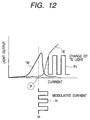
- the essence of this method is as follows. As shown in Fig. 12, a semiconductor laser with characteristics in which an input TM mode is converted into an output TE mode at a given current value is used.
- a specific current value at which TE and TM modes oscillate simultaneously is defined as a bias point, the threshold value gain of the TE and TM modes is switched by a signal current (modulated current) I S , and only light polarized in a specific direction is output onto a transmission path using a polarizer.
- the polarized wave modulation method has the following essential advantage. That is, since the optical density of a semiconductor laser is constant even during modulation (since the driving current is always nearly constant and is not turned on/off), carrier drifts caused by modulation can be minimized. However, the above-mentioned prior arts do not describe any detailed structures of such laser.
- a laser that can switch the polarized wave of output light is also disclosed in Japanese Patent Application Laid-Open No. 2-159781.
- the present invention proposes an optical device with a novel arrangement. Especially, the present invention proposes an optical device suitable for modulating the output intensity of light of a given polarized wave.
- One of optical devices according the present invention is as follows.
- An optical device comprises:
- a first oscillation state based on resonance mainly by the first resonator structure, and a second oscillation state based on resonance mainly by the second resonator structure can be switched. More specifically, by switching the degrees of contribution of the first and second resonator structures to oscillation in the compound resonator structure, the resonator structure, the resonance of which mainly contributes to oscillation can be selected.
- the oscillation state can be switched to a state (second oscillation state) wherein the oscillation is produced mainly by the Fabry-Pérot resonance.
- the output intensity of light of a predetermined polarized wave in the first oscillation state is set to be different from that of light of the predetermined polarized wave in the second oscillation state.
- the intensity of light can be switched by selecting whether this optical device is set in the first or second oscillation state.
- the intensity of the output light can be largely changed for one polarized wave. More specifically, for example, TM light is mainly output in one of the first and second oscillation states, and TE light is mainly output in the other state.
- the first and second oscillation states have different output intensities for the light of the predetermined polarized wave.
- strong oscillation e.g., a DFB or DBR mode is excited in the first oscillation state
- weak oscillation e.g., a Fabry-Pérot mode or a mixed mode of a Fabry-Pérot mode and a DFB or DBR mode
- a first region including the first resonator structure and a second region including the second resonator structure may be serially formed or may at least partially overlap each other, or the optical device may have a structure or region for coupling the first and second regions.
- the optical device may comprise control means for switching an oscillation state between the first and second oscillation states, control means for applying electrical control for switching an oscillation state between the first and second oscillation states, an electrode for applying electrical control for switching an oscillation state between the first and second oscillation states, an electrode for switching an oscillation state between the first and second oscillation states by controlling a carrier density to be injected, or an electrode for switching an oscillation state between the first and second oscillation states by controlling an electric field to be applied.
- the optical device may comprise a phase adjusting region for adjusting a phase of light in the optical device. By adjusting the phase, the first and second oscillation states can be switched.
- the optical device may comprise a phase adjusting region for adjusting a phase of light in the optical device independently of a first region including the first resonator structure and a second region including the second resonator structure.
- the optical device of the present invention can be formed by stacking semiconductor layers.
- the diffraction grating may be formed on an interface between two semiconductor layers.
- the diffraction grating may be formed on an interface between two semiconductor layers, and the optical device may further comprise means for adjusting a refractive index of at least one of the two semiconductor layers; the diffraction grating may be formed on an interface between two semiconductor layers, and at least one of the two semiconductor layers may include a quantum well structure; the diffraction grating may be formed on an interface between two semiconductor layers, and the optical device may further comprise control means for applying electrical control for adjusting a refractive index of at least one of the two semiconductor layers; the diffraction grating may be formed on an interface between two semiconductor layers, and the optical device may further comprise an electrode for applying electrical control for adjusting a refractive index of at least one of the two semiconductor layers; or the diffraction grating may be formed on an interface between two semiconductor layers, and the optical device may further comprise an electrode for applying an electrical field for adjusting a refractive index of at least one of the two semiconductor layers.
- the optical device may comprise a gain medium for producing a gain in the optical device.
- the optical device of the present invention need only be formed by stacking semiconductor layers, and in order to produce gain, an active layer containing a gain medium need only be formed.
- the optical device may comprise an active layer including a gain medium for producing a gain in the optical device, the active layer including a quantum well structure, and the active layer may include a plurality of quantum well structures.
- the plurality of quantum well structures may be at least partially different from each other to build an asymmetric quantum well structure.
- a strain stress may be applied on at least one of layers that build the quantum well structure.
- the strain stress is mainly determined by the lattice constants of the individual layers. By applying the strain stress, a desired gain spectrum can be efficiently obtained.
- the optical device may comprise a gain medium for producing a gain in the optical device, and a Bragg wavelength of the diffraction grating may be set in the vicinity of peak energy of the gain medium.
- the optical device may comprise an electrode for independently injecting carriers into a first region including the first resonator structure and a second region including the second resonator structure.
- An axial mode spacing of the Fabry-Pérot resonance may be set to be sufficiently smaller than a stop band based on the resonance by the diffraction grating in a region including the diffraction grating.
- the optical device may comprise means for controlling a degree of optical coupling between the first and second resonator structures, or a region for controlling a degree of optical coupling between the first and second resonator structures.
- the diffraction grating may have a phase discontinuous portion.
- the optical device may comprise a region where the diffraction grating is not formed.
- the region where no diffraction grating is formed is arranged to prevent the degree of resonance by the diffraction grating from excessively increasing in advance.
- One of optical devices of the present invention is as follows.
- An optical device comprises:
- One of optical devices of the present invention is as follows.
- An optical device comprises:
- One of optical devices of the present invention is as follows.
- An optical device comprises:
- the coupling coefficient of the diffraction grating can be controlled by the control means.
- the coupling coefficient is sufficiently large, oscillation is due mainly to resonance by the diffraction grating; when the coupling coefficient becomes small, oscillation is supported by Fabry-Pérot resonance between the two end faces of this optical device.
- One of optical devices of the present invention is as follows.
- An optical device comprises:
- An optical device comprises:
- An optical transmitter can be constituted using each of the above-mentioned optical devices.
- a polarized wave selector for extracting the light of the predetermined polarized wave from the output light of the optical device is preferably formed.
- a polarizer can be used as the polarized wave selector.
- this optical transmitter by switching the first and second oscillation states, the intensity of light extracted by the polarized wave selector is switched. Hence, by switching the first and second oscillation states in correspondence with the signal to be transmitted, an intensity-modulated optical signal can be obtained.
- a network for transmitting an optical signal can be built using the optical transmitter.
- One of methods of driving an optical device according to the present invention is as follows.
- a method of driving an optical device having a diffraction grating and at least two surfaces for reflecting light comprises the step of:
- switching between the first and second oscillation states may be attained by adjusting a phase of light in the optical device. For example, when the phase is controlled so that the phase of light oscillated in the first oscillation state becomes closer to a state that satisfies a resonance condition, the first oscillation state is obtained; when the phase of light in the optical device is changed to a state wherein the phase of light oscillated in the first oscillation state is separated away from the state that satisfies the resonance condition, and light to be oscillated in the second oscillation state oscillates more easily, the second oscillation state is obtained.
- switching between the first and second oscillation states may be attained by controlling a coupling coefficient of the diffraction grating.
- a light source that can be polarized-wave modulated need not set both TM and TE modes of oscillated light in a low chirp state, but can use one of these modes as a signal.
- each of the following embodiments aims at improving controllability and reliability of switching at the cost of coherence (single axial mode characteristics) of one mode.
- the basic arrangement in the first to fourth embodiments is as follows.
- equation (2) is a very important conditional formula that determines the oscillation mode (wavelength, polarized wave mode, transverse mode).
- the oscillation wavelength is discrete relative to the gain spectrum between the TE and TM modes as oscillation modes, it is hard to satisfy equations (2) and (3) at the same time.
- the reflectance and its loss spectrum viewed from an arbitrary one point in the resonator can be greatly changed by the coupling parameters (the coupling coefficient and phase between waveguides) of the resonator. Furthermore, by using the resonator distribution and polarized wave dependence of the gain, the threshold gains of TE and TM modes at the Bragg wavelength can be made nearly equal to each other.
- a phase adjusting region When a phase adjusting region is formed to modulate the phase, a situation in which the threshold value of, e.g., TM polarized light with respect to the DFB mode is lowered by feedback from another reflection end (e.g., the Fabry-Pérot resonator), and the DFB mode is stably oscillated as TM polarized light, and a situation in which the threshold value of the DFB mode as TE polarized light is raised by feedback from another reflection end (e.g., the DFB resonator), and the DFB and Fabry-Pérot modes (multimode) are oscillated as TE polarized light can be switched.
- the most characteristic portion of the present invention is that the phase matching condition between TE and TM can be satisfied more easily than the conventional arrangement.
- An asymmetric quantum well structure has a certain degree of freedom in varying the band gap and profile as compared to a symmetric quantum well structure. Furthermore, when a strain is asymmetrically introduced, the band gap can be selectively varied for the TE and TM modes. This means that the gain in a single active layer at a single injection carrier density can be set at the individual threshold gains of the TE and TM modes. The threshold carrier density is set at a modulation bias point, and a signal is superposed on an injection current or the injection current is phase-modulated to obtain a polarized wave-switched optical output.
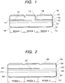
- Fig. 1 is a sectional view of the first embodiment of the present invention taken along the resonator direction.
- the detailed layer structure is as follows.
- an optical device has an n-InP substrate 101, an n-InP cladding layer 102, an n-InGaAsP light guide layer 103, an undoped GaInAsP active layer 104, a p-InP cladding layer 105, and a p-InGaAsP contact (capping) layer 106.
- the optical device has a grating 107 having a ⁇ /4 phase shift portion and formed between the n-cladding layer 102 and the n-light guide layer 103, a positive electrode 108, and a negative electrode 109.
- region 1 corresponds to a DFB region
- region 2 corresponds to a phase adjusting region
- region 3 corresponds to a Fabry-Pérot resonator (FP) region.
- a coupling parameter ⁇ L of the DFB region is about 2, and the resonator length of the FP region is set at 300 ⁇ m, thereby setting the axial mode spacing of the FP mode to be sufficiently smaller than the stop band.
- the individual regions are electrically independent from each other, but are optically coupled via the light guide layer 103 aligned in the resonator direction.
- the grating 107 is formed on the light guide layer 103, and its grating pitch is set so that the Bragg wavelength of the TM mode agrees with the gain peak.
- the two end faces form a Fabry-Pérot resonator.
- one end face uses a cleavage surface 112
- the other end face 110 uses an etching surface (etching mirror) 110.
- the depth of the etching surface 110 reaches the active layer 104 in this embodiment.
- the FP region can have both the functions of a reflecting mirror and an optical coupler.
- An end face 113 of the DFB region and the end face 112 of the FP region may be coated as needed.
- an anti-reflection (AR) coat 113 is formed on the DFB side, and a 50% reflecting coat 112 is formed the FP side.
- AR anti-reflection
- Figs. 3A and 3B show the gain spectra and resonator losses of the individual polarized waves (TE and TM) (the abscissa plots the wavelength, and the ordinate plots the gain or loss).
- the graphs in Figs. 3A and 3B overlap each other, and the oscillated mode has a resonator loss lower than the gain.
- the gain has an identical spectrum distribution (e.g., in the case of a bulk active layer) independently of the polarized light state for the sake of simplicity, whether or not the laser oscillates is determined by the resonator loss alone.
- a waveguide has different equivalent refractive indices with respect to TE polarized light and TM polarized light.
- the equivalent refractive index with respect to TE polarized light takes on a value about 0.2% larger than that with respect to TM polarized light.
- the threshold value changes depending on the phase of reflected light. For example, if the phase of the reflected light is different by a half wavelength from that of exit light, these light components cancel each other if they have an equal intensity, and exhibit an effect of increasing the threshold value. On the other hand, if these light components are in phase, they resonate, and decrease the threshold value.
- the threshold value of the DFB mode can be changed by light returning from another reflecting end (e.g., a Fabry-Pérot resonator).
- region 3 that builds the Fabry-Pérot laser amplifies the DFB mode and consumes the gain when light from the distributed feedback semiconductor laser is intense, oscillation is suppressed.
- the DFB mode becomes weak, the gain consumption amount in region 3 decreases to increase the gain of the Fabry-Pérot mode. In this case, if light is sufficiently excited, oscillation of the FP mode starts.
- the polarized light mode oscillated by the distributed feedback semiconductor laser is switched (e.g., polarized light is switched from TM polarized light to TE polarized light).
- the resonator mode can be switched between the DFB mode as TM polarized light and the mixed mode of the FP and DFB modes as TE polarized light.
- the resonator mode can be switched between a stable TM mode and a TE multimode. Whether the entire LD oscillates in the TE mode or TM mode is determined by the phase condition. In the phase adjusting region, the effective refractive index is changed by a plasma effect by injecting carriers.
- Fig. 4 shows the current (I) vs. light output (L) characteristics when a very weak signal current is superposed using the carrier injection amount as a modulation bias.
- the TE and TM modes can be switched by a small change in current, thus providing a great practical advantage.
- the total light output remains unchanged during modulation, and the influence of chirping is hardly observed.
- both TE and TM modes are single axial modes. Upon high-speed modulation, the TE mode becomes a multimode, but in the TM mode, a single axial mode maintains low chirp.
- a polarizer is inserted in front of the exit end face to select TM light alone, a low-chirp optical signal can be output.
- the DFB mode as the TM mode and FP/DFB multimode as the TE mode have been exemplified, but the converse is also true.
- a region where the reflectance of TM light is higher than that of TE light can be formed in a slab waveguide.
- the grating pitch is set, so that the Bragg wavelength of the TE mode agrees with the gain peak.
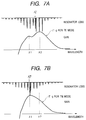
- Fig. 2 shows an optical device that can achieve the same operation and effect as those of the first embodiment by a different arrangement.
- region 1 corresponds to a gain region
- region 2 corresponds to a DFB region
- region 3 corresponds to a phase adjusting region.
- End faces 212 and 213 form a Fabry-Pérot resonator
- a grating 207 forms a second resonator.
- the optical device has an n-InP substrate 201, an n-InP cladding layer 202, an n-InGaAsP light guide layer 203, an undoped GaInAsP active layer 204, a p-InP cladding layer 205, and a p-InGaAsP contact layer 206.
- the optical device has a grating 207 having a ⁇ /4 phase shift portion and formed at the boundary between the n-cladding layer 202 and the n-light guide layer 203, a positive electrode 208, and a negative electrode 209.
- a means for coupling a plurality of waveguides is realized by forming a common light guide layer.
- the operation principle of the device is substantially the same as that described above with the aid of Figs. 3A, 3B and 4 in the first embodiment.
- the characteristics can be further improved by controlling the profile of a gain g in conditional formulas (2) and (3).
- An embodiment that exploits the polarized wave dependence of the gain will be explained below.
- Fig. 5 shows the band structure of the active layer.
- the peak wavelengths of photoluminescences of quantum well 1 and quantum well 2 (a quantum well lay on the low energy side, which contributes to the gain of TE modes) are respectively set at 1.550 ⁇ m and 1.5 ⁇ m.
- a strain of 2.0% tensile strain is introduced into quantum well 1 alone (which is a quantum well layer on the high energy side, and contributes to the gain of TM modes).
- the active layer 104 or 204 in the first or second embodiment is replaced by an active layer with this band structure.
- the grating pitch of the DFB region is set so that at least one of the Bragg wavelengths of two guided mode is set in the vicinity of the gain spectrum peak wavelength of the asymmetrical quantum well.
- Fig. 6 shows the gain spectrum of ⁇ g at a certain carrier density (injection current).
- the threshold carrier density threshold gain
- modulation efficiency is improved (polarized wave modulation can be achieved with a smaller change in current or voltage or the like, since the effective mass becomes small, and carriers become easier to move)
- the polarized wave dependence of the gain spectrum can be increased and the gain peak wavelength of TE and TM modes can be varied, and so on.
- Figs. 7A and 7B show the relationship between the ⁇ g (gain ⁇ confinement coefficient) and the resonator loss viewed from an arbitrary one point in a state wherein carriers are injected in the vicinity of the threshold value of this embodiment in correspondence with TE and TM modes.
- This embodiment has a merit of optimizing the gain profiles of TM and TE modes.
- the operation principle is substantially the same as that described above with the aid of Figs. 3A, 3B and 4 in the first embodiment.
- a tensile strain is introduced into only the quantum well on the high energy side.
- a compression strain may be introduced into only the quantum well on the low energy side, or a tensile strain and a compression strain may be respectively introduced into high- and low-energy quantum wells. Since a two-layered quantum well may pose a problem of saturation of the gain, an asymmetric stacked strained quantum well layer may be formed by stacking a plurality of active layers.
- variable dividing ratio mechanism suitable for the present invention, mechanisms described in Japanese Patent Application Nos. 5-80170 and 5-352709 filed by the present applicant are known. In this embodiment, such variable dividing ratio mechanism is applied to the second embodiment.
- Fig. 8 is a sectional view of the optical device taken along the resonator direction
- Fig. 9 is a sectional view of the device taken along a direction perpendicular to the resonator direction. Since the dividing/multiplexing ratios can be controlled by coupler portions in regions 1 and 3, the control range of the resonator loss spectrum can be broadened. That is, the polarized wave modulation range can be broadened (the current, applied voltage, and the like of each region need be adjusted as a preprocess of polarized wave modulation, but the adjustment range can be broadened).
- the optical device shown in Fig. 8 comprises an n-GaAs substrate 300, an n-AlGaAs first cladding layer 301, an n-AlGaAs first core layer 302, a p-AlGaAs second cladding layer 303, an undoped AlGaAs second core layer 304, an n-AlGaAs third cladding layer 305, and a contact layer (GaAs) 306.
- the optical device comprises a positive electrode 307a, negative electrode 307b and 308, and a periodic current confinement layer 309 for modulating the refractive index. Reflection coats 311 are formed on the end faces.
- a first cladding layer 301 to the lower layer of a second cladding layer 303 are grown on an n-GaAs substrate 300.
- MOCVD metal organic chemical vapor deposition
- MBE molecular beam epitaxial growth
- a first cladding layer 301 to the lower layer of a second cladding layer 303 are grown on an n-GaAs substrate 300.
- an n-AlGaAs layer is formed, and a grating pattern with an appropriate pitch is formed by etching so that its depth reaches a p-AlGaAs layer (the lower layer of the second cladding layer 303).
- MOCVD metal organic chemical vapor deposition
- MBE molecular beam epitaxial growth
- a periodic current confinement layer 309 is formed.
- an undoped AlGaAs second core layer 304 and the lower layer of a third cladding layer 305 are grown, and a grating 310 in region 4 is formed.
- the upper layer of the third cladding layer 305 and a contact layer 306 are grown.
- a buried structure or the like is formed, and electrodes 307a, 307b, and 308 are formed, thus completing the structure of this embodiment.
- the optical device has a p-AlGaAs buried layer 320, an n-buried layer 321, and a current path 330 between the positive and negative electrodes 307a and 307b.
- the carrier distribution is modulated by the periodic current confinement layer 309 to form a carrier distribution in the first core layer 302, thus forming an equivalent refractive index distribution corresponding to the carrier distribution.
- the first and second core layers 302 and 304 are coupled by the periodic current confinement layer 309.
- the degree of coupling can be controlled by the carrier injection state into regions 1 and 3. This corresponds to the control of the coupling coefficient between the waveguide of a DFB resonator region and that of a Fabry-Pérot resonator region.
- TE and TM modes can be selectively oscillated by the same operation principle as in the above embodiment.
- An optical coupler portion may be formed in one region.
- phase adjusting control, and coupling control between the DFB region and the Fabry-Pérot region are made.
- Figs. 3A and 3B show the relationship between the ⁇ g (gain ⁇ confinement coefficient) spectrum and the resonator loss spectrum viewed from an arbitrary one point in a state wherein carriers are injected and excited in the vicinity of the threshold value of this embodiment in correspondence with TE and TM modes.
- the active layer 104 uses a bulk structure without any quantum effect
- the TE and TM modes have nearly no difference between their values of ⁇ g (gain ⁇ confinement coefficient) profiles although they have a difference between their confinement coefficients ⁇ .
- the resonator loss as the TE mode, since the axial mode suppression ratio becomes small, some axial modes that can oscillate are always present (see Fig. 3B) in cooperation with the broad gain spectrum of the TE mode.
- the TM mode since the axial mode suppression ratio becomes large, a Bragg wavelength ⁇ TM B can always be selected as an oscillation mode (Fig. 3A).
- the oscillation mode can be switched between a stable TM mode and a TE multimode. Whether the entire LD oscillates in the TE mode or TM mode is determined by the phase condition. In the phase adjusting region, the effective refractive index is changed by a plasma effect by injecting carriers.
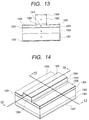
- Fig. 13 best illustrates the characteristic feature of this embodiment as a distributed feedback semiconductor laser and shows a section taken along a line 13 - 13 (a direction perpendicular to the resonance direction) in Fig. 14.
- the device comprises an n-InP substrate 1301, an n-InP first cladding layer 1302, an active layer 1303 made up of a quantum well, a p-InGaAsP first light guide layer 1304, a diffraction grating 1305, a second light guide layer 1310 made up of, e.g., a quantum well, an n-InP second cladding layer 1306, a first electrode 1307 formed on the substrate 1301, a second electrode 1308 formed on a portion on the first light guide layer 1304, and a third electrode 1309 formed on the second cladding layer 1306.
- Fig. 15 is a sectional view taken along a line 15 - 15 (the resonance direction) in Fig. 14.
- the two end faces are cleavage surfaces and build a Fabry-Pérot resonator.
- Figs. 13, 14, and 15 the same reference numerals denote the same members.
- the device of this embodiment adopts a ridge waveguide, which has a width of about 3 ⁇ m and an element length of about 500 ⁇ m.
- the diffraction grating 1305 is formed to have a period of 230 nm and a depth of about 30 nm.
- the Bragg wavelength of the diffraction grating 1305 with respect to a TE polarized wave is set at the gain peak wavelength in cooperation with the arrangement of the active layer 1303.
- no heavily doped layer for improving contacts is illustrated between the second electrode 1308 and the first light guide layer 1304, but such heavily doped layer is used for decreasing the contact resistance.
- the active layer 1303 has a so-called tensilely strained quantum well structure using a material (InGaAsP) with a smaller lattice constant than that of the substrate 1301, and in the quantum level formed in the valence band, the level of light holes is the lowest-order level.
- a material InGaAsP
- the gain for a TM polarized wave is set to be larger than that for a TE polarized wave.
- the second light guide layer 1310 has a quantum well structure that does not serve as an absorption layer with respect to light produced by the active layer 1303, and its refractive index changes (increases) by applying a reverse bias.
- the reverse bias is applied to the second light guide layer 1310 via the second and third electrodes 1308 and 1309.
- the second electrode 1308 serves as a common electrode, i.e., operates while being grounded.
- Current injection into the active layer 1303 is performed by applying a forward bias voltage using the first and second electrodes 1307 and 1308.
- a reverse bias voltage is applied to the second light guide layer 1310 that forms the diffraction grating 1305 using the second and third electrodes 1308 and 1309 to cause a quantum confinement Stark effect in the quantum wells that build the second light guide layer 1310, thereby changing the refractive index.
- the refractive index increases slightly, and the refractive index difference between the materials that sandwich the diffraction grating 1305 therebetween, i.e., between the first and second light guide layers 1304 and 1310 decreases.
- the coupling coefficient of the diffraction grating 1305 decreases.
- the decrease in coupling coefficient stops the oscillation in the DFB mode that has taken place before voltage application, and causes switching to an FP mode oscillation that resonates between the two end faces.
- the FP mode oscillation becomes TM polarized wave oscillation since the active layer 1303 has the tensilely strained quantum well structure.
- the coupling coefficient of the diffraction grating 1305 can be increased, and the oscillation mode can be switched from the FP mode to the DFB mode again.
- the DFB mode and FP mode correspond to TE polarized wave oscillation or TM polarized wave oscillation can be appropriately set in design of the arrangement of the active layer, the pitch of the diffraction grating, and the like.
- a voltage is applied to the diffraction grating 1303, which has ⁇ L (the product of the coupling coefficient of the diffraction grating 1305 and the resonator length) of about 1.2 (about 70% as a reflectance), while no reverse bias is applied to the diffraction grating 1305, so as to decrease the refractive index difference between the first and second light guide layers 1304 and 1310, thereby halving ⁇ L.
- ⁇ L the product of the coupling coefficient of the diffraction grating 1305 and the resonator length
- a tensilely strained quantum well structure is used as the active layer in which TE and TM polarized waves have nearly equal gains.
- the present invention is not limited to this, and an active layer having a bulk structure may be used.
- the means for changing the refractive index of the guide layer is not limited to voltage application, but may use a plasma effect by current injection, and the like.
- a forward bias voltage may be applied to the second light guide layer 1310 using the second and third electrodes 1308 and 1309 to attain current injection.
- a phase discontinuous portion (e.g., a ⁇ /4 phase shift portion 1315) is preferably formed in the diffraction grating 1305 to stabilize the DFB mode (such means is the same as that in a conventional DFB laser; Fig. 16 shows the sectional arrangement in the resonance direction).
- three electrodes 1320, 1321, and 1322 are formed, and are used for current control for varying the wavelength, adjusting the phase, and so on.
- This embodiment adopts the DFB laser arrangement, but may adopt a DBR laser arrangement in which an active region which has the active layer 1303 and a flat light guide layer and has no diffraction grating 1305, and a DBR region which has an electrode 1309 for applying a voltage to the diffraction grating 1305 between the first and second light guide layers 1304 and 1310, and the second light guide layer 1310, are formed in series in the resonance direction.
- the operation of the DBR laser is substantially the same as that of the above-mentioned DFB laser.
- current injection into the active layer 1303 in the active region is attained by applying a forward bias voltage using the first and second electrodes 1307 and 1308, while a reverse bias voltage is applied to the second light guide layer 1310 that forms the diffraction grating 1305 in the DBR region using the second and third electrodes 1308 and 1309 to cause the quantum confinement Stark effect, thereby changing the refractive index.
- Fig. 17 shows the sixth embodiment of the present invention.
- Fig. 17 corresponds to Fig. 15 of the fifth embodiment.
- the same reference numerals in Fig. 17 denote the same parts as in the fifth embodiment.
- the section perpendicular to the resonance direction is the same as that shown in Fig. 13 in a region with the diffraction grating 1305.
- the difference between the sixth and fifth embodiments is that a portion where no diffraction grating is formed is present on the right side in Fig. 17. If the depth of the diffraction grating 1305 is set to be the same as that in the fifth embodiment, and also the element length remains the same, the parameter ⁇ L that influences reflections by the diffraction grating decreases. In the sixth embodiment, the length of a portion where the diffraction grating 1305 is formed is reduced to about 80% of the fifth embodiment. With this structure, although the threshold value for an oscillation in the DFB mode is raised slightly, the coupling coefficient of the diffraction grating 1305 need only be decreased by a smaller amount upon switching to the FP mode.
- the voltages to be applied across the electrodes 1308 and 1309, and electrodes 1307 and 1323 can be lowered upon switching to the FP mode.
- currents injection currents into the active layer 1303 across the electrodes 1307 and 1308 are preferably increased.
- Fig. 18 corresponds to Fig. 13 of the fifth embodiment.
- the same reference numerals in Fig. 18 denote the same parts as in Fig. 13.
- a new member in Fig. 18 is a current confinement layer 1340.
- Fig. 19 shows an embodiment when the element described in each of the first to seventh embodiments is used in an optical transmitter.
- Fig. 19 illustrates an optical transmitter 1330, a control circuit 1331, a device 1332 according to the present invention, a polarization selecting means (e.g., a polarizer) 1333, a signal 1334 to be transmitted, an optical signal 1335 output from the optical transmitter 1330, a signal 1336 which is output from the control circuit 1331 to control driving of the device 1332 of the present invention, and a light output 1337 output from the device 1332 of the present invention.
- a polarization selecting means e.g., a polarizer
- the optical transmitter 1330 that received a signal 1334 to be transmitted from an external device generates a control drive signal 1336 for driving the device 1332 of the present invention on the basis of the principle described so far in the above embodiments.
- the device 1332 of the present invention switches the light output state between a DFB mode as a TE polarized wave (or a DFB mode as a TM polarized wave) and an FP mode as a TM polarized wave (or a FP mode as a TE polarized wave).
- the obtained light output 1337 is input to the polarization selecting means 1333 to select a light output of one polarization state (e.g., light of the DFB mode as the TE polarized wave), thus obtaining an optical signal 1335 corresponding to the signal 1334.
- a light output of one polarization state e.g., light of the DFB mode as the TE polarized wave
- the mode of light can be appropriately selected in correspondence with situations.
- Fig. 20 shows the arrangement of an opto-electric conversion unit (node) connected to terminal equipments when a semiconductor device according to the present invention is applied to a wavelength multiplexing optical LAN system
- Figs. 10 and 11 show the arrangements of optical LAN systems using such node 701.
- An optical signal transmitted via an optical fiber 700 as a medium connected to an external device is received by a node 701, and some signal components are input to a receiver 703 comprising, e.g., a variable wavelength optical filter, and the like via a divider 702.
- the receiver 703 extracts only an optical signal of a desired wavelength and performs signal detection.
- the detected signal is processed by a control circuit by an appropriate method, and the processed signal is sent to a terminal equipment.
- a polarized wave modulation semiconductor laser 704 of each of the above embodiments is driven by a control circuit in accordance with an appropriate method, as described above, to polarized wave-modulate the optical signal.
- the modulated optical signal is input to a polarizer 707 (to convert the polarized wave-modulated signal into an amplitude/intensity-modulated signal), and output light is transmitted onto an optical transmission path via a power multiplexer 706 (an isolator may be further inserted).
- a plurality of sets of semiconductor lasers and variable wavelength optical filters may be arranged to broaden the variable wavelength range.
- the optical LAN system shown in Fig. 10 adopts a bus type network, in which nodes 801 to 805 are connected in directions A and B, and a large number of terminal equipments and centers 811 to 815 can be connected via the network.
- light amplifiers In order to connect a large number of nodes, light amplifiers must be serially arranged on a transmission path 800 to compensate for attenuation of light.
- Two out of the nodes 801 to 805 may be connected to each of the terminal equipments 811 to 815 to form two transmission paths, thus allowing two-way transmissions based on a DQDB scheme.
- a loop type that connects A and B in Fig. 10 shown in Fig. 11
- a star type a combination of these types, and the like are available.
- the system shown in Fig. 11 includes an optical transmission path 900, optical nodes 901 to 906, and terminal equipments 911 to 914.
- the oscillation state is switched between a first oscillation state mainly based on resonance by distributed reflection by the diffraction grating, and a second oscillation state mainly based on Fabry-Pérot resonance between the two surfaces.
- the characteristics of one of two modes to be used are improved at the cost of coherence of the other mode.
Landscapes
- Physics & Mathematics (AREA)
- Optics & Photonics (AREA)
- Condensed Matter Physics & Semiconductors (AREA)
- General Physics & Mathematics (AREA)
- Electromagnetism (AREA)
- Engineering & Computer Science (AREA)
- Nanotechnology (AREA)
- Chemical & Material Sciences (AREA)
- Biophysics (AREA)
- Crystallography & Structural Chemistry (AREA)
- Life Sciences & Earth Sciences (AREA)
- Semiconductor Lasers (AREA)
- Optical Communication System (AREA)
- Mechanical Light Control Or Optical Switches (AREA)
Applications Claiming Priority (9)
| Application Number | Priority Date | Filing Date | Title |
|---|---|---|---|
| JP23980196 | 1996-08-22 | ||
| JP23980196 | 1996-08-22 | ||
| JP239801/96 | 1996-08-22 | ||
| JP26030796A JP3382471B2 (ja) | 1995-09-18 | 1996-09-09 | 半導体光デバイス及びそれを用いた光ネットワーク |
| JP260307/96 | 1996-09-09 | ||
| JP26030796 | 1996-09-09 | ||
| JP22307997 | 1997-08-05 | ||
| JP223079/97 | 1997-08-05 | ||
| JP9223079A JPH10117046A (ja) | 1996-08-22 | 1997-08-05 | 半導体レーザ及びその駆動法及びそれを用いた光送信器及びそれを用いた光通信システム |
Publications (2)
| Publication Number | Publication Date |
|---|---|
| EP0825689A2 true EP0825689A2 (fr) | 1998-02-25 |
| EP0825689A3 EP0825689A3 (fr) | 2001-05-09 |
Family
ID=27330738
Family Applications (1)
| Application Number | Title | Priority Date | Filing Date |
|---|---|---|---|
| EP97114493A Withdrawn EP0825689A3 (fr) | 1996-08-22 | 1997-08-21 | Dispositif optique à l'émission de lumière polarisée commutable, transmetteur optique utilisant ce dispositif, et méthode de commutation d'un dispositif optique |
Country Status (2)
| Country | Link |
|---|---|
| US (1) | US6031860A (fr) |
| EP (1) | EP0825689A3 (fr) |
Cited By (2)
| Publication number | Priority date | Publication date | Assignee | Title |
|---|---|---|---|---|
| WO2003009434A3 (fr) * | 2001-07-14 | 2003-08-28 | Bookham Technology | Laser accordable |
| WO2004098005A1 (fr) | 2003-04-30 | 2004-11-11 | Nanoplus Nanosystems And Technologies Gmbh | Laser multisection |
Families Citing this family (27)
| Publication number | Priority date | Publication date | Assignee | Title |
|---|---|---|---|---|
| JP2002043698A (ja) * | 1999-12-22 | 2002-02-08 | Yokogawa Electric Corp | Shgレーザ光源及びshgレーザ光源の変調方法 |
| JP2002094176A (ja) * | 2000-09-14 | 2002-03-29 | Mitsubishi Electric Corp | レーザ装置 |
| JP2002141604A (ja) * | 2000-11-07 | 2002-05-17 | Sony Corp | 半導体レーザ |
| FR2821495B1 (fr) * | 2001-02-23 | 2004-08-27 | Cit Alcatel | Laser accordable de facon rapide et large |
| US6628686B1 (en) * | 2001-11-16 | 2003-09-30 | Fox-Tek, Inc | Integrated multi-wavelength and wideband lasers |
| US7369863B2 (en) * | 2001-11-30 | 2008-05-06 | Siemens Aktiengesellschaft | Positional data recording |
| US6638773B1 (en) * | 2002-05-31 | 2003-10-28 | Applied Optoelectronics, Inc. | Method for fabricating single-mode DBR laser with improved yield |
| KR100519922B1 (ko) * | 2002-12-17 | 2005-10-10 | 한국전자통신연구원 | 다영역 자기모드 잠김 반도체 레이저 다이오드 |
| US7573928B1 (en) * | 2003-09-05 | 2009-08-11 | Santur Corporation | Semiconductor distributed feedback (DFB) laser array with integrated attenuator |
| WO2006008873A1 (fr) * | 2004-07-15 | 2006-01-26 | Nec Corporation | Laser de longueur variable à résonateur externe |
| US7436871B2 (en) * | 2004-12-03 | 2008-10-14 | Corning Incorporated | Method and device for performing wavelength modulation with Distributed Bragg Reflector (DBR) laser |
| US7483466B2 (en) * | 2005-04-28 | 2009-01-27 | Canon Kabushiki Kaisha | Vertical cavity surface emitting laser device |
| US7583725B1 (en) * | 2005-06-22 | 2009-09-01 | Xilinx, Inc. | Dynamically reconfigurable adaptive communication device and system |
| KR100753816B1 (ko) * | 2005-10-25 | 2007-08-31 | 한국전자통신연구원 | 수동 모드 잠김을 일으키는 레이저 다이오드 및 그 다이오드를 이용한 광 펄스 생성 방법 |
| KR100776099B1 (ko) | 2006-03-06 | 2007-11-15 | 엘에스전선 주식회사 | 듀얼 타입 레이저 다이오드 및 그 제조방법 |
| FR2906412B1 (fr) * | 2006-09-22 | 2008-11-14 | Alcatel Sa | Laser accordable a reseau de bragg distribue comportant une section de bragg en materiau massif contraint |
| FR2909491B1 (fr) * | 2006-12-05 | 2010-04-23 | Commissariat Energie Atomique | Dispositif laser a source laser et guide d'onde couples |
| US7567595B2 (en) * | 2007-10-01 | 2009-07-28 | Corning Incorporated | Laser source with interdigital heater electrodes and underlying current confinement layer |
| US7715453B2 (en) * | 2007-11-20 | 2010-05-11 | Corning Incorporated | Wavelength control in phase region of semiconductor lasers |
| WO2010073392A1 (fr) * | 2008-12-26 | 2010-07-01 | 富士通株式会社 | Dispositif de génération de signal optique et son procédé d'ajustement |
| US20110134957A1 (en) * | 2009-12-07 | 2011-06-09 | Emcore Corporation | Low Chirp Coherent Light Source |
| JP5597029B2 (ja) * | 2010-05-27 | 2014-10-01 | 住友電気工業株式会社 | 波長可変半導体レーザ |
| US9306672B2 (en) | 2013-03-14 | 2016-04-05 | Encore Corporation | Method of fabricating and operating an optical modulator |
| US9059801B1 (en) | 2013-03-14 | 2015-06-16 | Emcore Corporation | Optical modulator |
| US9306372B2 (en) | 2013-03-14 | 2016-04-05 | Emcore Corporation | Method of fabricating and operating an optical modulator |
| US9564733B2 (en) | 2014-09-15 | 2017-02-07 | Emcore Corporation | Method of fabricating and operating an optical modulator |
| US10074959B2 (en) | 2016-08-03 | 2018-09-11 | Emcore Corporation | Modulated laser source and methods of its fabrication and operation |
Family Cites Families (19)
| Publication number | Priority date | Publication date | Assignee | Title |
|---|---|---|---|---|
| JPS58196088A (ja) * | 1982-05-12 | 1983-11-15 | Hitachi Ltd | 半導体レ−ザ素子 |
| JPS6242593A (ja) * | 1985-08-20 | 1987-02-24 | Fujitsu Ltd | 半導体発光装置 |
| JPS62144426A (ja) * | 1985-12-19 | 1987-06-27 | Matsushita Electric Ind Co Ltd | 光伝送装置 |
| JPS63299291A (ja) * | 1987-05-29 | 1988-12-06 | Kokusai Denshin Denwa Co Ltd <Kdd> | 半導体レ−ザ |
| FR2639773B1 (fr) * | 1988-11-25 | 1994-05-13 | Alcatel Nv | Laser a semi-conducteur accordable |
| JPH02159781A (ja) * | 1988-12-14 | 1990-06-19 | Toshiba Corp | 光通信装置 |
| US5202782A (en) * | 1990-01-19 | 1993-04-13 | Canon Kabushiki Kaisha | Optical communication method and optical communication system |
| JP3104798B2 (ja) * | 1991-03-12 | 2000-10-30 | キヤノン株式会社 | 集積型光カップラ及びその製造方法 |
| JP2986604B2 (ja) * | 1992-01-13 | 1999-12-06 | キヤノン株式会社 | 半導体光フィルタ、その選択波長の制御方法及びそれを用いた光通信システム |
| EP0562518B1 (fr) * | 1992-03-23 | 1997-12-29 | Canon Kabushiki Kaisha | Dispositif optique et méthode utilisant ce dispositif utilisant l'apparition d'une variation de tension entre les deux bornes d'une région amplificatrice |
| JPH0661571A (ja) * | 1992-08-05 | 1994-03-04 | Nippon Telegr & Teleph Corp <Ntt> | 分布光反射器及びそれを用いた半導体レーザ |
| JP3302088B2 (ja) * | 1993-03-15 | 2002-07-15 | キヤノン株式会社 | 集積型光デバイスおよびそれを用いた光通信ネットワーク |
| JP3104831B2 (ja) * | 1993-12-29 | 2000-10-30 | キヤノン株式会社 | 集積型光デバイス及びそれを用いた光通信ネットワーク |
| EP0620475B1 (fr) * | 1993-03-15 | 1998-12-30 | Canon Kabushiki Kaisha | Dispositifs optiques et systèmes de communication optique qui les utilisent |
| EP0668641B1 (fr) * | 1994-02-18 | 2001-06-06 | Canon Kabushiki Kaisha | Laser à semi-conducteur avec sélectivité du mode de polarisation, transmetteur de lumière et système optique de communication utilisant ce laser |
| JP3263553B2 (ja) * | 1994-02-23 | 2002-03-04 | キヤノン株式会社 | 光送信機 |
| JPH07307530A (ja) * | 1994-03-17 | 1995-11-21 | Canon Inc | 偏波変調可能な半導体レーザ |
| JP3303515B2 (ja) * | 1994-03-18 | 2002-07-22 | キヤノン株式会社 | 光通信方式及びそれを用いた光通信システム |
| US5648978A (en) * | 1995-01-04 | 1997-07-15 | Canon Kabushiki Kaisha | Oscillation polarization mode selective semiconductor laser, modulation method therefor and optical communication system using the same |
-
1997
- 1997-08-21 US US08/915,664 patent/US6031860A/en not_active Expired - Fee Related
- 1997-08-21 EP EP97114493A patent/EP0825689A3/fr not_active Withdrawn
Cited By (3)
| Publication number | Priority date | Publication date | Assignee | Title |
|---|---|---|---|---|
| WO2003009434A3 (fr) * | 2001-07-14 | 2003-08-28 | Bookham Technology | Laser accordable |
| US7257137B2 (en) | 2001-07-14 | 2007-08-14 | Bookham Technology, Plc | Tuneable laser having comb reflectors producing combs of reflective wavelength peaks |
| WO2004098005A1 (fr) | 2003-04-30 | 2004-11-11 | Nanoplus Nanosystems And Technologies Gmbh | Laser multisection |
Also Published As
| Publication number | Publication date |
|---|---|
| EP0825689A3 (fr) | 2001-05-09 |
| US6031860A (en) | 2000-02-29 |
Similar Documents
| Publication | Publication Date | Title |
|---|---|---|
| US6031860A (en) | Optical device capable of switching output intensity of light of predetermined polarized wave, optical transmitter using the device, network using the transmitter, and method of driving optical device | |
| EP0674372B1 (fr) | Laser à semi-conducteur sélectif à la polarisation de l'émission et système optique de communication utilisant ce laser | |
| US5757828A (en) | Semiconductor laser device, method for driving the same, and optical communication system using the same | |
| US5764670A (en) | Semiconductor laser apparatus requiring no external modulator, method of driving semiconductor laser device, and optical communication system using the semiconductor laser apparatus | |
| EP0721240B1 (fr) | Laser à semi-conducteur à sélectivité du mode de polarisation, méthode de modulation, et système de communication optique utilisant ce laser | |
| US6008675A (en) | Polarization-mode selective semiconductor laser with a bending channel stripe, apparatus including the same and optical communication system using the same | |
| EP0668641B1 (fr) | Laser à semi-conducteur avec sélectivité du mode de polarisation, transmetteur de lumière et système optique de communication utilisant ce laser | |
| US5841799A (en) | Semiconductor laser, modulation method therefor and optical communication system using the same | |
| US6252895B1 (en) | Distributed feedback semiconductor laser in which light intensity distributions differ in different polarization modes, and driving method therefor | |
| EP0735635B1 (fr) | Appareil optique semi-conducteur, sa méthode de commande, appareil source lumineuse et système de communication optique utilisant celui-ci | |
| US5757832A (en) | Optical semiconductor device, driving method therefor and light source and opitcal communication system using the same | |
| US5926497A (en) | Diffraction grating with alternately-arranged different regions, optical semiconductor device with the diffraction grating, and apparatus and optical communication system using the same | |
| EP0668642B1 (fr) | Laser à semi-conducteur avec selectivité du mode de polarisation, transmetteur de lumière et système optique de communication utilisant ce laser | |
| US6337868B1 (en) | Distributed feedback semiconductor laser and a driving method therefor | |
| EP0911927A1 (fr) | Source laser à semiconducteur accordable à bande large | |
| US5757840A (en) | Semiconductor laser modulation method therefor and optical communication system using the same | |
| Okai et al. | Complex-coupled/spl lambda//4-shifted DFB lasers with a flat FM response | |
| JP3246703B2 (ja) | 偏波変調可能な半導体レーザおよびこれを用いた光通信方式 | |
| Numai | 1.5 mu m two-section Fabry-Perot wavelength tunable optical filter | |
| JPH08172243A (ja) | 光伝送装置及びその変調方式 | |
| JP3303653B2 (ja) | 半導体レーザ装置、その駆動方法及びそれを用いた光通信システム | |
| JPH08172234A (ja) | 光伝送装置およびその変調方式 | |
| JP3387722B2 (ja) | 半導体レーザ装置及びそれを用いた光通信システム | |
| JPH0983087A (ja) | 偏波制御および波長制御可能な半導体光デバイスおよびそれを用いた光ネットワーク | |
| JPH10117046A (ja) | 半導体レーザ及びその駆動法及びそれを用いた光送信器及びそれを用いた光通信システム |
Legal Events
| Date | Code | Title | Description |
|---|---|---|---|
| PUAI | Public reference made under article 153(3) epc to a published international application that has entered the european phase |
Free format text: ORIGINAL CODE: 0009012 |
|
| AK | Designated contracting states |
Kind code of ref document: A2 Designated state(s): DE FR GB IT NL SE |
|
| AX | Request for extension of the european patent |
Free format text: AL;LT;LV;RO;SI |
|
| PUAL | Search report despatched |
Free format text: ORIGINAL CODE: 0009013 |
|
| AK | Designated contracting states |
Kind code of ref document: A3 Designated state(s): AT BE CH DE DK ES FI FR GB GR IE IT LI LU MC NL PT SE |
|
| AX | Request for extension of the european patent |
Free format text: AL;LT;LV;RO;SI |
|
| 17P | Request for examination filed |
Effective date: 20010921 |
|
| AKX | Designation fees paid |
Free format text: DE FR GB IT NL SE |
|
| 17Q | First examination report despatched |
Effective date: 20030507 |
|
| STAA | Information on the status of an ep patent application or granted ep patent |
Free format text: STATUS: THE APPLICATION HAS BEEN WITHDRAWN |
|
| 18W | Application withdrawn |
Effective date: 20090806 |