EP0825743A2 - Vorverzerrung für Mehrträgersender - Google Patents
Vorverzerrung für Mehrträgersender Download PDFInfo
- Publication number
- EP0825743A2 EP0825743A2 EP97306465A EP97306465A EP0825743A2 EP 0825743 A2 EP0825743 A2 EP 0825743A2 EP 97306465 A EP97306465 A EP 97306465A EP 97306465 A EP97306465 A EP 97306465A EP 0825743 A2 EP0825743 A2 EP 0825743A2
- Authority
- EP
- European Patent Office
- Prior art keywords
- signal
- correcting
- digital
- converting
- characteristic
- Prior art date
- Legal status (The legal status is an assumption and is not a legal conclusion. Google has not performed a legal analysis and makes no representation as to the accuracy of the status listed.)
- Ceased
Links
Images


Classifications
-
- H—ELECTRICITY
- H04—ELECTRIC COMMUNICATION TECHNIQUE
- H04L—TRANSMISSION OF DIGITAL INFORMATION, e.g. TELEGRAPHIC COMMUNICATION
- H04L27/00—Modulated-carrier systems
- H04L27/26—Systems using multi-frequency codes
- H04L27/2601—Multicarrier modulation systems
- H04L27/2626—Arrangements specific to the transmitter only
-
- H—ELECTRICITY
- H04—ELECTRIC COMMUNICATION TECHNIQUE
- H04L—TRANSMISSION OF DIGITAL INFORMATION, e.g. TELEGRAPHIC COMMUNICATION
- H04L27/00—Modulated-carrier systems
- H04L27/26—Systems using multi-frequency codes
- H04L27/2601—Multicarrier modulation systems
- H04L27/2647—Arrangements specific to the receiver only
- H04L27/2649—Demodulators
- H04L27/265—Fourier transform demodulators, e.g. fast Fourier transform [FFT] or discrete Fourier transform [DFT] demodulators
Definitions
- the present invention relates to a correction circuit and method suitable for modulation/demodulation processing in the case where communication using multi-carrier signals is conducted, and also relates to a receiving device and a transmitting device to which such a correction circuit and method may be applied.
- a communication system using a signal called a multi-carrier signal.
- a plurality of carriers are simultaneously transmitted, and information is distributed to each of the carriers to conduct communication, so that an efficient transmission becomes possible.
- OFDM orthogonal frequency division multiplex
- the present applicant proposed a transmission system using a signal having a configuration referred to as an orthogonal frequency division multiplex (OFDM) wave (as in Japanese laid-open patent publication No. 8-132434, and so on).
- OFDM orthogonal frequency division multiplex
- a time slot is formed by taking a predetermined time as a unit.
- band slots divided on the frequency axis are prescribed in the time slot. Processing of simultaneously transmitting a plurality of carrier signals located at a bandslot interval by using a predetermined number of band slots is conducted at a predetermined time slot period.
- FIG. 1 is a diagram showing an example of configuration of a conventional receiving circuit of this OFDM wave.
- a signal 106 fed from an antenna or an amplifier (neither of them is illustrated) undergoes frequency conversion in a down converter 102 to produce an intermediate frequency signal or a baseband signal.
- a frequency converted signal 107 is supplied to a low-pass filter 103, in which a carrier component and so on are removed to produce an OFDM wave 108 which is a multi-carrier signal.
- This OFDM wave 108 is a multi-carrier signal containing a signal in a certain carrier interval (i.e., the above described band slot interval).
- the OFDM wave 108 is converted to a digital signal in an analog/digital converter 104.
- Converted data are supplied to a fast Fourier transform circuit (hereafter referred to as FFT) 105.
- FFT fast Fourier transform circuit
- the FFT 105 conducts processing for converting an inputted signal 109 formed in a time sequence to a signal 110 on a frequency sequence.
- the signal 110 on the frequency sequence is selected by a signal selection circuit 101. Since oversampling of a doubled rate is now conducted in the analog/digital converter 104, processing of selecting information contained in half carriers of the output from of the FFT 105 is conducted.
- a selected signal 111 is used as a received symbol sequence.
- FIGS. 2A to 2E The state of the signal received by the circuit of FIG. 1 is shown in FIGS. 2A to 2E.
- FIG. 2A shows waveforms of values of a real part and an imaginary part, the amplitude, and the phase of a signal which should be inputted to the FFT 105 in an ideal state.
- the QFDM wave is supposed to be subjected to a QPSK modulation.
- the amplitude of each of the carriers is equal to each other and four steps of phase (3/4 ⁇ , 1/4 ⁇ , -1/4 ⁇ , -3/4 ⁇ ) are present irrespective of transmitted information. Phase values other than the four steps are not present.
- an actual signal inputted to the FFT circuit 105 after passing through the low-pass filter 103 becomes as shown in FIG. 2C, in which the amplitude is not constant and also as to the phase, phase values other than the four steps are present. If it is assumed that this signal is subjected to oversampling at a doubled rate in the analog/ digital converter 104, it becomes as shown in FIG. 2D. As shown in FIG. 2E, the signal selected by the signal selection circuit 101 differs significantly from the ideal signal shown in FIG. 2A.
- a correcting method for a device having a predetermined transmission characteristic includes a first analogue step for passing an analog signal through a first device having a predetermined transmission characteristic, an analog/digital converting step for converting an output signal of said first analog step to a digital signal, a first digital step for converting an output signal of said analog/digital converting step to a predetermined format signal, and a correcting step for correcting a characteristic of said first device by executing a predetermined calculation for an output digital signal of said first digital step.
- a signal processing apparatus with a device having a predetermined transmission characteristic includes a first means supplied with an analog signal for processing a predetermined transmission characteristic, an analog/digital converting means for converting an output signal of said first means to a digital signal, a first digital converting means for converting an output signal of said analog/digital converting means to a predetermined format signal, and a characteristic correcting means for correcting a characteristic of said first device by executing a predetermined calculation for an output signal of said first digital converting means.
- a receiving apparatus for multi-carrier signal includes a first means supplied with a received multi-carrier signal for processing a predetermined transmission characteristic, an analog/digital converting means for converting an output signal of said first means to a digital signal, a first digital converting means for converting an output signal of said analog/digital converting means to a predetermined format signal, and a characteristic correcting means for correcting a characteristic of said first device by executing a predetermined calculation for an output signal of said first digital converting means.
- a transmitting apparatus for a multi-carrier signal includes a characteristic correction means for correcting a characteristic of a first device by executing a predetermined calculation, a first digital converting means for converting an output signal of said characteristic correcting means to a predetermined format signal, a digital/analog converting means for converting an output signal of said first digital converting means to an analog signal, and a first means supplied with an output analog signal from said digital/analog converting means for processing a predetermined transmission characteristic and generating a multi-carrier signal.
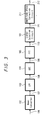
- FIGS. 3 through 6 components corresponding to FIGS. 1 and 2A to 2E described as an example of the conventional technique are denoted by like reference numerals and detailed description thereof will be omitted.
- FIG. 3 is a diagram showing the configuration of a receiving circuit of the present example.
- a signal 106 fed from an antenna or an amplifier undergoes frequency conversion in a down converter 102 to produce an intermediate frequency signal or a baseband signal.
- a frequency converted signal 107 therefrom is supplied to a low-pass filter 103.
- carrier components and so on are removed to produce an OFDM wave 108 which is a multi-carrier signal.
- This OFDM wave 108 is a multi-carrier signal containing signals in a certain carrier interval (i.e., the above described band slot interval).
- the OFDM wave 108 is converted to a digital signal in an analog/digital converter 104. Converted data are supplied to an FFT circuit 105. In the analog/digital converter 104, oversampling twice the number of carriers is conducted. The FFT 105 conducts processing for converting an inputted signal 109 formed in a time sequence to a signal 110 on a frequency sequence. The signal 110 on the frequency sequence is selected by a signal selection circuit 101 to produce a selected signal 111. In the signal selection circuit, processing of selecting information contained in half carriers of the output of the FFT 105 is conducted. The configuration so far is the same as that of the conventional receiving circuit shown in FIG. 1.
- the signal 111 outputted by the signal selection circuit 101 is supplied to an amplitude-phase correction circuit 201 to produce a signal 212 corrected in amplitude and phase.
- the signal 212 outputted by the amplitude-phase correction circuit 201 is used as a received symbol.
- the configuration of the amplitude-phase correction circuit 201 is shown in FIG. 4.
- the amplitude-phase correction circuit 201 is formed by a correction value storing memory 301 and a multiplier 302.
- the correction value storing memory 301 stores a value calculated beforehand from the amplitude characteristics and the phase characteristics of the low-pass filter 103 so as to cancel those characteristics at carrier frequencies containing the information.
- Each symbol which is the signal 111 outputted by the signal selection circuit 101 is supplied to the multiplier 302 and is multiplied by the amplitude-phase correction value stored in the correction value storing memory 301.
- each of the input signal, the output signal, and the correction value to the multiplier 302 is a signal of a complex number having a real part component and an imaginary part component.
- multiplication multiplication of complex numbers is conducted.
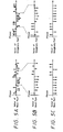
- FIGS. 5A to 5C are diagrams showing a processing conducted by the circuit of the embodiment. It is now assumed that a symbol sequence oversampled with a doubled rate as shown in FIG. 5A is outputted from the FFT 105 as the signal 110.
- the signal 111 selected by the signal selection circuit 101 becomes a signal thinned to 1/2 (only the sample points at the center are extracted as shown in FIG. 5B.
- the amplitude-phase characteristics of the low-pass filter 103 are characteristics shown in FIG. 6A.
- such characteristics as to cancel the amplitude characteristic and the phase characteristic of the low-pass filter 103 i.e., as to make those characteristics flat
- FIG. 6B there are shown characteristics canceling the amplitude characteristic and the phase characteristic of the low-pass filter 103 corresponding to the characteristics of FIG. 6A. It is sufficient for the amplitude-phase correction circuit 211 needs to have the characteristics shown in FIG. 6B.
- the actual symbol sequence is formed by a real part component and an imaginary part component. As shown in FIG. 6C, therefore, the characteristics of FIG. 6B are represented by a real part component and an imaginary part component. Sampling values respectively of the real part component and the imaginary part in positions where carriers are present are stored in the memory 301.
- a symbol sequence as shown in FIG. 6D is inputted to the amplitude-phase correction circuit 211, an ideal signal is thus obtained as corrected values as shown in FIG. 6E.
- the input signal of the amplitude-phase correction circuit connected after the FFT is multiplied by the values calculated beforehand so as to reflect the characteristics opposite to those of the low-pass filter.
- the rotation of the phase and the dispersion of the amplitude in the pass band of the low-pass filter can be suppressed.
- the points extracted by the signal selection circuit 101 it needs only be linked to the oversampling conducted in the analog/digital converter 104. It is not limited to the above described 1/2 and 2 times, but 1/3 and 3 times, and 1/4 and 4 times may also be used.
- corresponding processing may be conducted in the omitted circuit configuration of the signal selection circuit 101.
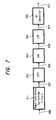
- FIG. 7 This example is an example of application to a transmitting circuit of the OFDM wave which is a multi-carrier signal. Its configuration will now be described.
- a transmitted symbol sequence 406 is converted to a signal 407 corrected in amplitude and phase by an amplitude-phase correction circuit 411.
- the signal 407 is supplied to an inverse fast Fourier transform circuit (IFFT) 405 for conversion to a multi-carrier signal.
- IFFT inverse fast Fourier transform circuit
- the signal 407 of a symbol sequence arranged on the frequency axis is thus converted to a multi-carrier signal 408 which is a discrete signal arranged on the time axis.
- This multi-carrier signal 408 is converted to a signal 409 by a digital/analog converter 404.
- the signa is then supplied to a low-pass filter 403.
- An output 410 of this low-pass filter 403 is supplied to an up converter 402 and modulated on a carrier wave to produce a transmission signal 412.
- the transmission signal 412 is radio-transmitted from an antenna (not illustrated).
- Correction values of the amplitude and phase stored in the amplitude-phase correction value 411 are values for correcting the characteristics of the low-pass filter 403.
- the output signal of the low-pass filter 403 becomes an OFDM wave obtained by ideally conducting transmission processing on the symbol sequence to be transmitted.
- the subjects of correction in the amplitude-phase correction circuit are pass band characteristics of the low-pass filter.
- the amplitude and phase of another circuit can also be corrected so long as its characteristics are known beforehand and its characteristics do not change.
- the amplitude-phase correction circuit of the present invention According to the amplitude-phase correction circuit of the present invention, deviations caused in amplitude and phase at the time of filtering in a filter are corrected. Therefore, information contained in the multi-carrier signal which is a transmitted signal is transmitted accurately and hence favorable communication can be conducted.
- a received symbol corrected in deviations caused in amplitude and phase when a received signal is filtered by a filter is obtained. This results in an effect that information contained in a multi-carrier signal can be received accurately.
- a transmitting device of the present invention deviations caused in amplitude and phase when a signal to be transmitted is filtered by a filter are corrected beforehand. In information contained in a multi-carrier signal to be transmitted, therefore, there occur no deviations in amplitude and phase caused by the influence of the filter. This results in an effect that a favorable signal scanning be transmitted.
Landscapes
- Engineering & Computer Science (AREA)
- Computer Networks & Wireless Communication (AREA)
- Signal Processing (AREA)
- Physics & Mathematics (AREA)
- Discrete Mathematics (AREA)
- General Physics & Mathematics (AREA)
- Mathematical Physics (AREA)
- Digital Transmission Methods That Use Modulated Carrier Waves (AREA)
- Cable Transmission Systems, Equalization Of Radio And Reduction Of Echo (AREA)
Applications Claiming Priority (3)
| Application Number | Priority Date | Filing Date | Title |
|---|---|---|---|
| JP222934/96 | 1996-08-23 | ||
| JP22293496 | 1996-08-23 | ||
| JP8222934A JPH1065588A (ja) | 1996-08-23 | 1996-08-23 | 振幅・位相補正回路、受信装置及び送信装置 |
Publications (2)
| Publication Number | Publication Date |
|---|---|
| EP0825743A2 true EP0825743A2 (de) | 1998-02-25 |
| EP0825743A3 EP0825743A3 (de) | 2001-02-07 |
Family
ID=16790165
Family Applications (1)
| Application Number | Title | Priority Date | Filing Date |
|---|---|---|---|
| EP97306465A Ceased EP0825743A3 (de) | 1996-08-23 | 1997-08-22 | Vorverzerrung für Mehrträgersender |
Country Status (4)
| Country | Link |
|---|---|
| US (1) | US6070056A (de) |
| EP (1) | EP0825743A3 (de) |
| JP (1) | JPH1065588A (de) |
| KR (2) | KR100538986B1 (de) |
Families Citing this family (7)
| Publication number | Priority date | Publication date | Assignee | Title |
|---|---|---|---|---|
| JP4284774B2 (ja) * | 1999-09-07 | 2009-06-24 | ソニー株式会社 | 送信装置、受信装置、通信システム、送信方法及び通信方法 |
| EP1148659B1 (de) * | 2000-04-18 | 2005-07-27 | Sony International (Europe) GmbH | OFDM Diversity-Übertragung |
| US20030128660A1 (en) * | 2002-01-09 | 2003-07-10 | Atsushi Ito | OFDM communications apparatus, OFDM communications method, and OFDM communications program |
| WO2006014142A1 (en) * | 2004-08-03 | 2006-02-09 | Agency For Science, Technology And Research | Method for detecting a signal, detector and computer program product |
| FR2890808A1 (fr) * | 2005-09-13 | 2007-03-16 | France Telecom | Caracterisation de spectre pour equipements de communication |
| KR100837114B1 (ko) | 2006-10-30 | 2008-06-11 | 지씨티 세미컨덕터 인코포레이티드 | 오버샘플링 아날로그-디지털 변환기를 이용한 다중 복조경로 ofdm 수신회로 |
| CN101599941B (zh) * | 2009-04-24 | 2012-05-30 | 新邮通信设备有限公司 | 一种正交频分复用信号的产生方法和装置 |
Family Cites Families (12)
| Publication number | Priority date | Publication date | Assignee | Title |
|---|---|---|---|---|
| NL7213388A (de) * | 1971-12-01 | 1974-04-08 | ||
| JPH01314006A (ja) * | 1988-06-13 | 1989-12-19 | Fujitsu Ltd | 歪補償回路 |
| US4943980A (en) * | 1989-05-02 | 1990-07-24 | Intelligent Modem Corporation | Multi-carrier high speed modem |
| JPH042226A (ja) * | 1990-04-19 | 1992-01-07 | Nec Corp | 通信システムにおける自動等化システム |
| US5128964A (en) * | 1990-10-10 | 1992-07-07 | Intelligent Modem Corporation | Modulation method and apparatus for multicarrier data transmission |
| KR930001563A (ko) * | 1991-06-29 | 1993-01-16 | 정용문 | 위상편차 검출 및 보상방법 |
| JP2781946B2 (ja) * | 1993-04-27 | 1998-07-30 | シャープ株式会社 | 直交周波数分割多重信号発生器 |
| SE9302453L (sv) * | 1993-07-20 | 1994-10-17 | Telia Ab | Förfarande och anordning för synkronisering i digitalt transmissionssystem av typen OFDM |
| US5444697A (en) * | 1993-08-11 | 1995-08-22 | The University Of British Columbia | Method and apparatus for frame synchronization in mobile OFDM data communication |
| KR100316736B1 (ko) * | 1993-09-27 | 2002-02-19 | 구자홍 | 동기및비동기복합수신장치 |
| JP3421880B2 (ja) * | 1994-10-05 | 2003-06-30 | ソニー株式会社 | 復調装置 |
| JPH09223990A (ja) * | 1996-02-19 | 1997-08-26 | Fujitsu Ltd | 伝送装置 |
-
1996
- 1996-08-23 JP JP8222934A patent/JPH1065588A/ja active Pending
-
1997
- 1997-08-13 US US08/910,661 patent/US6070056A/en not_active Expired - Lifetime
- 1997-08-14 KR KR1019970038866A patent/KR100538986B1/ko not_active Expired - Fee Related
- 1997-08-22 EP EP97306465A patent/EP0825743A3/de not_active Ceased
-
2005
- 2005-03-18 KR KR1020050022880A patent/KR100554048B1/ko not_active Expired - Fee Related
Also Published As
| Publication number | Publication date |
|---|---|
| KR100538986B1 (ko) | 2006-03-17 |
| KR19980018689A (ko) | 1998-06-05 |
| KR100554048B1 (ko) | 2006-02-22 |
| EP0825743A3 (de) | 2001-02-07 |
| US6070056A (en) | 2000-05-30 |
| JPH1065588A (ja) | 1998-03-06 |
Similar Documents
| Publication | Publication Date | Title |
|---|---|---|
| EP2315386B1 (de) | OFDM-Kommunikationsverfahren und -vorrichtung | |
| US7139536B2 (en) | Method and apparatus for I/Q imbalance calibration of a transmitter system | |
| JP4149044B2 (ja) | ディジタル多重搬送波信号の位相及び/又は周波数誤差を訂正する方法及び回路装置 | |
| US5406551A (en) | Method and apparatus for digital signal transmission using orthogonal frequency division multiplexing | |
| US5241544A (en) | Multi-channel tdm communication system slot phase correction | |
| EP0772330A2 (de) | Empfänger und Empfangsverfahren für OFDM-Signale | |
| EP1172983A2 (de) | Trägerrückgewinnung in Mehrträgersystemen | |
| JPH08510603A (ja) | Ofdm受信機における局所発振器エラーの補償 | |
| JPH06505852A (ja) | 直交振幅変調同期方法 | |
| EP1079577A2 (de) | Mehrträgermodulation | |
| US7123896B2 (en) | Method and apparatus for I/Q mismatch calibration in a receiver | |
| US20200412458A1 (en) | Front-end circuit | |
| US7016426B1 (en) | Method for determining the amplitude imbalance at the receiving end and quadrature error in a multi-carrier system | |
| US20050041754A1 (en) | Method and appatatus for I/Q mismatch calibration of transmitter | |
| US6070056A (en) | Amplitude-phase correction circuit, receiving device and transmitting device | |
| JPH07226724A (ja) | Ofdm変調方法及びofdm復調方法並びにofdm変調装置及びofdm復調装置 | |
| US6643339B1 (en) | Receiver and receiving method | |
| EP1170918A1 (de) | Verfahren und Einrichtung zur Erzeugung eines orthogonalen Frequenzmultiplexsignals (OFDM) | |
| EP1143677A2 (de) | Quadraturmodulation | |
| JPH11289312A (ja) | マルチキャリア無線通信装置 | |
| JP3592783B2 (ja) | 伝送路等化器 | |
| JP3583013B2 (ja) | 復調装置 | |
| JPH114208A (ja) | Ofdm伝送方法及びofdm伝送装置 | |
| JP3541653B2 (ja) | 受信信号補正方式及び直交周波数分割多重信号伝送装置 | |
| JP2002314501A (ja) | Ofdm送信装置 |
Legal Events
| Date | Code | Title | Description |
|---|---|---|---|
| PUAI | Public reference made under article 153(3) epc to a published international application that has entered the european phase |
Free format text: ORIGINAL CODE: 0009012 |
|
| AK | Designated contracting states |
Kind code of ref document: A2 Designated state(s): DE FI FR GB IT NL SE |
|
| PUAL | Search report despatched |
Free format text: ORIGINAL CODE: 0009013 |
|
| AK | Designated contracting states |
Kind code of ref document: A3 Designated state(s): AT BE CH DE DK ES FI FR GB GR IE IT LI LU MC NL PT SE |
|
| 17P | Request for examination filed |
Effective date: 20010710 |
|
| AKX | Designation fees paid |
Free format text: DE FI FR GB IT NL SE |
|
| RAP1 | Party data changed (applicant data changed or rights of an application transferred) |
Owner name: SONY CORPORATION |
|
| 17Q | First examination report despatched |
Effective date: 20040603 |
|
| STAA | Information on the status of an ep patent application or granted ep patent |
Free format text: STATUS: THE APPLICATION HAS BEEN REFUSED |
|
| 18R | Application refused |
Effective date: 20051216 |