EP0826434A1 - Verfahren und Vorrichtung zur Herstellung von dünnen Filmen aus Polymeren oder Verbundmaterialien auf verschiedenen Substraten - Google Patents
Verfahren und Vorrichtung zur Herstellung von dünnen Filmen aus Polymeren oder Verbundmaterialien auf verschiedenen Substraten Download PDFInfo
- Publication number
- EP0826434A1 EP0826434A1 EP96830429A EP96830429A EP0826434A1 EP 0826434 A1 EP0826434 A1 EP 0826434A1 EP 96830429 A EP96830429 A EP 96830429A EP 96830429 A EP96830429 A EP 96830429A EP 0826434 A1 EP0826434 A1 EP 0826434A1
- Authority
- EP
- European Patent Office
- Prior art keywords
- homogeneous
- precursors
- evaporation
- film
- polyimide
- Prior art date
- Legal status (The legal status is an assumption and is not a legal conclusion. Google has not performed a legal analysis and makes no representation as to the accuracy of the status listed.)
- Granted
Links
- 239000000758 substrate Substances 0.000 title claims abstract description 47
- 238000000034 method Methods 0.000 title claims abstract description 37
- 230000008569 process Effects 0.000 title claims abstract description 37
- 239000010409 thin film Substances 0.000 title claims abstract description 11
- 229920000642 polymer Polymers 0.000 title claims description 11
- 239000002131 composite material Substances 0.000 title description 4
- 238000001704 evaporation Methods 0.000 claims abstract description 30
- 230000008020 evaporation Effects 0.000 claims abstract description 30
- 239000010408 film Substances 0.000 claims abstract description 25
- 229920001721 polyimide Polymers 0.000 claims abstract description 24
- 239000004642 Polyimide Substances 0.000 claims abstract description 19
- 229910052751 metal Inorganic materials 0.000 claims abstract description 17
- 239000002184 metal Substances 0.000 claims abstract description 17
- 238000010438 heat treatment Methods 0.000 claims abstract description 13
- 150000002739 metals Chemical class 0.000 claims abstract description 13
- 239000007787 solid Substances 0.000 claims abstract description 13
- 239000000126 substance Substances 0.000 claims abstract description 9
- 230000008021 deposition Effects 0.000 claims abstract description 8
- 239000011521 glass Substances 0.000 claims abstract description 8
- 229910052809 inorganic oxide Inorganic materials 0.000 claims abstract description 7
- 229910052755 nonmetal Inorganic materials 0.000 claims abstract description 7
- 150000002843 nonmetals Chemical class 0.000 claims abstract description 7
- 239000012298 atmosphere Substances 0.000 claims abstract description 5
- 239000012704 polymeric precursor Substances 0.000 claims abstract description 5
- 230000006641 stabilisation Effects 0.000 claims abstract description 5
- 238000011105 stabilization Methods 0.000 claims abstract description 5
- 238000007738 vacuum evaporation Methods 0.000 claims abstract description 5
- 239000002243 precursor Substances 0.000 claims description 26
- 238000002844 melting Methods 0.000 claims description 25
- 230000008018 melting Effects 0.000 claims description 25
- 239000000203 mixture Substances 0.000 claims description 14
- GTDPSWPPOUPBNX-UHFFFAOYSA-N ac1mqpva Chemical compound CC12C(=O)OC(=O)C1(C)C1(C)C2(C)C(=O)OC1=O GTDPSWPPOUPBNX-UHFFFAOYSA-N 0.000 claims description 13
- 239000000463 material Substances 0.000 claims description 10
- 238000000151 deposition Methods 0.000 claims description 9
- 229910000831 Steel Inorganic materials 0.000 claims description 7
- GCAIEATUVJFSMC-UHFFFAOYSA-N benzene-1,2,3,4-tetracarboxylic acid Chemical compound OC(=O)C1=CC=C(C(O)=O)C(C(O)=O)=C1C(O)=O GCAIEATUVJFSMC-UHFFFAOYSA-N 0.000 claims description 7
- 239000010959 steel Substances 0.000 claims description 7
- HLBLWEWZXPIGSM-UHFFFAOYSA-N 4-Aminophenyl ether Chemical compound C1=CC(N)=CC=C1OC1=CC=C(N)C=C1 HLBLWEWZXPIGSM-UHFFFAOYSA-N 0.000 claims description 6
- 238000003486 chemical etching Methods 0.000 claims description 5
- 238000007669 thermal treatment Methods 0.000 claims description 5
- 230000001747 exhibiting effect Effects 0.000 claims description 4
- 238000000926 separation method Methods 0.000 claims description 4
- CJAOGUFAAWZWNI-UHFFFAOYSA-N 1-n,1-n,4-n,4-n-tetramethylbenzene-1,4-diamine Chemical compound CN(C)C1=CC=C(N(C)C)C=C1 CJAOGUFAAWZWNI-UHFFFAOYSA-N 0.000 claims description 3
- JVERADGGGBYHNP-UHFFFAOYSA-N 5-phenylbenzene-1,2,3,4-tetracarboxylic acid Chemical compound OC(=O)C1=C(C(O)=O)C(C(=O)O)=CC(C=2C=CC=CC=2)=C1C(O)=O JVERADGGGBYHNP-UHFFFAOYSA-N 0.000 claims description 3
- 239000011248 coating agent Substances 0.000 claims description 3
- 238000000576 coating method Methods 0.000 claims description 3
- 239000011810 insulating material Substances 0.000 claims description 3
- 230000005855 radiation Effects 0.000 claims description 3
- 230000008859 change Effects 0.000 claims description 2
- 230000007797 corrosion Effects 0.000 claims description 2
- 238000005260 corrosion Methods 0.000 claims description 2
- 239000002861 polymer material Substances 0.000 claims 3
- 239000002905 metal composite material Substances 0.000 claims 2
- 230000006866 deterioration Effects 0.000 claims 1
- 230000007613 environmental effect Effects 0.000 claims 1
- 239000002245 particle Substances 0.000 claims 1
- 229910052782 aluminium Inorganic materials 0.000 abstract description 4
- 229910052799 carbon Inorganic materials 0.000 abstract description 3
- 229910052719 titanium Inorganic materials 0.000 abstract description 3
- 238000010586 diagram Methods 0.000 description 8
- VYPSYNLAJGMNEJ-UHFFFAOYSA-N Silicium dioxide Chemical compound O=[Si]=O VYPSYNLAJGMNEJ-UHFFFAOYSA-N 0.000 description 7
- XUIMIQQOPSSXEZ-UHFFFAOYSA-N Silicon Chemical compound [Si] XUIMIQQOPSSXEZ-UHFFFAOYSA-N 0.000 description 6
- 230000004048 modification Effects 0.000 description 5
- 238000012986 modification Methods 0.000 description 5
- 230000003287 optical effect Effects 0.000 description 4
- 238000002360 preparation method Methods 0.000 description 4
- 229910052681 coesite Inorganic materials 0.000 description 3
- 229910052802 copper Inorganic materials 0.000 description 3
- 239000010949 copper Substances 0.000 description 3
- 229910052906 cristobalite Inorganic materials 0.000 description 3
- 229920003223 poly(pyromellitimide-1,4-diphenyl ether) Polymers 0.000 description 3
- 239000000377 silicon dioxide Substances 0.000 description 3
- 229910052682 stishovite Inorganic materials 0.000 description 3
- 229910052905 tridymite Inorganic materials 0.000 description 3
- KRHYYFGTRYWZRS-UHFFFAOYSA-N Fluorane Chemical compound F KRHYYFGTRYWZRS-UHFFFAOYSA-N 0.000 description 2
- PNEYBMLMFCGWSK-UHFFFAOYSA-N aluminium oxide Inorganic materials [O-2].[O-2].[O-2].[Al+3].[Al+3] PNEYBMLMFCGWSK-UHFFFAOYSA-N 0.000 description 2
- 238000004458 analytical method Methods 0.000 description 2
- 239000000919 ceramic Substances 0.000 description 2
- 229910052593 corundum Inorganic materials 0.000 description 2
- 238000005516 engineering process Methods 0.000 description 2
- 238000005259 measurement Methods 0.000 description 2
- 239000012299 nitrogen atmosphere Substances 0.000 description 2
- 239000008188 pellet Substances 0.000 description 2
- 230000009467 reduction Effects 0.000 description 2
- 238000011160 research Methods 0.000 description 2
- 238000004621 scanning probe microscopy Methods 0.000 description 2
- 125000006850 spacer group Chemical group 0.000 description 2
- 229910001845 yogo sapphire Inorganic materials 0.000 description 2
- RYGMFSIKBFXOCR-UHFFFAOYSA-N Copper Chemical compound [Cu] RYGMFSIKBFXOCR-UHFFFAOYSA-N 0.000 description 1
- 241000512668 Eunectes Species 0.000 description 1
- 229920006362 Teflon® Polymers 0.000 description 1
- 229920001646 UPILEX Polymers 0.000 description 1
- 239000004411 aluminium Substances 0.000 description 1
- XAGFODPZIPBFFR-UHFFFAOYSA-N aluminium Chemical compound [Al] XAGFODPZIPBFFR-UHFFFAOYSA-N 0.000 description 1
- 230000033228 biological regulation Effects 0.000 description 1
- 238000010276 construction Methods 0.000 description 1
- 239000000498 cooling water Substances 0.000 description 1
- 239000013078 crystal Substances 0.000 description 1
- 230000003628 erosive effect Effects 0.000 description 1
- ANSXAPJVJOKRDJ-UHFFFAOYSA-N furo[3,4-f][2]benzofuran-1,3,5,7-tetrone Chemical compound C1=C2C(=O)OC(=O)C2=CC2=C1C(=O)OC2=O ANSXAPJVJOKRDJ-UHFFFAOYSA-N 0.000 description 1
- 239000007789 gas Substances 0.000 description 1
- 239000007970 homogeneous dispersion Substances 0.000 description 1
- 238000007654 immersion Methods 0.000 description 1
- 238000009776 industrial production Methods 0.000 description 1
- 238000002329 infrared spectrum Methods 0.000 description 1
- 238000009413 insulation Methods 0.000 description 1
- 229920002521 macromolecule Polymers 0.000 description 1
- 238000004519 manufacturing process Methods 0.000 description 1
- 238000004377 microelectronic Methods 0.000 description 1
- 238000001000 micrograph Methods 0.000 description 1
- 230000000877 morphologic effect Effects 0.000 description 1
- 230000010355 oscillation Effects 0.000 description 1
- 229910052697 platinum Inorganic materials 0.000 description 1
- 229920006254 polymer film Polymers 0.000 description 1
- 239000010453 quartz Substances 0.000 description 1
- 238000005001 rutherford backscattering spectroscopy Methods 0.000 description 1
- 229910052594 sapphire Inorganic materials 0.000 description 1
- 239000010980 sapphire Substances 0.000 description 1
- 239000004065 semiconductor Substances 0.000 description 1
- 238000001228 spectrum Methods 0.000 description 1
- 238000004381 surface treatment Methods 0.000 description 1
- 238000012360 testing method Methods 0.000 description 1
- 238000000411 transmission spectrum Methods 0.000 description 1
- 230000004580 weight loss Effects 0.000 description 1
Images


Classifications
-
- B—PERFORMING OPERATIONS; TRANSPORTING
- B05—SPRAYING OR ATOMISING IN GENERAL; APPLYING FLUENT MATERIALS TO SURFACES, IN GENERAL
- B05D—PROCESSES FOR APPLYING FLUENT MATERIALS TO SURFACES, IN GENERAL
- B05D1/00—Processes for applying liquids or other fluent materials
- B05D1/60—Deposition of organic layers from vapour phase
-
- C—CHEMISTRY; METALLURGY
- C23—COATING METALLIC MATERIAL; COATING MATERIAL WITH METALLIC MATERIAL; CHEMICAL SURFACE TREATMENT; DIFFUSION TREATMENT OF METALLIC MATERIAL; COATING BY VACUUM EVAPORATION, BY SPUTTERING, BY ION IMPLANTATION OR BY CHEMICAL VAPOUR DEPOSITION, IN GENERAL; INHIBITING CORROSION OF METALLIC MATERIAL OR INCRUSTATION IN GENERAL
- C23C—COATING METALLIC MATERIAL; COATING MATERIAL WITH METALLIC MATERIAL; SURFACE TREATMENT OF METALLIC MATERIAL BY DIFFUSION INTO THE SURFACE, BY CHEMICAL CONVERSION OR SUBSTITUTION; COATING BY VACUUM EVAPORATION, BY SPUTTERING, BY ION IMPLANTATION OR BY CHEMICAL VAPOUR DEPOSITION, IN GENERAL
- C23C14/00—Coating by vacuum evaporation, by sputtering or by ion implantation of the coating forming material
- C23C14/06—Coating by vacuum evaporation, by sputtering or by ion implantation of the coating forming material characterised by the coating material
- C23C14/12—Organic material
Definitions
- the present invention relates to a process and an apparatus for preparing thin films of polyimide polymers, hereinafter referred to as FIPOL I, FIPOL II and FIPOL III for the sake of brevity, on a solid substrate of various chemical composition for the modification of chemical-physical surface characteristics of such a substrate.
- solid substrates such as, for example, inorganic oxides such as glass, SiO 2 , Al 2 O 3 or metals such as Ti, Cu, Al or non-metals such as Si, C, Ge may be used.
- Said polyimide polymers differ in structure and morphology from the polyimides already chemically produced by Dupont De Nemours and by UBE and known under the trademarks KAPTON® and UPILEX®, even if they have similar chemical formula.
- the surface deposits provided by the described process may be advantageously used for the protection of metal objects since such a process allows homogeneous controlled-thickness films to be prepared irrespective of the geometric form and the nature of the substrate.
- chemically inert polymeric films stable up to 400°C are concerned, the process allows the fields of application of said materials modified in their mechanical, electrical, optical surface characteristics to be advantageously extended.
- Another field of application relates to the preparation of polyimide-metal surface deposits by one and only process of providing films having a typical conductivity of a semiconductor, then adapted in micro-electronics and electrostatics.
- a composite material is referred to as CONPOL (registered trademark by the Applicant) in the following description.
- CONPOL registered trademark by the Applicant
- the above-cited fields of application of the invention are only some of the main fields indicated by way of a not limiting example of the invention since the process, the used materials, the organic, metal and organometal precursors, as described and claimed later on, may be advantageously used in any other equivalent field in which polyimide deposits modified or not by means of metals are produced on solid substrates to cause a permanent modification of the surface characteristics. Processes of such a type are known.
- the main object of the present invention is of overcoming the above-complained problems and limitations by a process which allows compact polyimide films such as the so-called FIPOL I, FIPOL II, FIPOL III and compositions thereof with metals to be provided by a controlled-thickness process for the modification of the chemical-physical surface characteristics of solid substrates of various kind without any limitations of the treated surface area.
- a second object of the present invention is of providing deposits having half-insulation characteristics on varying-geometry substrates by one and only process.
- a further object of the present invention is of providing polyimide films FIPOL I, FIPOL II, FIPOL III having no internal separation surfaces or cracks and exhibiting the same mechanical characteristics and the same surface tension values, chemical etching resistance and thermal endurance as the massive polyimide materials.
- FIPOL I, FIPOL II and FIPOL III on a solid substrate of various nature, particularly those based upon inorganic oxide such as, for example, glass, SiO 2 , Al 2 O 3 or metals such as Ti, Cu, Al or non-metals such as Si, C, Ge, comprising the steps of:
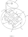
- a first aspect of the invention provides that the heating for the evaporation of the precursors takes place under a temperature control system. Particularly, such a control is carried out by using a series of melting pots placed within a vacuum chamber and having a particular geometry and being provided with their own heating means for a controlled-temperature heating.
- a second aspect of the invention provides the change of the distance between melting pot and substrate to be coated by a suitable mechanical device.
- a third aspect of the invention provides the controlled evaporation of the polymeric precursors simultaneously to that of the organometal compositions, the low-melting-point metals, and other chemical compositions which can be sublimed.
- a further aspect of the invention provides the polyimide film thickness control by controlling the evaporation time.
- the invention makes use of an apparatus including a vacuum chamber provided with a series of melting pots of suitable geometry for the evaporation of the precursors, such melting pots being provided with an automatic temperature control system, melting pot-substrate distance setting means, and evaporation time control means.
- the device for carrying out the process according to the invention essentially includes:
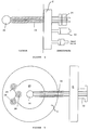
- the vacuum chamber of Fig. 1 is used for the surface treatment of samples having a surface area of about 100 cm 2 .
- the precursors of polyimide FIPOL I (benzentetracarboxylic dianhydride and 4,4'-oxydianiline) are placed into three melting pots shown in Figs. 2 and 6.
- the distance between melting pots and the surface of the substrate to be treated may be gradually set by the mechanical device formed of plate 26, rods 28 and worm screw 30.
- the substrate is polycrystalline silicium.
- Said melting pots were preliminarily filled with benzentetracarboxylic dianhydride, heated at different temperatures up to a maximum of 220°C, and kept at each temperature for a period of 120 minutes.
- the used substrate was a quartz crystal acting as sensor of the deposited thickness according to the oscillation frequency variations.
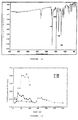
- the deposition rates according to the temperature were thus obtained as shown in Fig. 6, curve a.
- the same process was applied to the other precursor and curve b of Fig. 7 was obtained.
- the temperature of 182°C is the experimental parameter at which the molar evaporation rates of the two precursors are the same.
- Deposits of the two precursors in times varying from 70 to 360 minutes were carried out on the substrate of polycrystalline silicium.
- the diagram of the thickness vs. the time is shown in Fig. 9.
- the homogeneity of the deposit was proved by carrying out measurements of thickness transversally to the central axis of evaporation, the three melting pots being placed on the same axis over a length of 8 cm. The result is shown in Fig. 8 in which the distance between melting pot and substrate is 6 cm.
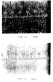
- FIG. 10 shows a photogram obtained by electronic scanning microscopy showing the surface magnified 23739 times without discontinuities or cracks (the scratch which may be seen was intentionally made as reference for the focusing).
- the comparison between FIPOL I and KAPTON (registered trademark by Dupont de Nemours) as far as the morphological surface homogeneity is concerned is shown in Figs. 13A and 13B in which two pictures obtained by an optical 10-magnification microscope (1 graduation of the ruler corresponds to 10 microns) are shown.
- Fig. 11 shows the IR spectrum of a deposit of FIPOL I on the surface of a pellet of KBr under the above-mentioned conditions relating to the evaporation of the precursors and the next thermal treatment.
- a deposit of a composite material FIPOL I-Pt was carried out on polycrystalline silicium with simultaneous deposition of the precursors (benzentetracarboxylic dianhydride and 4,4'-oxydianiline) and Pt (1,5 C 8 H 12 )C 12 .
- the Pt composition was sublimed in advance without other components and an evaporation rate of 5 nm/h at 205°C was obtained.
- a film on a sapphire was produced through simultaneous evaporation of said composition, placed in the central melting pot at 205°C, and the two precursors of FIPOL I, placed in the side melting pots at 182°C.
- Such a film subjected to a thermal treatment under N 2 for 2 hours at 250°C is a homogeneous dispersion of Pt in FIPOL I (Fig. 7) as ascertained by RBS analysis (Rutherford Backscattering Spectrometry).
- the atomic ratio between Pt and C is about 1/28.
- Such a material was referred to as CONPOL.
- Samples of such a material were subjected to measurements of electrical surface resistivity and the results are shown in Fig. 14.
- the surface resistivity becomes stable after about 60 minutes and reaches the typical values of the half-insulating materials.
- the non-ohmic characteristics are shown in the same figure.
- Fig. 14 shows the weight loss according to the immersion time. In the same figure there is shown the same relationship for a like glass cylinder not coated with polyimide.
- the results shown in the figures confirm the advantages of the process for providing surface deposits of the present invention.
- the preparation of the surface deposits of composite materials finds a wide application with reference to parts of radiation detectors such as the microstrip gas chambers and the microgap chambers since it is possible to deposit films on a very great number of different substrates: the polymer film assures a chemical-physical stability for the substrate against corrosion and damages due to radiations by modifying the wettability and the electrical-mechanical surface characteristics.
- the present invention is described and illustrated on the base of a preferred embodiment thereof. It should be understood that a number of construction modifications and changes may be made by those skilled in the art without departing from the scope of the present industrial invention as defined in the following claims.
Landscapes
- Chemical & Material Sciences (AREA)
- Chemical Kinetics & Catalysis (AREA)
- Engineering & Computer Science (AREA)
- Materials Engineering (AREA)
- Mechanical Engineering (AREA)
- Metallurgy (AREA)
- Organic Chemistry (AREA)
- Physical Vapour Deposition (AREA)
- Laminated Bodies (AREA)
- Manufacture Of Macromolecular Shaped Articles (AREA)
Priority Applications (3)
| Application Number | Priority Date | Filing Date | Title |
|---|---|---|---|
| EP96830429A EP0826434B1 (de) | 1996-07-31 | 1996-07-31 | Verfahren und Vorrichtung zur Herstellung von dünnen Filmen aus Polymeren oder Verbundmaterialien auf verschiedenen Substraten |
| AT96830429T ATE269170T1 (de) | 1996-07-31 | 1996-07-31 | Verfahren und vorrichtung zur herstellung von dünnen filmen aus polymeren oder verbundmaterialien auf verschiedenen substraten |
| DE69632730T DE69632730D1 (de) | 1996-07-31 | 1996-07-31 | Verfahren und Vorrichtung zur Herstellung von dünnen Filmen aus Polymeren oder Verbundmaterialien auf verschiedenen Substraten |
Applications Claiming Priority (1)
| Application Number | Priority Date | Filing Date | Title |
|---|---|---|---|
| EP96830429A EP0826434B1 (de) | 1996-07-31 | 1996-07-31 | Verfahren und Vorrichtung zur Herstellung von dünnen Filmen aus Polymeren oder Verbundmaterialien auf verschiedenen Substraten |
Publications (2)
| Publication Number | Publication Date |
|---|---|
| EP0826434A1 true EP0826434A1 (de) | 1998-03-04 |
| EP0826434B1 EP0826434B1 (de) | 2004-06-16 |
Family
ID=8225981
Family Applications (1)
| Application Number | Title | Priority Date | Filing Date |
|---|---|---|---|
| EP96830429A Expired - Lifetime EP0826434B1 (de) | 1996-07-31 | 1996-07-31 | Verfahren und Vorrichtung zur Herstellung von dünnen Filmen aus Polymeren oder Verbundmaterialien auf verschiedenen Substraten |
Country Status (3)
| Country | Link |
|---|---|
| EP (1) | EP0826434B1 (de) |
| AT (1) | ATE269170T1 (de) |
| DE (1) | DE69632730D1 (de) |
Cited By (3)
| Publication number | Priority date | Publication date | Assignee | Title |
|---|---|---|---|---|
| EP1382713A3 (de) * | 2002-07-19 | 2004-06-02 | Lg Electronics Inc. | Quelle zur thermischen PVD-Beschichtung für organische elektrolumineszente Schichten |
| WO2007030202A3 (en) * | 2005-07-18 | 2007-05-03 | Univ California | Preparation of membranes using solvent-less vapor deposition followed by in-situ polymerization |
| CN113529015A (zh) * | 2021-07-02 | 2021-10-22 | 中国科学院长春光学精密机械与物理研究所 | 金属有机材料的制备方法 |
Citations (10)
| Publication number | Priority date | Publication date | Assignee | Title |
|---|---|---|---|---|
| FR2297900A1 (fr) * | 1975-01-20 | 1976-08-13 | Du Pont | Procede de formation de revetements d'arret s'opposant au passage des gaz |
| US4629547A (en) * | 1983-11-16 | 1986-12-16 | Hitachi, Ltd. | Process for forming protective film of organic polymer and boron |
| EP0278629A1 (de) * | 1987-01-30 | 1988-08-17 | Hitachi Maxell Ltd. | Amorphe Werkstoffe |
| JPS63259069A (ja) * | 1987-04-16 | 1988-10-26 | Sumitomo Electric Ind Ltd | 樹脂と金属の接着方法 |
| JPS63264369A (ja) * | 1987-04-21 | 1988-11-01 | Toshiba Corp | サ−マルヘツドの製造方法 |
| EP0376333A2 (de) * | 1988-12-29 | 1990-07-04 | Sharp Kabushiki Kaisha | Verfahren und Apparatur zur Herstellung dünner Polyimid-Filme |
| JPH02282947A (ja) * | 1989-04-25 | 1990-11-20 | Seiko Epson Corp | 光磁気記録媒体とその製造方法 |
| JPH0313561A (ja) * | 1989-06-09 | 1991-01-22 | Ulvac Corp | ポリイミド樹脂被膜の形成方法 |
| JPH05265006A (ja) * | 1992-03-17 | 1993-10-15 | Sharp Corp | 液晶用配向膜の製造方法 |
| US5354636A (en) * | 1991-02-19 | 1994-10-11 | Fuji Xerox Co., Ltd. | Electrophotographic photoreceptor comprising polyimide resin |
-
1996
- 1996-07-31 EP EP96830429A patent/EP0826434B1/de not_active Expired - Lifetime
- 1996-07-31 DE DE69632730T patent/DE69632730D1/de not_active Expired - Fee Related
- 1996-07-31 AT AT96830429T patent/ATE269170T1/de not_active IP Right Cessation
Patent Citations (10)
| Publication number | Priority date | Publication date | Assignee | Title |
|---|---|---|---|---|
| FR2297900A1 (fr) * | 1975-01-20 | 1976-08-13 | Du Pont | Procede de formation de revetements d'arret s'opposant au passage des gaz |
| US4629547A (en) * | 1983-11-16 | 1986-12-16 | Hitachi, Ltd. | Process for forming protective film of organic polymer and boron |
| EP0278629A1 (de) * | 1987-01-30 | 1988-08-17 | Hitachi Maxell Ltd. | Amorphe Werkstoffe |
| JPS63259069A (ja) * | 1987-04-16 | 1988-10-26 | Sumitomo Electric Ind Ltd | 樹脂と金属の接着方法 |
| JPS63264369A (ja) * | 1987-04-21 | 1988-11-01 | Toshiba Corp | サ−マルヘツドの製造方法 |
| EP0376333A2 (de) * | 1988-12-29 | 1990-07-04 | Sharp Kabushiki Kaisha | Verfahren und Apparatur zur Herstellung dünner Polyimid-Filme |
| JPH02282947A (ja) * | 1989-04-25 | 1990-11-20 | Seiko Epson Corp | 光磁気記録媒体とその製造方法 |
| JPH0313561A (ja) * | 1989-06-09 | 1991-01-22 | Ulvac Corp | ポリイミド樹脂被膜の形成方法 |
| US5354636A (en) * | 1991-02-19 | 1994-10-11 | Fuji Xerox Co., Ltd. | Electrophotographic photoreceptor comprising polyimide resin |
| JPH05265006A (ja) * | 1992-03-17 | 1993-10-15 | Sharp Corp | 液晶用配向膜の製造方法 |
Non-Patent Citations (12)
| Title |
|---|
| DATABASE WPI Section Ch Week 9346, Derwent World Patents Index; Class A26, AN 93-362184, XP002022481 * |
| IIJMA ET AL., MACROMOLECULES., vol. 22, 1989, pages 2944 |
| J.R.SALEM ET AL.: "Solventless polyimide films by vapor deposition", JOURNAL OF VACUUM SCIENCE AND TECHNOLOGY: PART A, vol. 4, no. 3, May 1986 (1986-05-01) - June 1986 (1986-06-01), NEW YORK US, pages 369 - 374, XP002022479 * |
| LAMB ET AL., LAGMUIR., vol. 4, 1988, pages 249 |
| M. IIJIMA ET AL.: "Vapor Deposition Polymerization: A Study on Film Formation in Reaction of Pyromellitic Anhydride and Bis(4-aminophenyl) Ether", MACROMOLECULES, vol. 22, 1989, EASTON US, pages 2944 - 2946, XP002022480 * |
| PATENT ABSTRACTS OF JAPAN vol. 013, no. 060 (M - 796) 10 February 1989 (1989-02-10) * |
| PATENT ABSTRACTS OF JAPAN vol. 013, no. 069 (C - 569) 16 February 1989 (1989-02-16) * |
| PATENT ABSTRACTS OF JAPAN vol. 015, no. 051 (P - 1163) 6 February 1991 (1991-02-06) * |
| PATENT ABSTRACTS OF JAPAN vol. 015, no. 132 (C - 0819) 29 March 1991 (1991-03-29) * |
| PETHE ET AL., JOURNAL OF MATERIAL RESEARCH., vol. 8, no. 12, 1993, pages 3218 |
| SALEM ET AL., JOURNAL OF VACUUM SCIENCE & TECHNOLOGY., vol. A4, no. 3, 1986, pages 369 |
| YAMADA ET AL., JOURNAL OF VACUUM SCIENCE & TECHNOLOGY., vol. A1, no. 5, 1993, pages 2590 |
Cited By (6)
| Publication number | Priority date | Publication date | Assignee | Title |
|---|---|---|---|---|
| EP1382713A3 (de) * | 2002-07-19 | 2004-06-02 | Lg Electronics Inc. | Quelle zur thermischen PVD-Beschichtung für organische elektrolumineszente Schichten |
| US7025832B2 (en) | 2002-07-19 | 2006-04-11 | Lg Electronics Inc. | Source for thermal physical vapor deposition of organic electroluminescent layers |
| US7815737B2 (en) | 2002-07-19 | 2010-10-19 | Lg Display Co., Ltd. | Source for thermal physical vapor deposition of organic electroluminescent layers |
| WO2007030202A3 (en) * | 2005-07-18 | 2007-05-03 | Univ California | Preparation of membranes using solvent-less vapor deposition followed by in-situ polymerization |
| CN113529015A (zh) * | 2021-07-02 | 2021-10-22 | 中国科学院长春光学精密机械与物理研究所 | 金属有机材料的制备方法 |
| CN113529015B (zh) * | 2021-07-02 | 2022-10-25 | 中国科学院长春光学精密机械与物理研究所 | 金属有机材料的制备方法 |
Also Published As
| Publication number | Publication date |
|---|---|
| ATE269170T1 (de) | 2004-07-15 |
| EP0826434B1 (de) | 2004-06-16 |
| DE69632730D1 (de) | 2004-07-22 |
Similar Documents
| Publication | Publication Date | Title |
|---|---|---|
| Kuo et al. | Microstructure and thermal conductivity of epitaxial AlN thin films | |
| Maniv et al. | Controlled texture of reactively rf‐sputtered ZnO thin films | |
| Wu et al. | Effect of deposition rate on properties of YBa2Cu3O7− δ superconducting thin films | |
| Guo et al. | Ba (Mg1/3Ta2/3) O3 single crystal fiber grown by the laser heated pedestal growth technique | |
| Saraie et al. | Chemical Vapor Deposition of Al2 O 3 Thin Films under Reduced Pressures | |
| Hinds et al. | Thin films for superconducting electronics: Precursor performance issues, deposition mechanisms, and superconducting phase formation-processing strategies in the growth of Tl2Ba2CaCu2O8 films by metal-organic chemical vapor deposition | |
| Theis et al. | Epitaxial lead titanate grown by MBE | |
| Siegal et al. | Growth and characterization of Ba2YCu3O7− δ films in reduced oxygen partial pressures using the BaF2 post-annealing process | |
| Johs et al. | Preparation of high T c Tl‐Ba‐Ca‐Cu‐O thin films by pulsed laser evaporation and Tl2O3 vapor processing | |
| Cole et al. | Evaluation of Ta2O5 as a buffer layer film for integration of microwave tunable Ba1− xSrxTiO3 based thin films with silicon substrates | |
| EP0826434A1 (de) | Verfahren und Vorrichtung zur Herstellung von dünnen Filmen aus Polymeren oder Verbundmaterialien auf verschiedenen Substraten | |
| Yan et al. | Flux growth of single crystals of spinel ZnGa2O4 and CdGa2O4 | |
| JPH01153526A (ja) | ユーロピウム、バリウム、銅系酸化物の膜超伝導体 | |
| EP3957775A1 (de) | Heterostrukturmembrane und verfahren zur herstellung von heterostrukturmembranen | |
| US5554224A (en) | Substrate heater for thin film deposition | |
| Park et al. | Long length fabrication of YBCO on rolling assisted biaxially textured substrates (RABiTS) using pulsed laser deposition | |
| Trtık et al. | Study of the epitaxial growth of CeO2 (0 0 1) on yttria-stabilized zirconia/Si (0 0 1) | |
| US5653954A (en) | Nickel-manganese oxide single crystals | |
| US6803134B1 (en) | Paraelectric thin film material and method statement of government interest | |
| US6099164A (en) | Sensors incorporating nickel-manganese oxide single crystals | |
| Wood et al. | The diffusion of gold through polycrystalline silver in thin films at temperatures near 150° C | |
| Markert et al. | Structural and electrical properties of thin dc magnetron‐sputtered gold films deposited on float glass | |
| Cillessen et al. | Improved uniformity of multielement thin films prepared by off‐axis pulsed laser deposition using a new heater design | |
| US20250359483A1 (en) | Polymer-derived ceramic thin film thermocouple and preparation method thereof | |
| Wang et al. | Microstructure of Ruthenium Dioxide Films Grown on α–Al2O3 (0001), α–Al2O3 (1102), and SrTiO3 (100) Using Reactive Sputtering |
Legal Events
| Date | Code | Title | Description |
|---|---|---|---|
| PUAI | Public reference made under article 153(3) epc to a published international application that has entered the european phase |
Free format text: ORIGINAL CODE: 0009012 |
|
| AK | Designated contracting states |
Kind code of ref document: A1 Designated state(s): AT BE CH DE DK ES FI FR GB GR IE IT LI LU MC NL PT SE |
|
| AX | Request for extension of the european patent |
Free format text: AL PAYMENT 960827;LT PAYMENT 960827;LV PAYMENT 960827;SI PAYMENT 960827 |
|
| 17P | Request for examination filed |
Effective date: 19980903 |
|
| AKX | Designation fees paid |
Free format text: AT BE CH DE DK ES FI FR GB GR IE IT LI LU MC NL PT SE |
|
| AXX | Extension fees paid |
Free format text: AL PAYMENT 960827;LT PAYMENT 960827;LV PAYMENT 960827;SI PAYMENT 960827 |
|
| RBV | Designated contracting states (corrected) |
Designated state(s): AT BE CH DE DK ES FI FR GB GR IE IT LI LU MC NL PT SE |
|
| 17Q | First examination report despatched |
Effective date: 20010904 |
|
| GRAP | Despatch of communication of intention to grant a patent |
Free format text: ORIGINAL CODE: EPIDOSNIGR1 |
|
| RIN1 | Information on inventor provided before grant (corrected) |
Inventor name: PIERI, UGO Inventor name: DELLA MEA, GIANANTONIO Inventor name: CARTURAN, SARA |
|
| GRAS | Grant fee paid |
Free format text: ORIGINAL CODE: EPIDOSNIGR3 |
|
| GRAA | (expected) grant |
Free format text: ORIGINAL CODE: 0009210 |
|
| AK | Designated contracting states |
Kind code of ref document: B1 Designated state(s): AT BE CH DE DK ES FI FR GB GR IE IT LI LU MC NL PT SE |
|
| AX | Request for extension of the european patent |
Extension state: AL LT LV SI |
|
| PG25 | Lapsed in a contracting state [announced via postgrant information from national office to epo] |
Ref country code: NL Free format text: LAPSE BECAUSE OF FAILURE TO SUBMIT A TRANSLATION OF THE DESCRIPTION OR TO PAY THE FEE WITHIN THE PRESCRIBED TIME-LIMIT Effective date: 20040616 Ref country code: LI Free format text: LAPSE BECAUSE OF FAILURE TO SUBMIT A TRANSLATION OF THE DESCRIPTION OR TO PAY THE FEE WITHIN THE PRESCRIBED TIME-LIMIT Effective date: 20040616 Ref country code: IT Free format text: LAPSE BECAUSE OF FAILURE TO SUBMIT A TRANSLATION OF THE DESCRIPTION OR TO PAY THE FEE WITHIN THE PRE;WARNING: LAPSES OF ITALIAN PATENTS WITH EFFECTIVE DATE BEFORE 2007 MAY HAVE OCCURRED AT ANY TIME BEFORE 2007. THE CORRECT EFFECTIVE DATE MAY BE DIFFERENT FROM THE ONE RECORDED.SCRIBED TIME-LIMIT Effective date: 20040616 Ref country code: FR Free format text: LAPSE BECAUSE OF NON-PAYMENT OF DUE FEES Effective date: 20040616 Ref country code: FI Free format text: LAPSE BECAUSE OF FAILURE TO SUBMIT A TRANSLATION OF THE DESCRIPTION OR TO PAY THE FEE WITHIN THE PRESCRIBED TIME-LIMIT Effective date: 20040616 Ref country code: CH Free format text: LAPSE BECAUSE OF FAILURE TO SUBMIT A TRANSLATION OF THE DESCRIPTION OR TO PAY THE FEE WITHIN THE PRESCRIBED TIME-LIMIT Effective date: 20040616 Ref country code: BE Free format text: LAPSE BECAUSE OF FAILURE TO SUBMIT A TRANSLATION OF THE DESCRIPTION OR TO PAY THE FEE WITHIN THE PRESCRIBED TIME-LIMIT Effective date: 20040616 Ref country code: AT Free format text: LAPSE BECAUSE OF FAILURE TO SUBMIT A TRANSLATION OF THE DESCRIPTION OR TO PAY THE FEE WITHIN THE PRESCRIBED TIME-LIMIT Effective date: 20040616 |
|
| REG | Reference to a national code |
Ref country code: GB Ref legal event code: FG4D |
|
| REG | Reference to a national code |
Ref country code: CH Ref legal event code: EP |
|
| REF | Corresponds to: |
Ref document number: 69632730 Country of ref document: DE Date of ref document: 20040722 Kind code of ref document: P |
|
| REG | Reference to a national code |
Ref country code: IE Ref legal event code: FG4D |
|
| PG25 | Lapsed in a contracting state [announced via postgrant information from national office to epo] |
Ref country code: MC Free format text: LAPSE BECAUSE OF NON-PAYMENT OF DUE FEES Effective date: 20040731 Ref country code: LU Free format text: LAPSE BECAUSE OF NON-PAYMENT OF DUE FEES Effective date: 20040731 |
|
| PG25 | Lapsed in a contracting state [announced via postgrant information from national office to epo] |
Ref country code: IE Free format text: LAPSE BECAUSE OF NON-PAYMENT OF DUE FEES Effective date: 20040803 |
|
| PG25 | Lapsed in a contracting state [announced via postgrant information from national office to epo] |
Ref country code: SE Free format text: LAPSE BECAUSE OF FAILURE TO SUBMIT A TRANSLATION OF THE DESCRIPTION OR TO PAY THE FEE WITHIN THE PRESCRIBED TIME-LIMIT Effective date: 20040916 Ref country code: GR Free format text: LAPSE BECAUSE OF FAILURE TO SUBMIT A TRANSLATION OF THE DESCRIPTION OR TO PAY THE FEE WITHIN THE PRESCRIBED TIME-LIMIT Effective date: 20040916 Ref country code: GB Free format text: LAPSE BECAUSE OF NON-PAYMENT OF DUE FEES Effective date: 20040916 Ref country code: DK Free format text: LAPSE BECAUSE OF FAILURE TO SUBMIT A TRANSLATION OF THE DESCRIPTION OR TO PAY THE FEE WITHIN THE PRESCRIBED TIME-LIMIT Effective date: 20040916 |
|
| PG25 | Lapsed in a contracting state [announced via postgrant information from national office to epo] |
Ref country code: ES Free format text: LAPSE BECAUSE OF FAILURE TO SUBMIT A TRANSLATION OF THE DESCRIPTION OR TO PAY THE FEE WITHIN THE PRESCRIBED TIME-LIMIT Effective date: 20040927 |
|
| LTIE | Lt: invalidation of european patent or patent extension |
Effective date: 20040616 |
|
| NLV1 | Nl: lapsed or annulled due to failure to fulfill the requirements of art. 29p and 29m of the patents act | ||
| REG | Reference to a national code |
Ref country code: CH Ref legal event code: PL |
|
| PG25 | Lapsed in a contracting state [announced via postgrant information from national office to epo] |
Ref country code: DE Free format text: LAPSE BECAUSE OF NON-PAYMENT OF DUE FEES Effective date: 20050201 |
|
| PLBE | No opposition filed within time limit |
Free format text: ORIGINAL CODE: 0009261 |
|
| STAA | Information on the status of an ep patent application or granted ep patent |
Free format text: STATUS: NO OPPOSITION FILED WITHIN TIME LIMIT |
|
| GBPC | Gb: european patent ceased through non-payment of renewal fee |
Effective date: 20040916 |
|
| REG | Reference to a national code |
Ref country code: IE Ref legal event code: MM4A |
|
| 26N | No opposition filed |
Effective date: 20050317 |
|
| EN | Fr: translation not filed | ||
| PG25 | Lapsed in a contracting state [announced via postgrant information from national office to epo] |
Ref country code: PT Free format text: LAPSE BECAUSE OF NON-PAYMENT OF DUE FEES Effective date: 20041116 |