EP0826983A1 - Plaque multicouche pour imagerie à rayons X et procédé de fabrication - Google Patents
Plaque multicouche pour imagerie à rayons X et procédé de fabrication Download PDFInfo
- Publication number
- EP0826983A1 EP0826983A1 EP97306672A EP97306672A EP0826983A1 EP 0826983 A1 EP0826983 A1 EP 0826983A1 EP 97306672 A EP97306672 A EP 97306672A EP 97306672 A EP97306672 A EP 97306672A EP 0826983 A1 EP0826983 A1 EP 0826983A1
- Authority
- EP
- European Patent Office
- Prior art keywords
- selenium
- layer
- substrate
- doped
- amorphous
- Prior art date
- Legal status (The legal status is an assumption and is not a legal conclusion. Google has not performed a legal analysis and makes no representation as to the accuracy of the status listed.)
- Granted
Links
Images


Classifications
-
- H—ELECTRICITY
- H10—SEMICONDUCTOR DEVICES; ELECTRIC SOLID-STATE DEVICES NOT OTHERWISE PROVIDED FOR
- H10F—INORGANIC SEMICONDUCTOR DEVICES SENSITIVE TO INFRARED RADIATION, LIGHT, ELECTROMAGNETIC RADIATION OF SHORTER WAVELENGTH OR CORPUSCULAR RADIATION
- H10F30/00—Individual radiation-sensitive semiconductor devices in which radiation controls the flow of current through the devices, e.g. photodetectors
- H10F30/301—Individual radiation-sensitive semiconductor devices in which radiation controls the flow of current through the devices, e.g. photodetectors the devices being sensitive to very short wavelength, e.g. being sensitive to X-rays, gamma-rays or corpuscular radiation
-
- G—PHYSICS
- G01—MEASURING; TESTING
- G01T—MEASUREMENT OF NUCLEAR OR X-RADIATION
- G01T1/00—Measuring X-radiation, gamma radiation, corpuscular radiation, or cosmic radiation
- G01T1/16—Measuring radiation intensity
- G01T1/24—Measuring radiation intensity with semiconductor detectors
- G01T1/246—Measuring radiation intensity with semiconductor detectors utilizing latent read-out, e.g. charge stored and read-out later
-
- G—PHYSICS
- G03—PHOTOGRAPHY; CINEMATOGRAPHY; ANALOGOUS TECHNIQUES USING WAVES OTHER THAN OPTICAL WAVES; ELECTROGRAPHY; HOLOGRAPHY
- G03G—ELECTROGRAPHY; ELECTROPHOTOGRAPHY; MAGNETOGRAPHY
- G03G5/00—Recording-members for original recording by exposure, e.g. to light, to heat or to electrons; Manufacture thereof; Selection of materials therefor
- G03G5/02—Charge-receiving layers
- G03G5/04—Photoconductive layers; Charge-generation layers or charge-transporting layers; Additives therefor; Binders therefor
- G03G5/043—Photoconductive layers characterised by having two or more layers or characterised by their composite structure
- G03G5/0433—Photoconductive layers characterised by having two or more layers or characterised by their composite structure all layers being inorganic
-
- G—PHYSICS
- G03—PHOTOGRAPHY; CINEMATOGRAPHY; ANALOGOUS TECHNIQUES USING WAVES OTHER THAN OPTICAL WAVES; ELECTROGRAPHY; HOLOGRAPHY
- G03G—ELECTROGRAPHY; ELECTROPHOTOGRAPHY; MAGNETOGRAPHY
- G03G5/00—Recording-members for original recording by exposure, e.g. to light, to heat or to electrons; Manufacture thereof; Selection of materials therefor
- G03G5/02—Charge-receiving layers
- G03G5/04—Photoconductive layers; Charge-generation layers or charge-transporting layers; Additives therefor; Binders therefor
- G03G5/08—Photoconductive layers; Charge-generation layers or charge-transporting layers; Additives therefor; Binders therefor characterised by the photoconductive material being inorganic
- G03G5/082—Photoconductive layers; Charge-generation layers or charge-transporting layers; Additives therefor; Binders therefor characterised by the photoconductive material being inorganic and not being incorporated in a bonding material, e.g. vacuum deposited
- G03G5/08207—Selenium-based
-
- G—PHYSICS
- G03—PHOTOGRAPHY; CINEMATOGRAPHY; ANALOGOUS TECHNIQUES USING WAVES OTHER THAN OPTICAL WAVES; ELECTROGRAPHY; HOLOGRAPHY
- G03G—ELECTROGRAPHY; ELECTROPHOTOGRAPHY; MAGNETOGRAPHY
- G03G5/00—Recording-members for original recording by exposure, e.g. to light, to heat or to electrons; Manufacture thereof; Selection of materials therefor
- G03G5/14—Inert intermediate or cover layers for charge-receiving layers
- G03G5/142—Inert intermediate layers
- G03G5/144—Inert intermediate layers comprising inorganic material
-
- H—ELECTRICITY
- H10—SEMICONDUCTOR DEVICES; ELECTRIC SOLID-STATE DEVICES NOT OTHERWISE PROVIDED FOR
- H10F—INORGANIC SEMICONDUCTOR DEVICES SENSITIVE TO INFRARED RADIATION, LIGHT, ELECTROMAGNETIC RADIATION OF SHORTER WAVELENGTH OR CORPUSCULAR RADIATION
- H10F39/00—Integrated devices, or assemblies of multiple devices, comprising at least one element covered by group H10F30/00, e.g. radiation detectors comprising photodiode arrays
- H10F39/10—Integrated devices
- H10F39/12—Image sensors
- H10F39/191—Photoconductor image sensors
- H10F39/195—X-ray, gamma-ray or corpuscular radiation imagers
-
- H—ELECTRICITY
- H10—SEMICONDUCTOR DEVICES; ELECTRIC SOLID-STATE DEVICES NOT OTHERWISE PROVIDED FOR
- H10F—INORGANIC SEMICONDUCTOR DEVICES SENSITIVE TO INFRARED RADIATION, LIGHT, ELECTROMAGNETIC RADIATION OF SHORTER WAVELENGTH OR CORPUSCULAR RADIATION
- H10F77/00—Constructional details of devices covered by this subclass
- H10F77/10—Semiconductor bodies
- H10F77/16—Material structures, e.g. crystalline structures, film structures or crystal plane orientations
- H10F77/162—Non-monocrystalline materials, e.g. semiconductor particles embedded in insulating materials
- H10F77/166—Amorphous semiconductors
-
- Y—GENERAL TAGGING OF NEW TECHNOLOGICAL DEVELOPMENTS; GENERAL TAGGING OF CROSS-SECTIONAL TECHNOLOGIES SPANNING OVER SEVERAL SECTIONS OF THE IPC; TECHNICAL SUBJECTS COVERED BY FORMER USPC CROSS-REFERENCE ART COLLECTIONS [XRACs] AND DIGESTS
- Y02—TECHNOLOGIES OR APPLICATIONS FOR MITIGATION OR ADAPTATION AGAINST CLIMATE CHANGE
- Y02E—REDUCTION OF GREENHOUSE GAS [GHG] EMISSIONS, RELATED TO ENERGY GENERATION, TRANSMISSION OR DISTRIBUTION
- Y02E10/00—Energy generation through renewable energy sources
- Y02E10/50—Photovoltaic [PV] energy
Definitions
- the present invention relates to an improved multilayer plate for X-ray imaging and to a method for producing such plate, used for converting X-rays into a latent electrostatic image.
- This latent electrostatic image can subsequently be read out by various schemes, such as by a scanning laser beam, a microcapacitor active matrix panel, or a bank of electrostatic probes.
- U.S. Patent No. 3,975,635 of Aug. 17, 1976 discloses a xeroradiographic plate consisting of a conductive backing having thereon a photoconductive layer of selenium and an intermediate layer of an alloy comprising about 15-45 wt% of arsenic and 55-85 wt% of selenium, which intermediate layer has a thickness of about 15-150 ⁇ m and is used to reduce the capacitance of the structure with the result that images are obtained which are capable of development at lower fields without substantial loss of resolution.
- U.S. Patent No. 4,286,033 of Aug 25, 1981 discloses a multilayer inorganic photosensitive device which comprises a number of various layers, one of which is a hole trapping layer consisting of a halogen doped selenium arsenic alloy wherein the amount of selenium ranges from 95-99.9 wt%, the amount of arsenic ranges from 0.1 to 5 wt% and the amount of halogen is from 10-200 ppm (parts per million).
- This hole trapping layer has a thickness of 0.01-5 ⁇ m (microns), and is used to retain positive charges at the interface between the generating layer and the overcoating insulating layer, thereby improving image quality.
- U.S. Patent No. 4,338,387 of July 6, 1982 relates to an overcoated photoreceptive device containing a layer of electron trapping material and a hole trapping layer, these layers being comprised of a halogen doped selenium arsenic alloy wherein the amount of selenium is about 95-99.9 wt%, the amount of arsenic is between 0.1-5 wt% and the amount of halogen is from 10 ppm to 200 ppm.
- U.S. Patent No. 4,770,965 of September 13, 1988 discloses a selenium alloy imaging member suitable for X-ray imaging, which is characterized by providing on the Se alloy layer a thin protective organic overcoating layer having about 0.5-3 wt% of nigrosine. This is claimed to result in a greater resolution at a significantly reduced X-ray dosage.
- the concept of using intermediate polymer adhesive primer layers between the selenium layer and the metal oxide surface is also disclosed.
- these polymer layers have high thermal expansion coefficients and are not effective in reducing the shear stress due to different thermal expansion of the various layers in the device and may result in film cracking.
- a multilayer electrophotographic photoreceptor which comprises an As 2 Se 3 carrier transport layer, a 30 to 50 wt% Te-Se alloy carrier generation layer and an As 2 Se 3 surface protection layer as well as an outer layer of a transparent insulating material and in U.S. Patent No. 5,021,310 of June 4, 1991 also assigned to Fuji Electric Co. Ltd. a further thermal expansion relieving layer comprising arsenic and selenium is provided within the photoreceptor. It is stated in this patent that the As concentration of the thermal expansion relieving layer varied from 10 wt% to 38.7 wt% and its overall thickness was 1 ⁇ m. A surface protective layer of As 2 Se 3 containing 1000 ppm of iodine was deposited thereon to a thickness of 3 ⁇ m. Again, this patent relates to an electrophotographic photoreceptor, rather than to an X-ray imaging device.
- a fairly complex X-ray image detector which comprises a plurality of X-ray sensitive sensors each of which has a collecting electrode, a reference electrode and a switching element which connects the collecting electrode to an output lead; a photoconductor layer is provided between the individual collecting electrodes and a bias electrode; and each of the collecting electrodes comprises two electrically contacting electrode portions arranged and situated in a very specific manner, so that the majority of the charge carriers generated in the photoconductor flow to the collecting electrodes.
- a-Se alloys amorphous selenium alloys
- electrophotographic or xerographic industry see, for example, U.S. Patent No. 3,041,166 of June 26, 1962
- alloying of Se with about 40 atomic % Te has been shown to decrease the effective optical band gap of selenium from 2.2eV down to about 1.2eV.
- this increased longer wavelength photosensitivity generally occurs at the expense of electrophotographic properties - high residual potentials and rapid dark decays being typical of this class of materials.
- the electrophotographic properties of a-Se x Te 1-x materials generally preclude the use of these materials in monolayer photoreceptor applications. Since photoreceptors require both low residuals, wide panchromicity (especially for laser printer applications, where low cost semiconductor lasers emit light in the long wavelength regime), and low dark decay, considerable effort was placed into decoupling the photogeneration process and the charge transport process in the device. Se x Te 1-x alloys were used to absorb the light, but since the xerographic properties of this material were not optimal, a second charge transport layer was used to achieve the desired electrophotographic properties.
- multilayer selenium based structures have also been employed for higher energy X-ray imaging applications.
- One of the earliest commercial applications of selenium to X-ray imaging was in xeroradiography, where the detector consisted of a selenium layer deposited onto an aluminum plate.
- the plate was sensitized by corona charging, exposed to the patient modulated X-ray beam to selectively discharge the selenium, and then developed by passing triboelectrically charged toner particles across the selenium plate, transferring the toner particles to paper, and finally fixing the image by heating the paper.
- the selenium plate had to be cleaned from all residual toner particles (generally by mechanical brush), and then restored to a "neutral space charge” condition.
- the multilayer structures used in optical imaging applications and those used in X-ray imaging applications are not interchangeable and have acquired separate status within the relevant art as is obvious from the prior art patents discussed above.
- the static mode there are two distinct modes of imaging, namely the static mode and the dynamic mode which may be defined as follows:
- images can only be taken at a relatively low frequency, e.g. 1 image every 20 seconds, and the X-ray beam is pulsed. As such, there is sufficient time to neutralize any space charge which accumulates in the device between images.
- images are taken at a much higher frequency, e.g. 30 images per second, and the X-ray beam is left on during the entire examination. In this case, there is no time to remove the applied bias voltage between images to allow holes to be injected from the bottom buffer layer into the bulk X-ray absorbing layer to neutralize the negative space charge.
- prior art selenium based X-ray detectors have suffered from the availability of a limited number of materials which could be used as the substrate electrode material.
- aluminum has been widely used because of its high oxidation potential and hence its ability to form a high-quality uniform aluminum oxide layer to prevent electron injection from the substrate into the bulk of selenium.
- ITO Indium Tin Oxide
- detectors do not normally allow the use of a wide variety of substrate materials because they rely on the electrochemical interaction between the materials to create the required electron blocking characteristic.
- selenium-based X-ray detectors have suffered from difficulties in applying the high voltage bias across the doped amorphous selenium layer. This problem was handled by either corona charging the device or by inserting insulating materials such as polycarbonate, polyester, parylene or glass between an upper electrode and the doped amorphous selenium layer to prevent spurious hole injection from the electrode into the selenium layer. None of these approaches allow for imaging at fluoroscopic rates (30 images/second).
- Another object of the invention is to provide an improved X-ray imaging multilayer membrane which can be used in a variety of X-ray imaging technologies, including medical and non-destructive testing applications.
- the multilayer plate for X-ray imaging in accordance with the present invention comprises:
- the interstitial buffer layer mentioned above is essential for the static mode X-ray imaging because the charge neutralization in this mode is accomplished by the injection of holes from the bottom interstitial buffer layer into the X-ray absorbing photoconductive layer when the applied bias voltage is removed.
- This amorphous arsenic triselenide (a-As 2 Se 3 ) bottom layer allows "self-reconditioning" of the plate and has other intrinsic advantages, such as being electron blocking and adhesion promoting during the thermal cycling of the device.
- a multlayer plate for X-ray imaging which comprises:
- the unipolar conducting buffer layer mentioned above is essential for the dynamic mode imaging because it is designed to minimize any excess charge injection from the top electrode into the bulk material until the charge carriers generated by the X-ray beam neutralize the space charge in the device.
- the biasing electrode will not comprise a layer of insulating dielectric material as in the case of the static mode, but will consist solely of a thin layer of conductive material applied over the unipolar conductive buffer layer. It is preferred that also in this case there be provided the interstitial bottom buffer layer of amorphous arsenic triselenide already mentioned above to impart the additional advantages, such as blocking of electrons and buffering the differential thermal expansion between the substrate and the bulk absorbing layer.
- a multilayer plate for X-ray imaging which comprises:
- the layered plate structures of the present invention allow conversion of X-rays into a latent electrostatic image that can subsequently be read out by various schemes.
- image can be read by a scanning laser beam, a microcapacitor active matrix panel or a bank of electrostatic probes.
- the doped amorphous selenium layer is used to absorb and convert the incident X-ray energy into electrical charges
- the buffer layers are used to increase the compatibility of the structure to a wide variety of detector configurations, thereby making this invention generic to any direct conversion X-ray imaging systems.
- the present invention also includes a method of manufacturing an X-ray imaging plate, which comprises:
- the method further comprises depositing on said photoconductive film a thin film of alkali doped selenium by evaporating an alkali doped selenium alloy or simultaneously co-evaporating Se and alkali material and condensing the resulting vapour onto the photoconductive film, and thereafter forming the biasing electrode on top of said thin film of alkali doped selenium.
- the bottom thin film of a-As 2 Se 3 is not required, one may only deposit the alkali doped selenium layer onto the photoconductive film and thereafter form the biasing electrode on top of said layer, which will consist of a thin layer of conductive material, such as a metal film.
- the thin interstitial buffer layer or film of amorphous arsenic triselenide is normally formed by thermally evaporating doped arsenic triselenide material the composition of which contains about 34-38 wt% As and includes dopants such as iodine, indium or gallium in parts per million concentrations, and thus the a-As 2 Se 3 film also normally contains such dopants.
- the second thin buffer layer or thin film referred to as a unipolar conducting buffer layer also may include arsenic in the 0.5-5 wt% range as well as an alkali element, such as Li, K, Na and H in the 1-1000 ppm concentration or some combination thereof.
- the thick photoconductive layer of doped amorphous selenium is conventional and is normally made of amorphous selenium doped with arsenic and chlorine. For example, it may contain 0.2% As and 10 ppm Cl.
- the amorphous arsenic triselenide interstitial buffer layer used in accordance with the present invention provides a wide process window inasmuch as the tendency for a-As 2 Se 3 layer to crystallize is much less than that of the doped selenium layer. Moreover, the arsenic triselenide buffer layer has the ability to reduce the stress resulting from the mismatched thermal expansion between the bulk amorphous selenium layer and typical substrate materials such as glass and aluminum.
- the amorphous arsenic triselenide buffer layer allows a wide variety of substrate materials to be used since it divorces the electronic properties of the substrate from the doped selenium layer and does not rely on the electrochemical interaction between the materials to create the electron blocking characteristic, because of the inability of electrons to traverse even a very thin (0.5-10 ⁇ m) layer of a-As 2 Se 3 biased to high electric fields in excess of 15V/ ⁇ m.
- Another important feature of this invention is the ability of the amorphous arsenic triselenide layer to inject a sufficient amount of positive space charge into the doped amorphous selenium layer to restore space charge neutrality when the applied bias is removed from the detector.
- a still further key element of this invention is to provide a hole blocking layer also called a unipolar conducting buffer layer directly deposited on the doped amorphous selenium layer prior to deposition of any conducting metal electrode such as indium, gold, aluminum, chromium or ITO (indium tin oxide).
- This hole blocking layer must be unipolar in nature for trapping holes injected from the upper electrode, but conducting electrons generated from X-rays in the doped amorphous selenium layer to prevent the accumulation of a negative space charge in the device.
- both of the above described buffer layers are used within the x-ray imaging plate.
- Fig. 1 the most preferred embodiment of the present invention is illustrated. It shows a multilayered plate 10 which comprises a substrate 12 which, in this case, is shown to be a TFT matrix (thin film transistor), and a biasing electrode 14 which is made of a high voltage biasing structure capable of withstanding voltages in excess of 500 volts. A selenium based multilayered membrane 16 is sandwiched between the substrate 12 and the biasing electrode 14.
- the substrate 12 can be any desired substrate, such as aluminum, glass, a thin film transistor array, a charged coupled device (CCD) and a complementary metal oxide semiconductor device (CMOS).
- CCD charged coupled device
- CMOS complementary metal oxide semiconductor device
- this membrane comprises an energy absorbing and converting layer 18 which is also called a photoconductive layer and which is made of doped amorphous selenium.
- Layer 18 is a thick film normally having a thickness of between about 100 ⁇ m and 2 mm, preferably between about 200 ⁇ m and 500 ⁇ m, and is generally known in the art.
- This layer 18 is itself sandwiched between two thin buffer layers 20 and 22 (usually between about 0.5 ⁇ m and 10 ⁇ m thick) which are the gist of the present invention.
- the invention could include only buffer layer 20 or only buffer layer 22 within the structure such as shown in Fig. 1, but in the most preferred embodiment it includes both of these buffer layers.
- the doped amorphous selenium layer will have properties, such as X-ray absorption, charge generation, charge transport and dark discharge optimized to suit a given X-ray imaging requirement.
- the amorphous arsenic triselenide (a-As 2 Se 3 ) interstitial buffer layer 20 sandwiched between the doped amorphous selenium layer 18 and the substrate 12 was surprisingly found to have properties that make the structure of the novel multilayer plate mechanically stable by promoting strong adhesion between the substrate 12 and the selenium layer 18.
- This buffer layer also allows the structure to recondition itself without difficulty and, moreover, significantly increases the manufacturing process window in which crystallization is avoided.
- This layer 22 is designed such that the hole carrier range is severely degraded to prevent the injection of holes from the biasing electrode 14 into the bulk selenium layer 18, without altering significantly the electron conduction properties of this layer.
- This alkali doped selenium buffer layer 22 may also include arsenic in the amount of 0.5 - 5 wt%.
- Fig. 2(a) illustrates a cross section of test devices that were built to approximate reduced size X-ray detectors, and specifically to verify the advantages of the present invention.
- the same reference numbers as in Fig. 1 are used to identify the same elements.
- a glass Corning 7059TM substrate 26, 1.1 mm thick was coated with a conductive transparent indium tin oxide (ITO) layer 28 known as BaltraconTM and supplied by Balzers.
- ITO indium tin oxide
- a thin film of a-As 2 Se 3 having a thickness of 3 ⁇ m, was formed by thermally evaporating the doped arsenic triselenide material under reduced pressure of less than 1x10 -5 torr.
- the composition of the precursor material was 34-38 wt% As, and included other dopants, such as iodine, indium or gallium in parts per million concentration.
- the material was evaporated from a stainless steel 304 boat which was held at a temperature ranging from 350 - 450°C.
- the doped arsenic triselenide vapour was condensed onto the portion of the substrates 26, 28 provided for it and held at a temperature between 30 and 190°C.
- a uniform, amorphous, pin-hole free buffer layer was obtained over the half of the substrate which was not masked.
- the doped amorphous selenium layer 18 between 200 and 500 ⁇ m thick which serves herein as the X-ray energy absorbing and charge converting layer, was then evaporated from a second stainless steel boat held between 230 and 280°C onto the above substrates after the mask was removed. The temperature of the substrates was held constant between 50 and 90°C during the deposition of this second layer.
- the prototype configuration was then completed by evaporating a thin (10-50 nm) transparent conductive material such as gold, platinum, aluminum or indium tin oxide in a patterned form onto the dielectric material to create two independent electrodes 32, 34. These top electrodes were deposited in locations such that a comparative analysis could be performed to illustrate the role of the amorphous arsenic triselenide buffer layer 20 with reference to the prior art.
- a thin (10-50 nm) transparent conductive material such as gold, platinum, aluminum or indium tin oxide
- an arsenic and sodium doped selenium alloy buffer layer 22 was evaporated onto the doped amorphous selenium thick film 18 on the same half of the substrate as layer 20 in Fig. 2(a) which itself was omitted. This was done from a stainless steel boat held at a temperature between 230 and 270°C. The substrate temperatures during this evaporation were held between 50 and 80°C. No dielectric insulating layer 30 was needed in this case and only the two independent electrodes 32, 34 were provided.
- amorphous arsenic triselenide layer 20 in this case having a thickness of 3 ⁇ m, no evidence of any crystallites could be observed, while on the other side of the detector, with no buffer layer, severe crystallization was observed at the interface.
- This key element of the invention leads to a superior performing X-ray detector, void of any crystallite-induced imaging artifacts.
- FIG. 3 illustrates in (a) and (b) how the selenium substrate interface may be stressed by differential thermal expansion upon cooling (tensile stress) or heating (compressive stress) of the device.
- tensile stress tensile stress
- compressive stress tensile stress
- Amorphous selenium layers are known to have very large thermal expansion coefficients, comparable to polymers.
- materials typically used as substrate materials for example aluminum or glass, have thermal expansion coefficients much lower than the amorphous selenium.
- the thermal expansion of selenium-arsenic alloys has been found to be strongly related to the arsenic concentration.
- the use of an amorphous arsenic triselenide buffer layer decreases the shear stress at the interface inasmuch as the thermal linear expansion coefficient of this buffer layer is more than two times lower than that of the doped amorphous selenium layer and more closely matches that of the substrate material.
- a reconditioning sequence is always required between two successive X-ray image acquisitions, to eliminate the space charge accumulated in the selenium layer which represents the latent electrostatic X-ray image.
- this image erasure step was accomplished through a series of light, bias voltage sequences and sometimes temperature cycling. This external erasure technique is usually cumbersome and time consuming.
- the present invention provides a multilayered detector structure which is capable of eliminating any residual space charge which accumulates in the doped amorphous selenium layer and thus it is self-reconditioning.
- a conventional Time-of-Flight Transient Photoconductivity apparatus was used to probe the internal space charge distribution in the prototype sample as described above and shown in Fig. 2(a) after it was subjected to a typical X-ray imaging sequence.
- a high voltage bias was applied across the X-ray detector prototype to generate a uniform electric field within the selenium layer.
- Fig. 5(a) shows the results on a device which did not include the amorphous arsenic triselenide layer 20, whereas Fig. 5(b) shows the results on a device including this buffer layer.
- E-6 when reference is made to E-6, it means the number is to the exponential of -6.
- the first hole photocurrent waveform shown in Fig. 5(a) and Fig 5(b) demonstrates the absence of any noticeable space charge in either device after prolong dark resting. Prior to the acquisition of the second hole photocurrent waveform, the devices were X-ray irradiated to simulate an X-ray imaging sequence.
- FIG. 5(b) indicate the presence of a significant X-ray induced space charge accumulated at the interface between the selenium layer and the dielectric material in both devices. It should be noted that this space charge would normally represent the latent electrostatic image in an actual X-ray imaging plate.
- the third hole current waveforms in Fig. 5(a) and Fig. 5(b) were obtained after briefly shorting the upper and bottom electrodes together.
- the complete restoration of the hole photocurrent waveform to its space charge neutral condition in Fig. 5(b) demonstrates the self-reconditioning capability provided by the amorphous arsenic triselenide layer in accordance with this invention.
- the device without the arsenic triselenide layer 20 could not recondition itself as evidenced by the third current hole waveform in Fig. 5(a).
- the self reconditioning aspect of this invention is caused by the amorphous arsenic triselenide layer 20 which acts like a hole reservoir.
- the applied bias voltage is removed across the device, the negative space charge at the selenium/dielectric interface causes the internal field in the selenium layer to actually reverse polarity.
- This internal field reversal draws-in positively charged holes from the buffer layer 20 until the internal field drops to zero, at which point the device is returned to its space charge neutral state.
- amorphous arsenic triselenide buffer layer 20 which was discovered by the applicants is actually caused by two effects: amorphous arsenic triselenide is a higher conductivity material (10 -15 ⁇ -1 cm -1 ), and this increased conductivity is attributed to an increased number of free holes in the material.
- the junction between the amorphous arsenic triselenide material and the substrate electrode forms a "finite injector" which can supply enough charge to neutralize the negative space charge.
- a key feature of a good selenium-based X-ray detector is to exhibit a low dark discharge current when biased to a high electric field.
- One of the main components of this dark current is electron injection from the conducting substrate material into the bulk amorphous selenium layer.
- Good detectors must, therefore, be designed to minimize this process.
- test devices were tested xerographically by approximating electron injection from the substrate material through a photogeneration process. The prototype devices were first charged by a corona device so that the bare surface of the selenium layer was biased positively with respect to the substrate.
- Fig. 6(a) shows the xerographic results on a sample which did not include the amorphous arsenic triselenide layer. Since the surface potential drops drastically during the time where light was illuminated through the substrate due to the transport of photoinjected electrons across the selenium layer, this illustrates that any spurious charge injection from the substrate material into the selenium layer will cause large local dark currents. Fig.
- 6(b) shows the same xerographic test performed on a prototype device which includes the interstitial arsenic triselenide layer.
- the illumination of the device by the highly absorbed light did not cause any appreciable discharge of the device despite the fact that the amorphous arsenic triselenide material is photosensitive to the wavelength of the light used.
- This result is surprising and is interpreted by the fact that electrons photogenerated in the arsenic triselenide layer become deeply trapped and are unable to discharge the device even though the buffer layer is very thin.
- Another feature of this invention relates to the requirement in some X-ray imaging systems to acquire images at video rates (30 images per second).
- the X-ray beam on-time is typically several minutes in this imaging mode which is called the dynamic mode imaging.
- This negative space charge does not adversely affect the imaging performance provided that it remains constant for a time scale much longer than the imaging time scale.
- the negative space charge can change because of two processes - thermal detrapping of the electrons and subsequent sweep out or injection of holes from the upper biasing electrode and charge recombination.
- top electrode structure which minimizes hole injection is therefore required in this mode of operation.
- the use of a top unipolar conducting buffer layer, sandwiched between the doped amorphous selenium layer and the top biasing electrode, can thus significantly reduce the top hole injection into the bulk of the doped amorphous selenium layer.
- an alkali doped thin selenium buffer layer with a hole range of less than 10 -10 cm 2 /V is directly deposited on the bipolar transport photoconductive selenium layer.
- a top conducting electrode is then deposited on top of this buffer layer.
- the extremely short hole range of the top buffer layer ensures that any hole injected from the top electrode will be trapped in this layer, thus preventing it from recombining with the negative space charge in the bulk selenium layer. This enables the negative space charge to be unaltered during the X-ray beam on-time. Under normal X-ray conditions where the top electrode is positively biased with respect to the bottom electrode, the electrons and holes generated in the amorphous selenium layer should both reach the top and bottom electrodes without being trapped.
- the thin alkali doped buffer layer must also not inhibit the flow of X-ray generated electrons to the top electrode. It has been shown, in this regard, that doping of selenium with Li, Na, and K severely degrade only the hole range, leaving the electron range relatively unaffected. Similarly, the aforementioned amorphous arsenic triselenide buffer layer is designed in such a way as to maximize the hole range, in order to allow the X-ray generated holes to reach the bottom electrode.
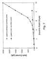
- Fig. 7 shows a plot of the dark current-voltage characteristics of a device with a unipolar buffer layer 22 made of Na-doped selenium film as shown on the left hand side of Fig. 2(b), and without such layer 22 as shown on the right hand side of Fig. 2(b).
- the biasing electrodes 32, 34 consisted, in this case, of Pd. It can be seen from the graph in Fig. 7 (where pA means picoamperes) that the two devices behave quite differently at high electric fields, with the device that has no unipolar buffer layer having a much greater dark current. This is attributed to field-assisted emission of holes from the Pd electrode 34 into the selenium film 18.
- the device with the unipolar conducting buffer layer 22 situated between the bias electrode 32 and the doped amorphous selenium film 18 has a much lower dark current at the same electric field. This is caused by the fact that any field-assisted injection of holes from the electrode material is abruptly stopped because these holes immediately get trapped in the Na-doped material. Once trapped, these holes actually lower the electric field at the electrode interface, which also tends to lower the hole injection rate.
- Fig. 8(a) shows the total current (dark current + X-ray current) as a function of time in the device without the unipolar buffer layer
- Fig. 8(b) shows the total current as a function of time in the device with the unipolar buffer layer.
- the dark current As measured during the interval between the X-ray pulses, increases in value during the presence of the X-rays, and takes more than 30 seconds to return to its previous value before the application of the X-rays.
- This enhanced dark current is due to hole injection from the top electrode to neutralize the X-ray generated negative space charge in the selenium layer.
- this dark current recovery time manifests itself in the form of an image lag inasmuch as an excess current still persists in that region of the detector long after the primary photocurrent has expired.
- Fig. 8(b) shows the results of the same test performed on the device with the unipolar buffer layer.
- the dark current remains stable during the application of the X-rays.
- the current drops abruptly to the device's dark current value that was there before the X-ray exposure began. This novel device does not exhibit the detrimental image lag that the previous device demonstrated.
Landscapes
- Physics & Mathematics (AREA)
- General Physics & Mathematics (AREA)
- Chemical & Material Sciences (AREA)
- Inorganic Chemistry (AREA)
- High Energy & Nuclear Physics (AREA)
- Life Sciences & Earth Sciences (AREA)
- Health & Medical Sciences (AREA)
- Molecular Biology (AREA)
- Spectroscopy & Molecular Physics (AREA)
- Measurement Of Radiation (AREA)
- Radiography Using Non-Light Waves (AREA)
- Photoreceptors In Electrophotography (AREA)
- Light Receiving Elements (AREA)
Applications Claiming Priority (2)
| Application Number | Priority Date | Filing Date | Title |
|---|---|---|---|
| CA002184667A CA2184667C (fr) | 1996-09-03 | 1996-09-03 | Plaque multicouche pour la radiographie et methode de fabrication de cette plaque |
| CA2184667 | 1996-09-03 |
Publications (2)
| Publication Number | Publication Date |
|---|---|
| EP0826983A1 true EP0826983A1 (fr) | 1998-03-04 |
| EP0826983B1 EP0826983B1 (fr) | 2006-06-14 |
Family
ID=4158838
Family Applications (1)
| Application Number | Title | Priority Date | Filing Date |
|---|---|---|---|
| EP97306672A Expired - Lifetime EP0826983B1 (fr) | 1996-09-03 | 1997-08-29 | Plaque multicouche pour imagerie à rayons X et procédé de fabrication |
Country Status (5)
| Country | Link |
|---|---|
| US (2) | US5880472A (fr) |
| EP (1) | EP0826983B1 (fr) |
| JP (1) | JP3761691B2 (fr) |
| CA (1) | CA2184667C (fr) |
| DE (1) | DE69736095T2 (fr) |
Cited By (15)
| Publication number | Priority date | Publication date | Assignee | Title |
|---|---|---|---|---|
| US6353229B1 (en) | 1998-07-08 | 2002-03-05 | Ftni Inc. | Direct conversion digital x-ray detector with inherent high voltage protection for static and dynamic imaging |
| US6546075B1 (en) | 1999-05-10 | 2003-04-08 | Epsirad Inc. | Energy sensitive detection systems |
| EP1357608A3 (fr) * | 2002-04-23 | 2003-12-03 | Shimadzu Corporation | Détecteur de rayons x |
| US7122803B2 (en) | 2005-02-16 | 2006-10-17 | Hologic, Inc. | Amorphous selenium flat panel x-ray imager for tomosynthesis and static imaging |
| US7233005B2 (en) | 2005-02-16 | 2007-06-19 | Hologic, Inc. | Amorphous selenium flat panel x-ray imager for tomosynthesis and static imaging |
| EP1780800A3 (fr) * | 2005-11-01 | 2007-07-11 | Fujifilm Corporation | Couche photoconductrice formant un panneau de prise d'images à rayonnement et panneau de prise d'images à rayonnement |
| EP1121719A4 (fr) * | 1999-07-26 | 2007-08-22 | Edge Medical Devices Ltd | Detecteur numerique pour imagerie radiologique |
| US7304308B2 (en) | 2005-02-16 | 2007-12-04 | Hologic, Inc. | Amorphous selenium flat panel x-ray imager for tomosynthesis and static imaging |
| US9786807B2 (en) | 2011-04-19 | 2017-10-10 | Empa | Thin-film photovoltaic device and fabrication method |
| US9837565B2 (en) | 2012-12-21 | 2017-12-05 | Flison Ag | Fabricating thin-film optoelectronic devices with added potassium |
| US10109761B2 (en) | 2014-05-23 | 2018-10-23 | Flisom Ag | Fabricating thin-film optoelectronic devices with modified surface |
| US10396218B2 (en) | 2014-09-18 | 2019-08-27 | Flisom Ag | Self-assembly pattering for fabricating thin-film devices |
| US10651324B2 (en) | 2016-02-11 | 2020-05-12 | Flisom Ag | Self-assembly patterning for fabricating thin-film devices |
| US10658532B2 (en) | 2016-02-11 | 2020-05-19 | Flisom Ag | Fabricating thin-film optoelectronic devices with added rubidium and/or cesium |
| US12041796B2 (en) | 2016-12-02 | 2024-07-16 | The Research Foundation For The State University Of New York | Fused multi-layer amorphous selenium sensor |
Families Citing this family (36)
| Publication number | Priority date | Publication date | Assignee | Title |
|---|---|---|---|---|
| CA2241779C (fr) * | 1998-06-26 | 2010-02-09 | Ftni Inc. | Detecteur d'image radiologique indirecte pour utilisation avec la radiologie |
| US6590224B2 (en) * | 2000-03-22 | 2003-07-08 | Fuji Photo Film Co., Ltd. | Image storage medium and method of manufacturing the same |
| JP4884593B2 (ja) * | 2000-03-22 | 2012-02-29 | 富士フイルム株式会社 | 画像記録媒体 |
| US6774385B2 (en) * | 2000-03-22 | 2004-08-10 | Fuji Photo Film Co., Ltd. | Image recording medium and method of manufacturing the same |
| JP2001264442A (ja) * | 2000-03-22 | 2001-09-26 | Fuji Photo Film Co Ltd | 画像記録媒体 |
| JP2002162474A (ja) * | 2000-11-27 | 2002-06-07 | Sharp Corp | 電磁波検出器およびその製造方法 |
| JP3678162B2 (ja) * | 2001-04-12 | 2005-08-03 | 株式会社島津製作所 | 放射線検出装置 |
| DE10136756C2 (de) * | 2001-07-27 | 2003-07-31 | Siemens Ag | Röntgendiagnostikeinrichtung mit einem flexiblen Festkörper-Röntgendetektor |
| CA2363663C (fr) * | 2001-11-22 | 2004-10-19 | Ftni Inc. | Detecteur a rayons x a ecran plat et a conversion directe avec suppression automatique des images fantomes |
| JP2003209232A (ja) * | 2002-01-15 | 2003-07-25 | Fuji Photo Film Co Ltd | 固体検出器 |
| US7122804B2 (en) * | 2002-02-15 | 2006-10-17 | Varian Medical Systems Technologies, Inc. | X-ray imaging device |
| US7282717B2 (en) * | 2003-02-27 | 2007-10-16 | Kabushiki Kaisha Toshiba | X-ray detector and X-ray examination apparatus using it |
| US6982424B2 (en) * | 2003-06-02 | 2006-01-03 | Ge Medical Systems Global Technology Company, Llc | X-ray and CT image detector |
| JP2005012049A (ja) * | 2003-06-20 | 2005-01-13 | Shimadzu Corp | 放射線検出器およびそれを備えた放射線撮像装置 |
| US7019304B2 (en) * | 2003-10-06 | 2006-03-28 | General Electric Company | Solid-state radiation imager with back-side irradiation |
| US7256402B1 (en) * | 2004-04-15 | 2007-08-14 | Denny Lee | Flat panel X-ray imager with a grid structure |
| EP1780802B1 (fr) * | 2005-11-01 | 2012-03-28 | Fujifilm Corporation | Détecteur d'images à rayons X à base de sélénium amorphe |
| US7723692B2 (en) | 2005-11-21 | 2010-05-25 | Fujifilm Corporation | Solid state radiation sensor and manufacturing method of the same |
| US7928401B2 (en) | 2006-06-14 | 2011-04-19 | Fujifilm Corporation | Radiation detecting system |
| JP5213005B2 (ja) * | 2006-12-18 | 2013-06-19 | 浜松ホトニクス株式会社 | 放射線検出器 |
| JP2008227036A (ja) | 2007-03-12 | 2008-09-25 | Fujifilm Corp | 放射線平面検出器 |
| EP1978563A3 (fr) * | 2007-03-23 | 2012-10-24 | FUJIFILM Corporation | Détecteur de radiations et procédé pour la fabrication d'une couche photoconductrice pour l'enregistrement de celles-ci |
| JP4907418B2 (ja) * | 2007-05-01 | 2012-03-28 | 富士フイルム株式会社 | 放射線画像検出器 |
| JP4739298B2 (ja) * | 2007-08-31 | 2011-08-03 | 富士フイルム株式会社 | 放射線画像検出器 |
| JP2008151795A (ja) * | 2007-12-25 | 2008-07-03 | Shimadzu Corp | X線検出器 |
| JP2009164215A (ja) * | 2007-12-28 | 2009-07-23 | Fujifilm Corp | 放射線画像検出装置および放射線画像検出器の製造方法 |
| JP5070130B2 (ja) * | 2008-05-26 | 2012-11-07 | 富士フイルム株式会社 | 放射線検出器 |
| US8258482B2 (en) * | 2008-05-28 | 2012-09-04 | Lawrence Livermore National Security, Llc | Energy resolution in semiconductor gamma radiation detectors using heterojunctions and methods of use and preparation thereof |
| JP5185003B2 (ja) * | 2008-07-25 | 2013-04-17 | 浜松ホトニクス株式会社 | 放射線検出器 |
| US8324582B2 (en) * | 2009-07-16 | 2012-12-04 | Lee Denny L | Direct conversion X-ray imaging device with strip electrodes |
| JP5583452B2 (ja) | 2010-03-31 | 2014-09-03 | 富士フイルム株式会社 | 電磁波情報検出装置および電磁波情報検出方法 |
| US9269838B2 (en) | 2011-12-09 | 2016-02-23 | Karim S. Karim | Radiation detector system and method of manufacture |
| KR20150027636A (ko) * | 2013-09-04 | 2015-03-12 | 삼성전자주식회사 | 잔류 전하 제거 방법, 이 방법을 이용한 엑스선 영상 촬영 방법 및 장치 |
| KR102729137B1 (ko) | 2015-07-14 | 2024-11-13 | 도스 스마트 이미징 | 디지털 이미징 시스템에서의 방사선 감지를 위한 장치 |
| US9698193B1 (en) | 2016-09-15 | 2017-07-04 | Ka Imaging Inc. | Multi-sensor pixel architecture for use in a digital imaging system |
| TWI652945B (zh) | 2017-12-20 | 2019-03-01 | 財團法人工業技術研究院 | 具有自動曝光偵測能力的輻射影像器以及其方法 |
Citations (6)
| Publication number | Priority date | Publication date | Assignee | Title |
|---|---|---|---|---|
| JPH04128848A (ja) * | 1990-09-20 | 1992-04-30 | Fuji Electric Co Ltd | 電子写真用感光体並びにその評価方法および製造方法 |
| US5198673A (en) * | 1992-01-23 | 1993-03-30 | General Electric Company | Radiation image detector with optical gain selenium photosensors |
| EP0573199A2 (fr) * | 1992-06-01 | 1993-12-08 | Xerox Corporation | Elément de reproduction d'images à rayons X, à base d'un alliage de sélénium déposé sur un substrat transparant |
| US5320927A (en) * | 1992-06-01 | 1994-06-14 | Xerox Corporation | Process for manufacturing an improved selenium alloy x-ray imaging member on transparent substrate |
| US5396072A (en) * | 1992-08-17 | 1995-03-07 | U. S. Philips Corporation | X-ray image detector |
| US5436101A (en) * | 1993-08-20 | 1995-07-25 | Xerox Corporation | Negative charging selenium photoreceptor |
Family Cites Families (15)
| Publication number | Priority date | Publication date | Assignee | Title |
|---|---|---|---|---|
| US3041166A (en) * | 1958-02-12 | 1962-06-26 | Xerox Corp | Xerographic plate and method |
| US3975635A (en) * | 1975-01-24 | 1976-08-17 | Xerox Corporation | Xeroradiographic plate |
| US4286033A (en) * | 1980-03-05 | 1981-08-25 | Xerox Corporation | Trapping layer overcoated inorganic photoresponsive device |
| US4338387A (en) * | 1981-03-02 | 1982-07-06 | Xerox Corporation | Overcoated photoreceptor containing inorganic electron trapping and hole trapping layers |
| JPS57197876A (en) * | 1981-05-29 | 1982-12-04 | Nippon Hoso Kyokai <Nhk> | Photoconductive film |
| DE3312264A1 (de) * | 1983-04-05 | 1984-10-11 | Siemens AG, 1000 Berlin und 8000 München | Vorrichtung zur aufnahme von roentgenbildern |
| US4770965A (en) * | 1986-12-23 | 1988-09-13 | Xerox Corporation | Selenium alloy imaging member |
| JPH0792610B2 (ja) * | 1987-06-10 | 1995-10-09 | 富士電機株式会社 | 電子写真用感光体 |
| JPS63316059A (ja) * | 1987-06-18 | 1988-12-23 | Fuji Electric Co Ltd | 電子写真用感光体 |
| JPH01316751A (ja) * | 1988-06-16 | 1989-12-21 | Fuji Electric Co Ltd | 電子写真用感光体 |
| JPH01316750A (ja) * | 1988-06-16 | 1989-12-21 | Fuji Electric Co Ltd | 電子写真用感光体 |
| US5023661A (en) * | 1989-04-10 | 1991-06-11 | Xerox Corporation | Precharging of the X-ray photoreceptor to eliminate the fatigue artifact |
| DE4011267C2 (de) * | 1989-04-12 | 1995-03-23 | Fuji Electric Co Ltd | Elektrofotografisches Aufzeichnungsmaterial |
| US5192634A (en) * | 1990-02-07 | 1993-03-09 | Dai Nippon Printing Co., Ltd. | A-selenium-tellurium photosensitive member and electrostatic information recording method |
| US5182624A (en) * | 1990-08-08 | 1993-01-26 | Minnesota Mining And Manufacturing Company | Solid state electromagnetic radiation detector fet array |
-
1996
- 1996-09-03 CA CA002184667A patent/CA2184667C/fr not_active Expired - Lifetime
-
1997
- 1997-03-28 US US08/827,512 patent/US5880472A/en not_active Expired - Lifetime
- 1997-08-29 DE DE69736095T patent/DE69736095T2/de not_active Expired - Lifetime
- 1997-08-29 EP EP97306672A patent/EP0826983B1/fr not_active Expired - Lifetime
- 1997-09-03 JP JP27790497A patent/JP3761691B2/ja not_active Expired - Lifetime
-
1998
- 1998-11-20 US US09/196,749 patent/US6171643B1/en not_active Expired - Lifetime
Patent Citations (6)
| Publication number | Priority date | Publication date | Assignee | Title |
|---|---|---|---|---|
| JPH04128848A (ja) * | 1990-09-20 | 1992-04-30 | Fuji Electric Co Ltd | 電子写真用感光体並びにその評価方法および製造方法 |
| US5198673A (en) * | 1992-01-23 | 1993-03-30 | General Electric Company | Radiation image detector with optical gain selenium photosensors |
| EP0573199A2 (fr) * | 1992-06-01 | 1993-12-08 | Xerox Corporation | Elément de reproduction d'images à rayons X, à base d'un alliage de sélénium déposé sur un substrat transparant |
| US5320927A (en) * | 1992-06-01 | 1994-06-14 | Xerox Corporation | Process for manufacturing an improved selenium alloy x-ray imaging member on transparent substrate |
| US5396072A (en) * | 1992-08-17 | 1995-03-07 | U. S. Philips Corporation | X-ray image detector |
| US5436101A (en) * | 1993-08-20 | 1995-07-25 | Xerox Corporation | Negative charging selenium photoreceptor |
Non-Patent Citations (1)
| Title |
|---|
| DATABASE WPI Section Ch Week 9225, Derwent World Patents Index; Class G08, AN 92-203175, XP002049821 * |
Cited By (21)
| Publication number | Priority date | Publication date | Assignee | Title |
|---|---|---|---|---|
| US6353229B1 (en) | 1998-07-08 | 2002-03-05 | Ftni Inc. | Direct conversion digital x-ray detector with inherent high voltage protection for static and dynamic imaging |
| US6546075B1 (en) | 1999-05-10 | 2003-04-08 | Epsirad Inc. | Energy sensitive detection systems |
| EP1121719A4 (fr) * | 1999-07-26 | 2007-08-22 | Edge Medical Devices Ltd | Detecteur numerique pour imagerie radiologique |
| EP1357608A3 (fr) * | 2002-04-23 | 2003-12-03 | Shimadzu Corporation | Détecteur de rayons x |
| US7554092B2 (en) | 2002-04-23 | 2009-06-30 | Shimadzu Corporation | X-ray detector |
| US7122803B2 (en) | 2005-02-16 | 2006-10-17 | Hologic, Inc. | Amorphous selenium flat panel x-ray imager for tomosynthesis and static imaging |
| US7233005B2 (en) | 2005-02-16 | 2007-06-19 | Hologic, Inc. | Amorphous selenium flat panel x-ray imager for tomosynthesis and static imaging |
| US7304308B2 (en) | 2005-02-16 | 2007-12-04 | Hologic, Inc. | Amorphous selenium flat panel x-ray imager for tomosynthesis and static imaging |
| EP1780800A3 (fr) * | 2005-11-01 | 2007-07-11 | Fujifilm Corporation | Couche photoconductrice formant un panneau de prise d'images à rayonnement et panneau de prise d'images à rayonnement |
| US9786807B2 (en) | 2011-04-19 | 2017-10-10 | Empa | Thin-film photovoltaic device and fabrication method |
| US9837565B2 (en) | 2012-12-21 | 2017-12-05 | Flison Ag | Fabricating thin-film optoelectronic devices with added potassium |
| US10153387B2 (en) | 2012-12-21 | 2018-12-11 | Flisom Ag | Fabricating thin-film optoelectronic devices with added potassium |
| US10109761B2 (en) | 2014-05-23 | 2018-10-23 | Flisom Ag | Fabricating thin-film optoelectronic devices with modified surface |
| US10431709B2 (en) | 2014-05-23 | 2019-10-01 | Flisom Ag | Fabricating thin-film optoelectronic devices with modified surface |
| US10672941B2 (en) | 2014-05-23 | 2020-06-02 | Flisom Ag | Fabricating thin-film optoelectronic devices with modified surface |
| US10396218B2 (en) | 2014-09-18 | 2019-08-27 | Flisom Ag | Self-assembly pattering for fabricating thin-film devices |
| US10651324B2 (en) | 2016-02-11 | 2020-05-12 | Flisom Ag | Self-assembly patterning for fabricating thin-film devices |
| US10658532B2 (en) | 2016-02-11 | 2020-05-19 | Flisom Ag | Fabricating thin-film optoelectronic devices with added rubidium and/or cesium |
| US10971640B2 (en) | 2016-02-11 | 2021-04-06 | Flisom Ag | Self-assembly patterning for fabricating thin-film devices |
| US11257966B2 (en) | 2016-02-11 | 2022-02-22 | Flisom Ag | Fabricating thin-film optoelectronic devices with added rubidium and/or cesium |
| US12041796B2 (en) | 2016-12-02 | 2024-07-16 | The Research Foundation For The State University Of New York | Fused multi-layer amorphous selenium sensor |
Also Published As
| Publication number | Publication date |
|---|---|
| CA2184667C (fr) | 2000-06-20 |
| US6171643B1 (en) | 2001-01-09 |
| DE69736095D1 (de) | 2006-07-27 |
| US5880472A (en) | 1999-03-09 |
| DE69736095T2 (de) | 2007-01-18 |
| EP0826983B1 (fr) | 2006-06-14 |
| JPH10104358A (ja) | 1998-04-24 |
| CA2184667A1 (fr) | 1998-03-04 |
| JP3761691B2 (ja) | 2006-03-29 |
Similar Documents
| Publication | Publication Date | Title |
|---|---|---|
| US5880472A (en) | Multilayer plate for x-ray imaging and method of producing same | |
| Kasap et al. | Review X-ray photoconductors and stabilized a-Se for direct conversion digital flat-panel X-ray image-detectors | |
| DE3316649C2 (fr) | ||
| US7667179B2 (en) | Radiation image detector | |
| US6552356B2 (en) | Image recording medium | |
| US8022451B2 (en) | Radiation detector | |
| US20080272320A1 (en) | Radiation image detector | |
| US6774385B2 (en) | Image recording medium and method of manufacturing the same | |
| EP1357608B1 (fr) | Détecteur de rayons x | |
| JP2009032975A (ja) | 放射線検出器 | |
| Kasap | Doped and Stabilized Amorphous Selenium Single and Multilayer Photoconductive Layers for X‐Ray Imaging Detector Applications | |
| JP5230791B2 (ja) | 放射線検出器 | |
| US7679158B2 (en) | Radiation image detector | |
| JP4884593B2 (ja) | 画像記録媒体 | |
| US7939814B2 (en) | Radiographic image detector | |
| JP2012154933A (ja) | 放射線検出器 | |
| JP2009162586A (ja) | 放射線検出器 | |
| Taniguchi et al. | A highly sensitive chalcogenide photoconductor in a near‐infrared wavelength region | |
| Lee et al. | Removal of trapped charge in selenium detectors | |
| US7247872B2 (en) | Image recording medium and method of producing the same | |
| Jung | X-ray-induced changes in optical properties of doped and undoped amorphous selenium | |
| JPH01269945A (ja) | 電子写真感光体 | |
| Vaezi-Nejad | Amorphous semiconductor photoreceptors and X-ray image sensors | |
| JP2011185942A (ja) | 画像記録媒体およびその製造方法 | |
| JPH0381774A (ja) | 感光性材料および電子写真用感光体 |
Legal Events
| Date | Code | Title | Description |
|---|---|---|---|
| PUAI | Public reference made under article 153(3) epc to a published international application that has entered the european phase |
Free format text: ORIGINAL CODE: 0009012 |
|
| AK | Designated contracting states |
Kind code of ref document: A1 Designated state(s): BE CH DE DK FR GB IT LI NL SE |
|
| 17P | Request for examination filed |
Effective date: 19980713 |
|
| RAP1 | Party data changed (applicant data changed or rights of an application transferred) |
Owner name: FTNI INC. |
|
| AKX | Designation fees paid |
Free format text: BE CH DE DK FR GB IT LI NL SE |
|
| RBV | Designated contracting states (corrected) |
Designated state(s): BE CH DE DK FR GB IT LI NL SE |
|
| 17Q | First examination report despatched |
Effective date: 20030902 |
|
| GRAP | Despatch of communication of intention to grant a patent |
Free format text: ORIGINAL CODE: EPIDOSNIGR1 |
|
| GRAS | Grant fee paid |
Free format text: ORIGINAL CODE: EPIDOSNIGR3 |
|
| GRAA | (expected) grant |
Free format text: ORIGINAL CODE: 0009210 |
|
| AK | Designated contracting states |
Kind code of ref document: B1 Designated state(s): BE CH DE DK FR GB IT LI NL SE |
|
| PG25 | Lapsed in a contracting state [announced via postgrant information from national office to epo] |
Ref country code: LI Free format text: LAPSE BECAUSE OF FAILURE TO SUBMIT A TRANSLATION OF THE DESCRIPTION OR TO PAY THE FEE WITHIN THE PRESCRIBED TIME-LIMIT Effective date: 20060614 Ref country code: IT Free format text: LAPSE BECAUSE OF FAILURE TO SUBMIT A TRANSLATION OF THE DESCRIPTION OR TO PAY THE FEE WITHIN THE PRESCRIBED TIME-LIMIT;WARNING: LAPSES OF ITALIAN PATENTS WITH EFFECTIVE DATE BEFORE 2007 MAY HAVE OCCURRED AT ANY TIME BEFORE 2007. THE CORRECT EFFECTIVE DATE MAY BE DIFFERENT FROM THE ONE RECORDED. Effective date: 20060614 Ref country code: CH Free format text: LAPSE BECAUSE OF FAILURE TO SUBMIT A TRANSLATION OF THE DESCRIPTION OR TO PAY THE FEE WITHIN THE PRESCRIBED TIME-LIMIT Effective date: 20060614 Ref country code: BE Free format text: LAPSE BECAUSE OF FAILURE TO SUBMIT A TRANSLATION OF THE DESCRIPTION OR TO PAY THE FEE WITHIN THE PRESCRIBED TIME-LIMIT Effective date: 20060614 |
|
| REG | Reference to a national code |
Ref country code: GB Ref legal event code: FG4D |
|
| REG | Reference to a national code |
Ref country code: CH Ref legal event code: EP |
|
| REF | Corresponds to: |
Ref document number: 69736095 Country of ref document: DE Date of ref document: 20060727 Kind code of ref document: P |
|
| PG25 | Lapsed in a contracting state [announced via postgrant information from national office to epo] |
Ref country code: SE Free format text: LAPSE BECAUSE OF FAILURE TO SUBMIT A TRANSLATION OF THE DESCRIPTION OR TO PAY THE FEE WITHIN THE PRESCRIBED TIME-LIMIT Effective date: 20060914 Ref country code: DK Free format text: LAPSE BECAUSE OF FAILURE TO SUBMIT A TRANSLATION OF THE DESCRIPTION OR TO PAY THE FEE WITHIN THE PRESCRIBED TIME-LIMIT Effective date: 20060914 |
|
| REG | Reference to a national code |
Ref country code: CH Ref legal event code: PL |
|
| ET | Fr: translation filed | ||
| PLBE | No opposition filed within time limit |
Free format text: ORIGINAL CODE: 0009261 |
|
| STAA | Information on the status of an ep patent application or granted ep patent |
Free format text: STATUS: NO OPPOSITION FILED WITHIN TIME LIMIT |
|
| 26N | No opposition filed |
Effective date: 20070315 |
|
| REG | Reference to a national code |
Ref country code: NL Ref legal event code: SD Effective date: 20130620 |
|
| REG | Reference to a national code |
Ref country code: DE Ref legal event code: R082 Ref document number: 69736095 Country of ref document: DE Representative=s name: MUELLER-BORE & PARTNER PATENTANWAELTE, EUROPEA, DE |
|
| REG | Reference to a national code |
Ref country code: FR Ref legal event code: TP Owner name: ANALOGIC CANADA CORPORATION, CA Effective date: 20130618 |
|
| REG | Reference to a national code |
Ref country code: GB Ref legal event code: 732E Free format text: REGISTERED BETWEEN 20130725 AND 20130731 |
|
| REG | Reference to a national code |
Ref country code: DE Ref legal event code: R082 Ref document number: 69736095 Country of ref document: DE Representative=s name: MUELLER-BORE & PARTNER PATENTANWAELTE PARTG MB, DE Effective date: 20130708 Ref country code: DE Ref legal event code: R082 Ref document number: 69736095 Country of ref document: DE Representative=s name: MUELLER-BORE & PARTNER PATENTANWAELTE, EUROPEA, DE Effective date: 20130708 Ref country code: DE Ref legal event code: R081 Ref document number: 69736095 Country of ref document: DE Owner name: ANALOGIC CANADA CORPORATION, SAINT-LAURENT, CA Free format text: FORMER OWNER: FTNI INC., MONTREAL, QUEBEC, CA Effective date: 20130708 Ref country code: DE Ref legal event code: R081 Ref document number: 69736095 Country of ref document: DE Owner name: ANALOGIC CANADA CORPORATION, CA Free format text: FORMER OWNER: FTNI INC., MONTREAL, CA Effective date: 20130708 |
|
| REG | Reference to a national code |
Ref country code: FR Ref legal event code: PLFP Year of fee payment: 20 |
|
| PGFP | Annual fee paid to national office [announced via postgrant information from national office to epo] |
Ref country code: NL Payment date: 20160819 Year of fee payment: 20 |
|
| PGFP | Annual fee paid to national office [announced via postgrant information from national office to epo] |
Ref country code: DE Payment date: 20160822 Year of fee payment: 20 Ref country code: GB Payment date: 20160819 Year of fee payment: 20 |
|
| PGFP | Annual fee paid to national office [announced via postgrant information from national office to epo] |
Ref country code: FR Payment date: 20160822 Year of fee payment: 20 |
|
| REG | Reference to a national code |
Ref country code: DE Ref legal event code: R071 Ref document number: 69736095 Country of ref document: DE |
|
| REG | Reference to a national code |
Ref country code: NL Ref legal event code: MK Effective date: 20170828 |
|
| REG | Reference to a national code |
Ref country code: GB Ref legal event code: PE20 Expiry date: 20170828 |
|
| PG25 | Lapsed in a contracting state [announced via postgrant information from national office to epo] |
Ref country code: GB Free format text: LAPSE BECAUSE OF EXPIRATION OF PROTECTION Effective date: 20170828 |