EP0827008A2 - Eine Flachbildschirmvorrichtung und deren Herstellungsverfahren - Google Patents
Eine Flachbildschirmvorrichtung und deren Herstellungsverfahren Download PDFInfo
- Publication number
- EP0827008A2 EP0827008A2 EP97306667A EP97306667A EP0827008A2 EP 0827008 A2 EP0827008 A2 EP 0827008A2 EP 97306667 A EP97306667 A EP 97306667A EP 97306667 A EP97306667 A EP 97306667A EP 0827008 A2 EP0827008 A2 EP 0827008A2
- Authority
- EP
- European Patent Office
- Prior art keywords
- substrate
- layer
- substrates
- liquid crystal
- crystal display
- Prior art date
- Legal status (The legal status is an assumption and is not a legal conclusion. Google has not performed a legal analysis and makes no representation as to the accuracy of the status listed.)
- Withdrawn
Links
- 238000004519 manufacturing process Methods 0.000 title claims abstract description 27
- 239000000758 substrate Substances 0.000 claims abstract description 129
- 125000006850 spacer group Chemical group 0.000 claims abstract description 63
- 238000013518 transcription Methods 0.000 claims abstract description 51
- 230000035897 transcription Effects 0.000 claims abstract description 51
- 239000004973 liquid crystal related substance Substances 0.000 claims abstract description 47
- 238000000034 method Methods 0.000 claims abstract description 43
- 230000004888 barrier function Effects 0.000 claims abstract description 24
- 230000031700 light absorption Effects 0.000 claims abstract description 19
- 239000000463 material Substances 0.000 claims description 15
- 229920000642 polymer Polymers 0.000 claims description 6
- 230000001678 irradiating effect Effects 0.000 claims description 5
- 230000001681 protective effect Effects 0.000 claims description 5
- 238000007789 sealing Methods 0.000 claims description 5
- 239000004372 Polyvinyl alcohol Substances 0.000 claims description 4
- 239000011521 glass Substances 0.000 claims description 4
- 229920000139 polyethylene terephthalate Polymers 0.000 claims description 4
- 229920002451 polyvinyl alcohol Polymers 0.000 claims description 4
- 235000019422 polyvinyl alcohol Nutrition 0.000 claims description 4
- 229920000036 polyvinylpyrrolidone Polymers 0.000 claims description 4
- 239000001267 polyvinylpyrrolidone Substances 0.000 claims description 4
- 235000013855 polyvinylpyrrolidone Nutrition 0.000 claims description 4
- 229910052724 xenon Inorganic materials 0.000 claims description 4
- FHNFHKCVQCLJFQ-UHFFFAOYSA-N xenon atom Chemical compound [Xe] FHNFHKCVQCLJFQ-UHFFFAOYSA-N 0.000 claims description 4
- 229910052736 halogen Inorganic materials 0.000 claims description 3
- 150000002367 halogens Chemical class 0.000 claims description 3
- 239000004642 Polyimide Substances 0.000 claims description 2
- PNEYBMLMFCGWSK-UHFFFAOYSA-N aluminium oxide Inorganic materials [O-2].[O-2].[O-2].[Al+3].[Al+3] PNEYBMLMFCGWSK-UHFFFAOYSA-N 0.000 claims description 2
- 239000003822 epoxy resin Substances 0.000 claims description 2
- 229920001568 phenolic resin Polymers 0.000 claims description 2
- 229920000515 polycarbonate Polymers 0.000 claims description 2
- 239000004417 polycarbonate Substances 0.000 claims description 2
- 229920000647 polyepoxide Polymers 0.000 claims description 2
- 229920001721 polyimide Polymers 0.000 claims description 2
- 239000000843 powder Substances 0.000 claims description 2
- 229920006337 unsaturated polyester resin Polymers 0.000 claims description 2
- SLGWESQGEUXWJQ-UHFFFAOYSA-N formaldehyde;phenol Chemical compound O=C.OC1=CC=CC=C1 SLGWESQGEUXWJQ-UHFFFAOYSA-N 0.000 claims 1
- 239000010408 film Substances 0.000 description 38
- 210000004027 cell Anatomy 0.000 description 15
- 239000000126 substance Substances 0.000 description 8
- 239000011159 matrix material Substances 0.000 description 7
- 239000003999 initiator Substances 0.000 description 4
- 230000003287 optical effect Effects 0.000 description 4
- 238000005979 thermal decomposition reaction Methods 0.000 description 4
- 238000002834 transmittance Methods 0.000 description 4
- 230000000903 blocking effect Effects 0.000 description 3
- 239000003086 colorant Substances 0.000 description 3
- 238000010586 diagram Methods 0.000 description 3
- 239000002360 explosive Substances 0.000 description 3
- 239000007789 gas Substances 0.000 description 3
- RAXXELZNTBOGNW-UHFFFAOYSA-N imidazole Natural products C1=CNC=N1 RAXXELZNTBOGNW-UHFFFAOYSA-N 0.000 description 3
- 239000000049 pigment Substances 0.000 description 3
- 239000000565 sealant Substances 0.000 description 3
- 239000000020 Nitrocellulose Substances 0.000 description 2
- -1 acryl Chemical group 0.000 description 2
- 230000003139 buffering effect Effects 0.000 description 2
- 238000006243 chemical reaction Methods 0.000 description 2
- 239000003795 chemical substances by application Substances 0.000 description 2
- 230000005684 electric field Effects 0.000 description 2
- 238000002347 injection Methods 0.000 description 2
- 239000007924 injection Substances 0.000 description 2
- 229920001220 nitrocellulos Polymers 0.000 description 2
- 239000004033 plastic Substances 0.000 description 2
- 229920003023 plastic Polymers 0.000 description 2
- 239000005020 polyethylene terephthalate Substances 0.000 description 2
- 238000007639 printing Methods 0.000 description 2
- 229920005989 resin Polymers 0.000 description 2
- 239000011347 resin Substances 0.000 description 2
- 238000005488 sandblasting Methods 0.000 description 2
- 239000010409 thin film Substances 0.000 description 2
- KXGFMDJXCMQABM-UHFFFAOYSA-N 2-methoxy-6-methylphenol Chemical compound [CH]OC1=CC=CC([CH])=C1O KXGFMDJXCMQABM-UHFFFAOYSA-N 0.000 description 1
- OMPJBNCRMGITSC-UHFFFAOYSA-N Benzoylperoxide Chemical compound C=1C=CC=CC=1C(=O)OOC(=O)C1=CC=CC=C1 OMPJBNCRMGITSC-UHFFFAOYSA-N 0.000 description 1
- BWGNESOTFCXPMA-UHFFFAOYSA-N Dihydrogen disulfide Chemical compound SS BWGNESOTFCXPMA-UHFFFAOYSA-N 0.000 description 1
- UFHFLCQGNIYNRP-UHFFFAOYSA-N Hydrogen Chemical compound [H][H] UFHFLCQGNIYNRP-UHFFFAOYSA-N 0.000 description 1
- 206010047571 Visual impairment Diseases 0.000 description 1
- 239000000853 adhesive Substances 0.000 description 1
- 230000001070 adhesive effect Effects 0.000 description 1
- RWCCWEUUXYIKHB-UHFFFAOYSA-N benzophenone Chemical compound C=1C=CC=CC=1C(=O)C1=CC=CC=C1 RWCCWEUUXYIKHB-UHFFFAOYSA-N 0.000 description 1
- 230000015572 biosynthetic process Effects 0.000 description 1
- 238000007796 conventional method Methods 0.000 description 1
- 210000002858 crystal cell Anatomy 0.000 description 1
- 230000001419 dependent effect Effects 0.000 description 1
- 238000000151 deposition Methods 0.000 description 1
- 238000007599 discharging Methods 0.000 description 1
- 239000000975 dye Substances 0.000 description 1
- 230000000694 effects Effects 0.000 description 1
- 239000005262 ferroelectric liquid crystals (FLCs) Substances 0.000 description 1
- 125000000524 functional group Chemical group 0.000 description 1
- QSHDDOUJBYECFT-UHFFFAOYSA-N mercury Chemical compound [Hg] QSHDDOUJBYECFT-UHFFFAOYSA-N 0.000 description 1
- 229910052753 mercury Inorganic materials 0.000 description 1
- 239000007769 metal material Substances 0.000 description 1
- 239000000203 mixture Substances 0.000 description 1
- IJGRMHOSHXDMSA-UHFFFAOYSA-N nitrogen Substances N#N IJGRMHOSHXDMSA-UHFFFAOYSA-N 0.000 description 1
- 229910052757 nitrogen Inorganic materials 0.000 description 1
- QJGQUHMNIGDVPM-UHFFFAOYSA-N nitrogen(.) Chemical compound [N] QJGQUHMNIGDVPM-UHFFFAOYSA-N 0.000 description 1
- 150000002978 peroxides Chemical class 0.000 description 1
- 238000000206 photolithography Methods 0.000 description 1
- 230000000704 physical effect Effects 0.000 description 1
- 229920006254 polymer film Polymers 0.000 description 1
- 239000002861 polymer material Substances 0.000 description 1
- 238000007650 screen-printing Methods 0.000 description 1
- 239000007787 solid Substances 0.000 description 1
- 239000012780 transparent material Substances 0.000 description 1
Images


Classifications
-
- G—PHYSICS
- G02—OPTICS
- G02F—OPTICAL DEVICES OR ARRANGEMENTS FOR THE CONTROL OF LIGHT BY MODIFICATION OF THE OPTICAL PROPERTIES OF THE MEDIA OF THE ELEMENTS INVOLVED THEREIN; NON-LINEAR OPTICS; FREQUENCY-CHANGING OF LIGHT; OPTICAL LOGIC ELEMENTS; OPTICAL ANALOGUE/DIGITAL CONVERTERS
- G02F1/00—Devices or arrangements for the control of the intensity, colour, phase, polarisation or direction of light arriving from an independent light source, e.g. switching, gating or modulating; Non-linear optics
- G02F1/01—Devices or arrangements for the control of the intensity, colour, phase, polarisation or direction of light arriving from an independent light source, e.g. switching, gating or modulating; Non-linear optics for the control of the intensity, phase, polarisation or colour
- G02F1/13—Devices or arrangements for the control of the intensity, colour, phase, polarisation or direction of light arriving from an independent light source, e.g. switching, gating or modulating; Non-linear optics for the control of the intensity, phase, polarisation or colour based on liquid crystals, e.g. single liquid crystal display cells
- G02F1/133—Constructional arrangements; Operation of liquid crystal cells; Circuit arrangements
- G02F1/1333—Constructional arrangements; Manufacturing methods
- G02F1/1339—Gaskets; Spacers; Sealing of cells
- G02F1/13394—Gaskets; Spacers; Sealing of cells spacers regularly patterned on the cell subtrate, e.g. walls, pillars
-
- H—ELECTRICITY
- H01—ELECTRIC ELEMENTS
- H01J—ELECTRIC DISCHARGE TUBES OR DISCHARGE LAMPS
- H01J9/00—Apparatus or processes specially adapted for the manufacture, installation, removal, maintenance of electric discharge tubes, discharge lamps, or parts thereof; Recovery of material from discharge tubes or lamps
- H01J9/24—Manufacture or joining of vessels, leading-in conductors or bases
- H01J9/241—Manufacture or joining of vessels, leading-in conductors or bases the vessel being for a flat panel display
- H01J9/242—Spacers between faceplate and backplate
-
- H—ELECTRICITY
- H01—ELECTRIC ELEMENTS
- H01J—ELECTRIC DISCHARGE TUBES OR DISCHARGE LAMPS
- H01J2211/00—Plasma display panels with alternate current induction of the discharge, e.g. AC-PDPs
- H01J2211/20—Constructional details
- H01J2211/34—Vessels, containers or parts thereof, e.g. substrates
- H01J2211/36—Spacers, barriers, ribs, partitions or the like
Definitions
- the present invention relates to a flat-panel display device, and more particularly, to a flat-panel display device and manufacturing method therefor, in which display characteristics are improved by uniformly maintaining a cell gap between upper and lower substrates.
- Cathode ray tube (CRT), and a flat-panel display device such as a liquid crystal display (LCD), a plasma display (PDP), electro-luminescent display (ELD), a field emitting device (FED) and a light emitting diode (LED) are currently used as picture display devices.
- LCD liquid crystal display
- PDP plasma display
- ELD electro-luminescent display
- FED field emitting device
- LED light emitting diode
- the CRT has excellent picture quality and brightness compared to other devices. However, the volume and weight of the CRT are great, so that it is difficult to be used for a large screen.
- An LCD is a display device using peculiar properties of liquid crystal.
- the liquid crystal is easy to handle and has a characteristic in which the alignment of the liquid crystals are changed according to the application of an external electrical field.
- the liquid crystal is widely used in ferroelectric liquid crystal devices (FLCD), twisted nematic LCD (TN-LCD), thin film transistor LCD (TFT-LCD) and plastic LCD.
- FIG. 1 is a sectional view showing the structure of a conventional LCD.
- ITO electrodes 12 and 12', alignment layers 13 and 13' are sequentially stacked on the transparent substrates 11 and 11', respectively, to form first and second substrates 10 and 10'.
- a spacer 14 is then scattered between the alignment layers 13 and 13' of the first and second substrates 10 and 10'.
- the first and second substrates 10 and 10' are sealed using sealant 16, resulting in a cell gap therebetween.
- liquid crystal is inserted into the cell gap to form a liquid crystal layer 15.
- An LCD having the above structure employs a characteristic that the alignment of the liquid crystals is changed by the application of an external voltage, and thus the light incident onto the liquid crystal layer is blocked or transmitted. That is, when an electrical field is formed in the liquid crystal layer by applying a voltage to the transparent electrode, the liquid crystals are aligned in a predetermined direction, and thus the light incident onto the liquid crystal layer is blocked or transmitted according to the alignment pattern of the liquid crystals.
- Such driving characteristics of the liquid crystals are largely influenced by the interval of the liquid crystal cell gap of the LCD.
- the physico-chemical reaction of the liquid crystals is determined according to the intensity of the applied voltage and the distance between the two electrodes, the physico-chemical reaction of the liquid crystals with respect to the voltage are changed and the transmittance ratio is not uniform, if the thickness of the liquid crystal layer is not uniform.
- circular or cylindrical spacers having larger diameters than the interval of the intended cell gap are scattered on the alignment layer of one of two substrates in which a transparent substrate, a transparent electrode and an alignment layer are sequentially deposited. Then, the other substrate is put on the substrate such that the alignment layers of two substrates face each other, and then a sealant as an adhesive material is applied at the borders of the two substrates. Therefore, the two substrates are sealed under pressure while applying heat or irradiating ultraviolet rays, forming a cell gap.
- the interval of the cell gap is controlled in the above manner, various problems occur.
- spacers are scattered irregularly, they may be partially agglomerated, resulting in a deviation in the interval of the cell gap. Further, the diameters of the spacers are uneven, so that it is difficult to evenly control the interval of the cell gap.
- the spacers are not fixed within the cell gap, they flow during the injection of the liquid crystal. Accordingly, the alignment layer may be damaged. Further, the electrodes may be damaged by the spacers when two substrates are sealed under pressure. Thus, the resultant LCD does not have good light blocking and transmittance characteristics.
- a spacer formation method using a photolithography technique has been suggested.
- a photosensitive material is deposited on the substrate to form a photosensitive layer, and then the photosensitive layer is exposed to the light and developed, resulting in spacers having the intended pattern.
- this method may cause damage to the alignment layer.
- a color LCD includes a first substrate including red, green and blue color filters as three principle colors of light, a second substrate including an active circuit portion with a thin film transistor, and a liquid crystal layer between two substrates.
- FIGS. 2 and 3 show the structure of the first substrate including a color filter layer in a color LCD.
- the process of forming the first substrate will now be described.
- a light shielding black matrix 22a (see FIG. 2) is formed on a transparent substrate 21.
- a photosensitive acryl resin including a dye with a spectroscopic property of red is deposited on the entire surface of the substrate 21, and then a red filter 23 is formed through baking, light-exposure and developing processes.
- a green filter 24 and a blue filter 25 are formed in the same manner as that of the red filter 23, thereby resulting in a color filter 20.
- the color filter may be in strips, dots or mosaic.
- FIG. 3 shows a substrate in which a black matrix 22b is formed after the step of forming a color filter layer 20.
- a protective film 26 may be formed of a transparent resin having strong surface hardness and excellent light transmittance in order to protect the black matrix 22a or 22b and the color filter layer 20 from external impact.
- a transparent electrode layer 27 for driving the liquid crystal is formed and then an alignment layer 28 is formed on the transparent electrode layer 27, completing the first substrate.
- three-wavelength lights emitted from the fluorescent lamp pass a filter layer for selectively transmitting only a predetermined wavelength light via a liquid crystal panel which is opened or closed by an electrical signal, so that a predetermined color (image) is achieved.
- the plasma display panel displays an image using a gas discharging phenomenon, which is excellent in display capacity, luminance and contrast. Also, there is little afterimage and a viewing angle is wide. Thus, the plasma display panel attracts attention as a next generation display device.
- the plasma display panel is manufactured by the following steps: first, two transparent substrates made of a transparent material such as glass are prepared. On the one of the transparent substrates, a transparent electrode in a stripe shape with a predetermined interval, a bus electrode in a stripe shape whose width is narrower than that of the transparent electrode, and a dielectric layer covering both the transparent electrode and the bus electrode are formed sequentially to complete a front substrate. On the other transparent substrate, an address electrode in a stripe shape which is orthogonal to that of the transparent electrode and a dielectric layer covering the address electrode are sequentially formed to complete a rear substrate. Also, barrier walls for maintaining a gap between two substrates to a predetermined level is formed between two dielectric layers of the front and rear substrates.
- the barrier walls are formed by repeating a screen printing process several times till the height of the barrier wall reaches a predetermined level.
- the height of the barrier wall obtained by this method is not even, so that the cell gap between the upper and lower substrates is not uniform. Thus, an electrical and optical blocking effect between adjacent cells is not achieved.
- a sand blasting method is used.
- the sand blasting method is however complicated, and the yield therefrom is very low.
- a laser transcription method was developed in the printing, typesetting and photographic fields thirty or more years ago.
- a transcription substance e.g., dye or pigment, included in a layer formed on a base film as a support is transcribed on a receiving film (glass or polymer film) according to an intended film pattern (US Patent Nos. 3,787,210 and 5,326,619).
- a mixture of the transcription material such as dye and pigment and nitrocellulose decomposed by light is deposited on a base film.
- the pigment or dye can be transcribed on a substrate by the explosive force of gas generated from the nitrocellulose through the thermal decomposition.
- the donor film has a structure in which a light absorption layer for providing transcription energy through a thermal decomposition reaction by absorbing light, and a transcription layer including a transcription substance are stacked on a film functioning as a support.
- the light absorption layer having a thickness of about 1,000 ⁇ absorbs light and transcribes the transcription substance using the explosive force of nitrogen or hydrogen gas generated during the thermal decomposition reaction.
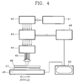
- FIG. 4 schematically showing a transcription apparatus used in a general laser transcription method.
- a high power laser beam is emitted from an energy source 41.
- the energy source emitting power at a rate of 0.1 ⁇ 4W a high power solid laser such as Nd/YAG, gas laser such as CO 2 and CO, or a diode-couple Nd/YAG can be used.
- the emitted laser beam is divided into a plurality of beams having the same intensity via a beam splitter 42. If the intensity of the beam is controlled by dividing the beam into a plurality of beams, a substance can be transcribed in a desired shape (U.S. Patent No. 4,796,038).
- the intensity of the plurality of divided laser beams is controlled by a modulator 43 according to an intended shape, and then the laser beam is irradiated on a donor film 46 on which the transcription substance is deposited, via a condensing optical system 44.
- a donor film 46 on which the transcription substance is deposited, via a condensing optical system 44.
- only the substance deposited on a light-receiving portion of the donor film is transcribed onto a substrate 47.
- the movement of a stage 48 is controlled together with a raster 49 for controlling the intensity of the bundle of the beam according to the shape of the desired pattern.
- the inventors of the present invention have conducted research into a method for forming a flat-panel display device of which a cell gap between upper and lower substrates are uniformly maintained using the above-described transcription method to thereby improve the display characteristics of the flat-panel display device.
- a liquid crystal display including first and second substrates in which a transparent substrate, a transparent electrode and an alignment layer are sequentially stacked, and a liquid crystal layer of which thickness is uniformly maintained by spacers formed between the alignment layers of the first and second substrates, wherein the height of each spacer and the interval between two adjacent spacers are constant.
- a method for manufacturing a liquid crystal display comprising the steps of: (a) forming first and second substrates in which transparent substrates, transparent electrodes and alignment layers are sequentially stacked, respectively; (b) placing a donor film including a base film, a light absorption layer and a transcription layer in a position depart from the alignment layer of the first substrate by a predetermined distance; (c) transcribing the spacer forming polymer of the transcription layer onto the first substrate by irradiating an energy source toward the base film of the donor film to form spacers, each spacer having equal height and the between two adjacent spacers being uniform; (d) stacking the second substrate on the first substrate on which spacers are transcribed so as to face the alignment layers of two substrates each other; and (e) sealing two substrates by hardening the spacers by providing light or heat to at least one of the first and second substrates to fix the spacers between the alignment layers of the first and second substrates.
- a plasma display panel including a first substrate in which a transparent substrate, an address electrode and a dielectric layer are stacked in sequence, a second substrate in which a transparent electrode, a bus electrode and a dielectric layer are stacked in sequence, and barrier walls formed between the first and second substrates to separate the first and second substrates by a predetermined distance, wherein each barrier wall has uniform height and width.
- a method for manufacturing a plasma display panel comprising the steps of: (a) forming a first substrate in which a transparent substrate, an address electrode and a dielectric layer are stacked in sequence; (b) forming a second substrate in which a transparent substrate, a transparent electrode, a bus electrode and a dielectric layer are stacked in sequence; (c) placing a donor film including a base film, a light absorption layer and a transcription layer in a position separated from the dielectric layer of the first substrate by a predetermined distance; (d) transcribing a barrier wall forming material of the transcription layer on the first substrate by irradiating a light source on the base film of the donor film to form barrier walls, each barrier wall having uniform height and width; (e) stacking the second substrate on the first substrate so as to face the dielectric layers of two substrates each other.
- FIG. 5 shows one embodiment of a liquid crystal display (LCD) according to one aspect of the present invention.
- reference numerals 51 and 51' represent first and second substrates
- reference numerals 52 and 52' represent transparent substrates
- reference numerals 53 and 53' represent transparent electrodes
- reference numerals 54 and 54' represent alignment layers
- reference numeral 55 represents a spacer formed by transcription method
- reference numeral 56 represents a liquid crystal layer, respectively.
- the spacers having a uniform height are formed at predetermined intervals.
- the LCD shown in FIG. 5 is formed by the following steps.
- two transparent substrates 52 and 52' are prepared, and the transparent electrodes 53 and 53' and the alignment layers 54 and 54' are sequentially stacked on each transparent substrate, to form the first and second substrates 51 and 51'.
- a donor film (not shown) including a base film, a light absorption layer and a transcription layer is positioned separated from the alignment layer 54 of the first substrate 51 by a predetermined interval.
- a light source is irradiated toward the base film of the donor film to transcribe a spacer forming material of the transcription layer onto the first substrate.
- the second substrate 51' is stacked on the first substrate 51 such that the alignment layers 54 and 54' of the first and second substrates 51 and 51' face each other.
- two substrates are sealed by applying light or heat to one of the first and second substrates, thereby completing a LCD.
- FIG. 6 is a diagram illustrating the step of transcribing the spacer forming material in detail.
- a transparent substrate 67, a transparent electrode 66, and an alignment layer 65 are sequentially stacked to form a first substrate.
- a light absorption layer 63 and a transcription layer 64 are sequentially deposited on a base film 62 to manufacture a donor film.
- a light source 61 is irradiated toward the base film 62.
- the irradiated energy activates the light absorption layer 63 via a laser transcription device 60 and the base film 62, so that transcription energy is emitted through the thermal decomposition reaction.
- the spacer forming material is transcribed onto the alignment layer.
- the donor film has a structure in which the base film, light absorption layer and transcription layer are stacked in sequence.
- the base film is formed of a material having light transmittance of 90% or more, such as polyethyleneterephthalate (PET) and polycarbonate.
- PET polyethyleneterephthalate
- polycarbonate a material having light transmittance of 90% or more
- the light absorption layer acts as a layer for converting the received light into transcription energy, and may include polymer or metal material.
- the transcription layer includes a spacer forming polymer as a main component, an initiator and a hardening agent.
- a spacer forming polymer as a main component, an initiator and a hardening agent.
- two substrate can be sealed by hardening the transcribed spacers by the following hardening step. That is, an extra substrate sealing step using a sealant is not necessary, so that the process is simplified.
- the polymer may be one selected from the group consisting of polyacryl, polyimide, polyvinylalcohol (PVA), polyvinylpyrrolidone (PVP), epoxy resin, phenol-formaldehyde resin and an unsaturated polyester resin.
- disulfide -S-S-
- peroxide -O-O-
- benzol peroxide may be used as an optical initiator
- benzophenon and imidazole may be used as a thermal initiator.
- the hardening agent may be anything which can be used in the field related with the present invention.
- a buffering layer may be further included between the light absorption layer and the transcription layer, which is for preventing the unevenness of the transcription layer, caused by the energy transmitted from the light absorption layer, and the partial transcription of the transcription layer together with the light absorption layer.
- UV/VIS light source such as a laser beam, xenon lamp or halogen lamp, or a thermal head may be used.
- the substrate may be sealed by hardening the spacers by providing light or heat energy from a proper light source.
- the light or heat energy source used for hardening the spacers may be the same as that used for the transcription, preferably, a high-pressure mercury lamp, a xenon lamp or a flash lamp.
- the height of each spacer is 0.5 ⁇ 10 ⁇ m, and the interval between adjacent two spacers is 10 ⁇ 1,000 ⁇ m.
- a color LCD may be manufactured by further forming a color filter layer consisting of color filters (red, green and blue filters) on one of two substrates. If required, a protective film may be further formed on the color filter layer.
- the spacers are formed in the liquid crystal layer corresponding to each portion between every adjacent two color filters, i.e., a portion in which black matrixes are to be formed, in a size so as to cover the portion between adjacent two color filters. Also, each spacer has an absorbency of 2 or more and a height of 0.5 ⁇ 10 ⁇ m.
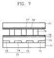
- FIG. 7 An LCD having the above structure is shown in FIG. 7.
- reference numerals 71 and 71' represent transparent substrates
- reference numeral 72 represents color filter layer
- reference numerals 73, 74 and 75 represent red, green and blue color filters
- reference numeral 76 represents protective film
- reference numerals 77 and 77' represent transparent electrodes
- reference numerals 78 and 78' represent alignment layers
- reference numerals 79 represent opaque spacers formed at positions where black matrixes are to be formed, respectively.
- the opaque spacers are formed in the positions where the black matrixes are to be formed such that the opaque spacers act as a black matrix as well as a spacer.
- the height of each opaque spacers formed by the above method is 0.5 ⁇ 10 ⁇ m which is greater than that (about 1,400 ⁇ ) of the conventional black matrix, so that the enhanced effect for preventing mixing of colors and improving the high-luminance characteristic can be achieved.
- a plasma display panel (PDP) of the present invention is manufactured by the following method:
- two transparent substrates are prepared.
- An address electrode and a dielectric layer are sequentially formed on the one of the transparent substrates, and a transparent electrode, a bus electrode and a dielectric layer are sequentially formed on the other transparent substrate, thereby resulting in first and second substrates.
- a donor film including a base film, a light absorption layer and a transcription layer is positioned separated from the dielectric layer of the first substrate by a predetermined distance.
- a light source is irradiated on the donor film to transcribe a barrier wall forming material onto the first substrate, and the second substrate is then stacked on the first substrate such that the dielectric layers of the first and second substrates face each other, thereby completing the PDP.
- the donor film has a structure in which the base film, light absorption layer and transcription layer are stacked in sequence.
- the base film and light absorption layer are the same as those described in the manufacturing method for the LCD, and the transcription layer may include a barrier wall forming material, such as alumina (Al 2 O 3 ) or glass powder.
- a barrier wall forming material such as alumina (Al 2 O 3 ) or glass powder.
- a buffering layer may be further included between the light absorption layer and the transcription layer.
- the light source used for the transcription is the same as that described in the manufacturing method for the LCD.
- the manufacturing method for the PDP may further include the step of forming multilayered barrier walls by repeating the transcription steps several times before the second substrate is stacked on the first substrate. As a result, barrier walls having the intended height can be obtained.
- the height and width of each barrier wall are 10 ⁇ several hundreds ⁇ m and 20 ⁇ 300 ⁇ m, respectively.
- the present invention provides the following advantages.
- the spacer forming material having a predetermined height is transcribed on an intended position, so that the spacers do not agglomerate as in the conventional spacer deposition method, resulting in a cell gap of even interval. Also, two substrates are sealed by hardening the transcribed spacers, so that an additional substrate sealing process is not required. Also, there is no damage to the electrode by the spacers, occurring during the conventional substrate sealing process under heat and pressure. Also, the spacer forming material is hardened by light (or heat) and then fixed between two substrates, so that the damage to the alignment layer during the injection of liquid crystals, caused by the flowing of spacers, can be prevented.
- the LCD and the manufacturing method therefor according to the present invention can be applied to manufacture FLCD, STN-LCD, TFT-LCD, TN-LCD and plastic LCD.
- each barrier wall having uniform height and width are formed, the electrical and optical blocking effect between adjacent cells, and resolution are remarkably enhanced, thereby improving display quality of an image.
- the manufacturing method for the PDP is simpler than the conventional method, and inferiority ratio is also low.
Landscapes
- Physics & Mathematics (AREA)
- Nonlinear Science (AREA)
- Mathematical Physics (AREA)
- Chemical & Material Sciences (AREA)
- Crystallography & Structural Chemistry (AREA)
- General Physics & Mathematics (AREA)
- Optics & Photonics (AREA)
- Engineering & Computer Science (AREA)
- Manufacturing & Machinery (AREA)
- Liquid Crystal (AREA)
- Devices For Indicating Variable Information By Combining Individual Elements (AREA)
Applications Claiming Priority (6)
| Application Number | Priority Date | Filing Date | Title |
|---|---|---|---|
| KR1019960037668A KR19980017847A (ko) | 1996-08-31 | 1996-08-31 | 컬러 액정표시소자 패널 및 그 제조방법 |
| KR9637668 | 1996-08-31 | ||
| KR1019960037667A KR19980017846A (ko) | 1996-08-31 | 1996-08-31 | 액정표시소자 패널 및 그 제조방법 |
| KR9637667 | 1996-08-31 | ||
| KR1019960041381A KR100406779B1 (ko) | 1996-09-20 | 1996-09-20 | 플라즈마 디스플레이 격벽 제조방법 |
| KR9641381 | 1996-09-20 |
Publications (2)
| Publication Number | Publication Date |
|---|---|
| EP0827008A2 true EP0827008A2 (de) | 1998-03-04 |
| EP0827008A3 EP0827008A3 (de) | 1998-11-18 |
Family
ID=27349387
Family Applications (1)
| Application Number | Title | Priority Date | Filing Date |
|---|---|---|---|
| EP97306667A Withdrawn EP0827008A3 (de) | 1996-08-31 | 1997-08-29 | Eine Flachbildschirmvorrichtung und deren Herstellungsverfahren |
Country Status (4)
| Country | Link |
|---|---|
| US (1) | US6124918A (de) |
| EP (1) | EP0827008A3 (de) |
| JP (2) | JPH1090688A (de) |
| CN (1) | CN1137405C (de) |
Cited By (1)
| Publication number | Priority date | Publication date | Assignee | Title |
|---|---|---|---|---|
| GB2332953A (en) * | 1998-01-06 | 1999-07-07 | Sharp Kk | Liquid crystal display element with spacers |
Families Citing this family (18)
| Publication number | Priority date | Publication date | Assignee | Title |
|---|---|---|---|---|
| JP2001005007A (ja) * | 1999-06-18 | 2001-01-12 | Hitachi Ltd | 液晶表示装置 |
| US6501526B1 (en) * | 1999-07-19 | 2002-12-31 | Institute For Advanced Engineering | Flat panel display apparatus having high aspect ratio spacers and method for manufacturing the same |
| US7394153B2 (en) * | 1999-12-17 | 2008-07-01 | Osram Opto Semiconductors Gmbh | Encapsulation of electronic devices |
| JP2003517182A (ja) * | 1999-12-17 | 2003-05-20 | オスラム オプト セミコンダクターズ ゲゼルシャフト ミット ベシュレンクテル ハフツング | 有機ledデバイスのカプセル封じ |
| US6762124B2 (en) | 2001-02-14 | 2004-07-13 | Avery Dennison Corporation | Method for patterning a multilayered conductor/substrate structure |
| KR100798308B1 (ko) * | 2001-05-11 | 2008-01-28 | 엘지.필립스 엘시디 주식회사 | 액정 표시소자의 스페이서 형성방법 |
| KR100483988B1 (ko) | 2001-11-29 | 2005-04-15 | 삼성에스디아이 주식회사 | 투명도전막의 투과도 변형방법 |
| JP4245990B2 (ja) * | 2003-06-23 | 2009-04-02 | シャープ株式会社 | 液晶表示装置、及びその製造方法 |
| JP2005209413A (ja) * | 2004-01-20 | 2005-08-04 | Sanyo Electric Co Ltd | 表示パネルの製造方法および表示パネル |
| CN101156107B (zh) * | 2005-02-03 | 2010-11-24 | 北卡罗来纳大学查珀尔希尔分校 | 用于液晶显示器的低表面能聚合物材料 |
| CN100410739C (zh) * | 2005-07-05 | 2008-08-13 | 中华映管股份有限公司 | 液晶显示面板与其修补方法 |
| US20080083484A1 (en) * | 2006-09-28 | 2008-04-10 | Graciela Beatriz Blanchet | Method to form a pattern of functional material on a substrate |
| KR100832241B1 (ko) * | 2006-11-03 | 2008-05-28 | 주식회사동양강철 | 알루미늄 합금 압출재를 이용한 디스플레이 패널용 보강프레임과 그 제조 방법 |
| KR101331058B1 (ko) | 2008-08-20 | 2013-11-20 | 라벤브릭 엘엘씨 | 열변색 필터를 제조하는 방법 |
| ES2616252T3 (es) | 2009-04-10 | 2017-06-12 | Ravenbrick, Llc | Filtro óptico conmutado térmicamente que incorpora una arquitectura de huésped-hospedador |
| US8947760B2 (en) | 2009-04-23 | 2015-02-03 | Ravenbrick Llc | Thermotropic optical shutter incorporating coatable polarizers |
| JP5862902B2 (ja) | 2010-06-01 | 2016-02-16 | レイブンブリック,エルエルシー | 多機能型構造用コンポーネント |
| JP5874683B2 (ja) | 2013-05-16 | 2016-03-02 | ソニー株式会社 | 実装基板の製造方法、および電子機器の製造方法 |
Family Cites Families (20)
| Publication number | Priority date | Publication date | Assignee | Title |
|---|---|---|---|---|
| US3787210A (en) * | 1971-09-30 | 1974-01-22 | Ncr | Laser recording technique using combustible blow-off |
| US4315668A (en) * | 1979-03-02 | 1982-02-16 | General Electric Company | Permeation barrier for display cells |
| JPS5642212A (en) * | 1979-09-17 | 1981-04-20 | Toshiba Corp | Liquid crystal display device |
| JPH0715536B2 (ja) * | 1983-01-28 | 1995-02-22 | キヤノン株式会社 | 表示パネル |
| US4796038A (en) * | 1985-07-24 | 1989-01-03 | Ateq Corporation | Laser pattern generation apparatus |
| US5171650A (en) * | 1990-10-04 | 1992-12-15 | Graphics Technology International, Inc. | Ablation-transfer imaging/recording |
| JPH03184022A (ja) * | 1989-12-13 | 1991-08-12 | Fujitsu Ltd | カラー液晶表示装置 |
| JPH049011A (ja) * | 1990-04-26 | 1992-01-13 | Matsushita Electric Ind Co Ltd | 液晶パネルの製法 |
| JP2981705B2 (ja) * | 1992-10-30 | 1999-11-22 | 株式会社住友金属エレクトロデバイス | プラズマディスプレイパネルの製造方法 |
| US5308737A (en) * | 1993-03-18 | 1994-05-03 | Minnesota Mining And Manufacturing Company | Laser propulsion transfer using black metal coated substrates |
| JP3394799B2 (ja) * | 1993-09-13 | 2003-04-07 | パイオニア株式会社 | プラズマディスプレイ装置 |
| US5593802A (en) * | 1993-10-07 | 1997-01-14 | Fuji Photo Film Co., Ltd. | Method of forming a spacer for use in a liquid crystal panel |
| JP3685821B2 (ja) * | 1993-10-07 | 2005-08-24 | 富士写真フイルム株式会社 | 液晶パネル用スペーサーの形成方法 |
| DE69427671T2 (de) * | 1993-10-19 | 2002-05-08 | Sharp Kk | Flüssigkristallanzeigevorrichtung und ihr Herstellungsverfahren |
| US5326619A (en) * | 1993-10-28 | 1994-07-05 | Minnesota Mining And Manufacturing Company | Thermal transfer donor element comprising a substrate having a microstructured surface |
| US5936694A (en) * | 1995-04-26 | 1999-08-10 | Canon Kabushiki Kaisha | Liquid crystal device and process for producing same |
| US5781258A (en) * | 1996-06-13 | 1998-07-14 | Rainbow Displays, Inc. | Assembling and sealing large, hermetic and semi-hermetic, h-tiled, flat-paneled displays |
| US5710097A (en) * | 1996-06-27 | 1998-01-20 | Minnesota Mining And Manufacturing Company | Process and materials for imagewise placement of uniform spacers in flat panel displays |
| JPH1090687A (ja) * | 1996-09-11 | 1998-04-10 | Machida Endscope Co Ltd | 液晶表示装置および液晶表示装置のスペーサー形成方法 |
| JP3750239B2 (ja) * | 1996-12-09 | 2006-03-01 | ソニー株式会社 | 画像表示装置 |
-
1997
- 1997-08-29 EP EP97306667A patent/EP0827008A3/de not_active Withdrawn
- 1997-08-29 CN CNB971206791A patent/CN1137405C/zh not_active Expired - Fee Related
- 1997-09-01 JP JP9235815A patent/JPH1090688A/ja active Pending
-
1999
- 1999-09-02 US US09/389,298 patent/US6124918A/en not_active Expired - Lifetime
-
2006
- 2006-02-01 JP JP2006025022A patent/JP4058077B2/ja not_active Expired - Fee Related
Cited By (2)
| Publication number | Priority date | Publication date | Assignee | Title |
|---|---|---|---|---|
| GB2332953A (en) * | 1998-01-06 | 1999-07-07 | Sharp Kk | Liquid crystal display element with spacers |
| GB2332953B (en) * | 1998-01-06 | 2002-07-17 | Sharp Kk | Liquid display element and manufacturing method thereof |
Also Published As
| Publication number | Publication date |
|---|---|
| MX9706601A (es) | 1998-05-31 |
| JP2006119679A (ja) | 2006-05-11 |
| EP0827008A3 (de) | 1998-11-18 |
| US6124918A (en) | 2000-09-26 |
| CN1137405C (zh) | 2004-02-04 |
| JPH1090688A (ja) | 1998-04-10 |
| CN1184953A (zh) | 1998-06-17 |
| JP4058077B2 (ja) | 2008-03-05 |
Similar Documents
| Publication | Publication Date | Title |
|---|---|---|
| US6124918A (en) | Method of manufacturing plasma display panel | |
| US5948577A (en) | Color filter substrate, liquid crystal display device using the same and method of manufacturing color filter substrate | |
| US20100277684A1 (en) | Display device and method for production thereof | |
| US20070058107A1 (en) | Photoluminescent liquid crystal display | |
| EP2645352A1 (de) | Anzeigevorrichtung und verfahren zu ihrer herstellung | |
| US7291975B2 (en) | Mask for organic electro-luminescence device and method of fabricating the same | |
| US11874437B2 (en) | Black structure and self-luminous image display device comprising same | |
| US7687781B2 (en) | External light shielding film and optical filter for display apparatus having the same | |
| KR100856015B1 (ko) | 액정 표시 장치 및 전자 기기 | |
| US20190250455A1 (en) | Display panel, manufacturing method thereof and display device | |
| US6225029B1 (en) | Plasma addressed liquid crystal display with organic-walled plasma channels | |
| KR100692872B1 (ko) | 마스크 및 그 제조방법과 그를 이용한 유기 전계 발광소자의 제조방법 | |
| KR101236515B1 (ko) | 액정 표시 장치용 컬러 필터 기판 및 그의 제조 방법 | |
| JP2004205974A (ja) | 2次元マトリクス素子、2次元マトリクス平面表示素子及びその駆動方法 | |
| JP6236793B2 (ja) | カラーフィルタ形成基板とカラーフィルタ形成基板の製造方法、および有機el表示装置 | |
| US7595585B2 (en) | Color conversion and optical enhancement layers for electroluminescent displays | |
| KR19980017847A (ko) | 컬러 액정표시소자 패널 및 그 제조방법 | |
| MXPA97006601A (en) | Flat panel display device and my elaboration method | |
| US6833895B2 (en) | Liquid crystal display device and fabrication method thereof | |
| KR19980057656A (ko) | 액정표시소자의 제조방법 | |
| KR100937822B1 (ko) | 이온 빔 조사 장치 및 그 방법 | |
| JPH07244213A (ja) | ブラックマトリクス基板の製造方法およびブラックマトリクス基板形成用樹脂 | |
| JP2003114319A (ja) | カラーフィルタの製造方法及びカラーフィルタ及び表示装置並びに電子機器 | |
| CN100380202C (zh) | 滤色片及电光学装置 | |
| JP3728803B2 (ja) | 水溶性感光性樹脂組成物 |
Legal Events
| Date | Code | Title | Description |
|---|---|---|---|
| PUAI | Public reference made under article 153(3) epc to a published international application that has entered the european phase |
Free format text: ORIGINAL CODE: 0009012 |
|
| AK | Designated contracting states |
Kind code of ref document: A2 Designated state(s): DE FR GB |
|
| AX | Request for extension of the european patent |
Free format text: AL;LT;LV;RO;SI |
|
| PUAL | Search report despatched |
Free format text: ORIGINAL CODE: 0009013 |
|
| AK | Designated contracting states |
Kind code of ref document: A3 Designated state(s): AT BE CH DE DK ES FI FR GB GR IE IT LI LU MC NL PT SE |
|
| AX | Request for extension of the european patent |
Free format text: AL;LT;LV;RO;SI |
|
| 17P | Request for examination filed |
Effective date: 19990217 |
|
| AKX | Designation fees paid |
Free format text: DE FR GB |
|
| STAA | Information on the status of an ep patent application or granted ep patent |
Free format text: STATUS: THE APPLICATION IS DEEMED TO BE WITHDRAWN |
|
| 18D | Application deemed to be withdrawn |
Effective date: 20040302 |